

EMI and layout fundamentals for switched mode circuits
.pdfvsg (t) |
|
|
|
|
EE core |
|
|
|
|
|
|
DTs |
Ts |
|
insulation |
|
|
secondary |
|||
|
|
|
|
|
||||||
|
|
|
|
|
primary |
|||||
|
|
|
Vpp |
t |
primary return |
|
|
|||
|
|
|
|
|
|
|
|
|
||
|
|
|
|
|
secondary return |
|
|
|
|
|
|
|
= n - 1 Vg + V |
Supplementary notes |
|
|
|
|
|
||
V |
|
|
on |
|
|
|
|
|
||
pp |
2 |
n |
|
|
|
|
|
|
||
iCM(t) |
|
|
|
|
|
n : 1 |
||||
|
|
|
|
|
|
|
|
|||
|
|
EMI andt Layout Fundamentals |
|
|
Cw |
|||||
|
|
|
|
|
||||||
|
|
|
for Switched-Mode Circuits |
|
|
|
Cw |
|||
|
|
|
|
|
|
|
|
|
|
|
|
|
|
|
R.W. Erickson LM |
iCM |
|
|
|
|
|
|
|
|
|
|
|
|
|
|
||
|
|
|
LM |
iCM |
1 |
|
|
– |
|
|
signal |
|
|
iDM |
|
V |
|
|
|||
|
|
|
: |
D1 |
|
|
||||
|
|
|
|
Vg |
1 |
|
+ |
|
|
|
|
|
|
|
+ |
|
|
|
|||
|
|
|
|
|
|
|
|
|
||
|
|
|
|
|
– |
|
|
|
|
+ |
|
|
|
|
i |
|
iCM |
|
i |
|
|
|
|
1 : 1 |
IDEAL |
|
|
|
|
|||
|
|
DM |
|
|
|
|
|
|||
|
|
|
|
|
|
CM |
vsg (t) |
|||
|
|
|
Q1 |
|
|
|
|
|||
return |
|
|
|
|
|
|
– |
|||
|
|
|
|
|
|
|
|
|
||
|
|
|
|
|
|
|
|
|
|
|
|
|
|
|
iCM |
iCM |
|
|
|
|
|
|
|
|
|
|
|
|
|
|
|
|
ECEN 5797 Power Electronics 1 |
|
Department of Electrical and Computer Engineering |
||||||||
|
|
University of Colorado at Boulder |
||||||||
|
|
|
|
|
|
|||||

EMI and Layout Fundamentals
for Switched-Mode Circuits
R.W. Erickson
•Introduction
•Idealizing assumptions made in beginning circuits
•Inductance of wires
•Coupling of signals via impedance of ground connections
•Parasitic capacitances
•The common mode
•Common-mode and differential-mode filters
ECEN 5797 Power Electronics 1 |
1 |
Department of Electrical and Computer Engineering |
|
University of Colorado at Boulder |
|||
|
|
||
|
|
|

Introduction
EMI (Electromagnetic Interference) is the unwanted coupling of signals from one circuit or system to another
Conducted EMI: unwanted coupling of signals via conduction through parasitic impedances, power and ground connections
Radiated EMI: unwanted coupling of signals via radio transmission
These effects usually arise from poor circuit layout and unmodeled parasitic impedances
Analog circuits rarely work correctly unless engineering effort is expended to solve EMI and layout problems
Sooner or later (or now!), the engineer needs to learn to deal with EMI
The ideal engineering approach:
–figure out what are the significant EMI sources
–figure out where the EMI is going
–engineer the circuit layout to mitigate EMI problems Build a layout that can be understood and analyzed
ECEN 5797 Power Electronics 1 |
2 |
Department of Electrical and Computer Engineering |
|
University of Colorado at Boulder |
|||
|
|
||
|
|
|

Assumptions made in Circuits 101 |
||||
1. Wires are perfect (equipotential) conductors |
||||
|
A |
Wire |
B |
|
|
|
|
|
VA = VB |
This assumption ignores |
|
|
||
• |
wire resistance |
|
|
|
• |
wire inductance |
|
|
|
• mutual inductance with other conductors |
||||
|
A |
|
B |
|
ECEN 5797 Power Electronics 1 |
|
3 |
Department of Electrical and Computer Engineering |
|
|
University of Colorado at Boulder |
|||
|
|
|
|
|
A related assumption:
1a. The space surrounding a wire is a perfect insulator (dielectric constant = 0)
This assumption ignores capacitance between conductors
A |
B |
||
|
|
|
|
|
|
|
|
ECEN 5797 Power Electronics 1 |
4 |
Department of Electrical and Computer Engineering |
|
University of Colorado at Boulder |
|||
|
|
||
|
|
|

2. The ground (reference) node is at zero potential
Formally, this is a definition. But there is an implicit assumption that all parts of the system can be connected via ideal conductors to a common ground node. In practice, it is often quite difficult to ensure that each stage of a system operates with the same zero potential reference.
|
|
|
|
|
|
|
|
|
|
|
|
|
|
|
|
|
|
|
|
|
|
|
|
|
|
|
|
|
|
|
|
Stage 1 |
|
Stage 2 |
|
Stage 3 |
|
|
|||||||||||||||||||||
|
|
|
|
|
|
|
|
|
|
|
|
|
|
|
|
|
|
|
|
|
|
|
|
|
|
|
|
|
|
|
|
|
|
|
|
|
|
|
|
|
|
|
|
|
|
|
|
|
|
|
|
|
|
|
|
|
|
|
|
|
|
|
|
|
|
|
|
|
|
|
|
|
|
|
|
|
|
|
|
|
|
|
|
|
|
|
|
|
|
|
|
|
|
|
|
|
|
|
|
|
|
|
|
|
|
|
|
|
|
|
|
|
|
|
|
|
|
|
|
|
|
|
|
|
|
|
|
|
|
|
|
|
|
|
|
|
|
|
|
|
|
|
|
|
|
|
|
|
|
Stage 1 |
Stage 2 |
Stage 3 |
ECEN 5797 Power Electronics 1 |
5 |
Department of Electrical and Computer Engineering |
|
University of Colorado at Boulder |
|||
|
|
||
|
|
|

We reinforce the problem by freely using the ground symbol
By use of this symbol, we avoid indicating how the actual wiring connection is made. In consequence, the possibility of conducted EMI via nonideal ground conductors is ignored
ECEN 5797 Power Electronics 1 |
6 |
Department of Electrical and Computer Engineering |
|
University of Colorado at Boulder |
|||
|
|
||
|
|
|
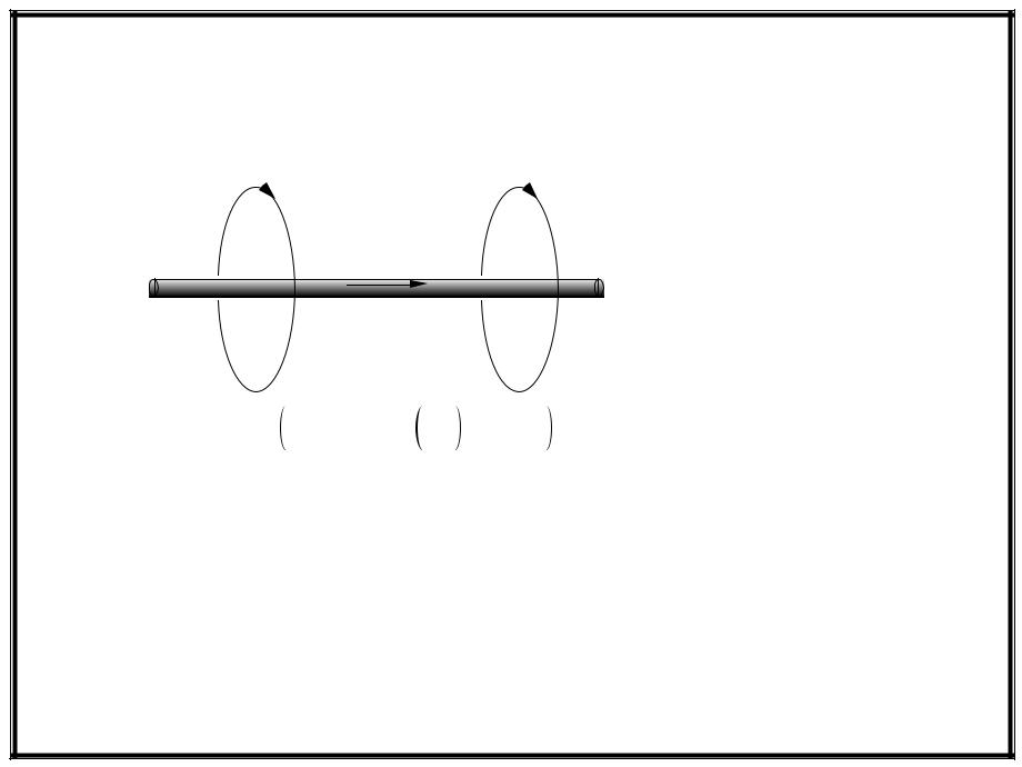
About inductance of wires
Single wire in space
B field
I
4l |
– 0.75 µH |
L = 0.00508 l 2.303 log10 d |
Terman, Radio Engineer's Handbook, p. 48ff, 1943
Self inductance L = λi
l |
= wire length |
d |
= wire diameter |
dimensions in inches
•Larger wire has lower inductance, because B-field must take longer path length around wire
•But how does the charge get back from end to beginning ? There is no closed loop, and so formula ignores area of loop
•Formula ignores effects of nearby conductors
ECEN 5797 Power Electronics 1 |
7 |
Department of Electrical and Computer Engineering |
|
University of Colorado at Boulder |
|||
|
|
||
|
|
|

A more realistic scenario:
current flows around a closed loop
|
B field |
I |
loop area A c |
single-turn air-core inductor
Simple-minded inductance formula:
L = |
µo AC |
µo = 4π 10-7 H/m |
|
lm |
lm = effective magnetic path length |
||
|
To reduce inductance: reduce loop cross-sectional area (by routing of wires), or increase path length (use larger wire).
ECEN 5797 Power Electronics 1 |
8 |
Department of Electrical and Computer Engineering |
|
University of Colorado at Boulder |
|||
|
|
||
|
|
|

Example: Buck converter
Use loop analysis |
|
Q1 |
|
+ |
i1(t) |
D1 |
i2(t) |
– |
|
||
|
|
|
i1(t) 
ILOAD
0
Q1 D1 conducts conducts
i2(t) 
ILOAD
ECEN 5797 Power Electronics 1
switched input current i1(t) contains large high frequency harmonics
—hence inductance of input loop is critical
inductance causes ringing, voltage spikes, switching loss, generation of B- and E- fields, radiated EMI
the second loop contains a filter inductor, and hence its current i2(t) is nearly dc
—hence additional inductance is not a significant problem in the second loop
9 |
Department of Electrical and Computer Engineering |
|
University of Colorado at Boulder |
||
|
||
|
|