

Physical layer specification.V1
.4.PDFIrDA Serial Infrared Physical Layer Specification, Version 1.4, February 6, 2001
2x Jitter
Figure 8. 4.0 Mbit/s Jitter Definitions
A.2.4. Eye Safety Standard
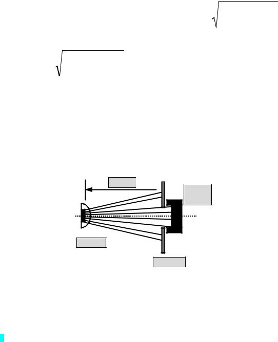
The apparent source size is a parameter used in determining the power or energy Accessible Emission Level Class limits and the measurement conditions of IEC 60825-1 and CENELEC EN60825-1.
The apparent source size is how large the source appears (how tightly the power or energy is concentrated). One method to determine apparent source size is to form an image of the source with a relay lens, as shown in Figure 9. By placing the emitter at a distance of twice the focal length of the lens, an image of size equal to the source will form at the same distance on the other side of the lens. The image can then be scanned with a small photodiode to determine the distribution of emitted light. Alternatively, a CCD camera system can be used; several of these systems on the market include software for analyzing the image.
scanner
emitter |
image |
|
|
|
relay lens |
Figure 9. Apparent Source Size Measurement
The apparent source size, s, is deemed to be the diameter of the smallest circular aperture containing approximately 63.2% of the incident light.
Measurements of source output power must be made at the correct distance, r, and with the correct aperture diameter, d. Under the amendment to IEC 60825-1 (and CENELEC EN60825-1) the measurement conditions for measuring output power, source to measurement aperture distance, r, and aperture diameter, d, are functions of apparent source size, s in mm or α (mrad). The eye safety standard used angles for defining source sizes. When using a fixed distance of 100mm, source size and apparent angular source size can be calculated simply by s (mm) = α (mrad)/10. The constants αmin and αmax are given with αmin = 1.5 mrad and αmax = 100mrad.
The measurement distance, r, measurement aperture diameter, d, are derived from apparent source size, s, as follows:
Aperture Diameter (d) |
Measurement Distance (r) |
|
|
33
IrDA Serial Infrared Physical Layer Specification, Version 1.4, February 6, 2001
Fixed 7.0 mm aperture in 14 mm to 100 mm |
r = (100mm)× |
α + 0.46mrad |
|
|||||
distance r |
|
|
|
|
||||
|
|
|
|
|
|
αmax |
||
|
|
|
|
|
|
|
||
|
|
|
|
|
|
if a < amin, r = 14 mm. If a ³ amax, r = 100 mm |
||
|
|
|
|
|
|
|
||
|
= ( |
)× |
|
αmax |
Variable 7 – 50 mm aperture d in 100 mm |
|||
|
|
distance |
|
|
||||
d |
7mm |
|
|
|
|
|
|
|
|
α + 0.46 mrad |
|
|
|
||||
|
|
|
|
|
|
|||
if a < amin, d = 50 mm. If a ³ amax, d = 7 mm |
|
|
|
|||||
|
|
|
|
|
|
|
|
|
|
|
|
|
Table 5. Measurement Parameters |
|
|
||
These relationships apply for s between 0.15 mm and 10 mm, which probably includes all IrDA compliant emitters.
A fixed aperture of 7.0 mm can be easier to implement, and then adjust the measurement distance according to the calculation. Whether the aperture is fixed at 7.0 mm or the distance is fixed at 100 mm, only light output power passing through the aperture is measured for comparison to the AEL Class limits.
distance 


 photodiode
emitter
aperture
Figure 10. IEC 60825-1 AEL Classification Power Measurement
Source output power can be derived from measured photocurrent resulting from light collected on a calibrated photodiode detector. Measured photocurrent in amps can be converted to detected power in watts, using the calibration factor in A/W (amps/watt).
For source wavelength l = 700-1050 nm, the AEL Class 1 limit is calculated as:
Parameters: IREDs 700 nm to 1050 nm, relevant time base, CW or averaged operation, thermal limits
|
|
|
|
|
|
|
|
|
|
Timebase [s] Conditions |
|
60825-1 Amendment 2 (Jan. 2001) |
|||||
|
Timebase = 100 s, |
7 x 10⁻⁴ |
C C W |
|
|
|||
|
a £ 1.5 mrad, t > T2 |
|
4 |
7 |
|
|
|
|
|
|
|
|
|
|
|
||
|
Timebase = 100 s, |
7 x 10⁻⁴ |
C C C T -0.25 |
W |
||||
|
a > 1.5 mrad, t > T2 |
|
4 |
6 |
7 |
2 |
|
|
|
|
|
|
|
|
|
||
|
Timebase = 100 s |
7 x 10⁻⁴ |
t0.75 |
C C C J |
|
|||
|
t £ T2 |
|
|
4 |
6 |
7 |
|
|
|
|
|
|
|
|
|
||
|
Constants |
|
|
|
|
|
|
|
|
C |
C = 100.02(λ-700) |
|
|
|
|||
|
4 |
4 |
|
|
|
|
|
|
34
|
IrDA Serial Infrared Physical Layer Specification, |
Version 1.4, February 6, 2001 |
||||||
|
|
|
|
|
|
|
|
|
C6 |
|
C6 = 1, α ≤ αmin |
|
|
|
|
||
C6 |
|
C6 |
= α/αmin, αmin < α < αmax |
|||||
C6 |
|
C6 |
= αmax/αmin = 66.7, α > αmax |
|||||
C7 |
|
C7 |
= 1 |
|
|
|
|
|
T |
|
|
é (α-α |
)ù |
||||
2 |
|
|
ê |
|
|
min |
|
ú |
|
|
|
|
98.5 |
|
|||
|
|
T = 10×10ë |
|
û s |
||||
|
|
|
|
|
||||
|
|
2 |
|
|
|
|
|
|
αmin |
|
αmin = 1.5 mrad |
|
|
|
|
||
|
|
αmax = 100 mrad |
|
|
|
|
||
Table 5a: Accessible emission limits for class 1 (and class 1M) laser products
The recent modification (effective January 2001) changes the minimum source angular subtense (1.5mrad as against 11mrad) and adds two break points for the exposure time t(T1 and T2). In case of IrDA transmission, the break point T2 is 10 s for α <1.5 mrad and 100s for α > 100 mrad.
For other cases, T2 is computed as given with the relation in the table above.
The relation between angular subtense α and apparent source size diameter s is given by α = 1000 x [2 x tan-1((s/2)/100 mm] (mrad)
s = apparent source size (mm)
The AEL Class 1 limit can be calculated by the formula given in the table above.
It is convenient to express both the AEL Class limit and the measured AEL of the system in terms of W/sr (watts/steradian). System source radiant intensity is often specified in mW/sr (milliwatts per steradian).
Apparent source angular subtense, α, is the 2-dimensional angle subtended by the source’s radiated light image at a distance of 100 mm. A 3-dimensional angle (solid angle) subtended by the source’s radiated light image can be expressed in units of steradians. A hemisphere (1/2 of a sphere) subtends a solid angle of 2π steradians. The solid angle, Ω, subtended by a cone of full angle, θ, is given by:
Ω = 2π (1 - cos( θ/2 ) )
Given the measurement distance, r, and the aperture diameter, d, the solid angle given by:
Ω = 2π (1 - cos( tan-1( d/2r )) )
The measured AEL and AEL Class limits can now be expressed in watts/steradian:
AEL (watts/steradian) = AEL (watts) / Ω (steradians)
Given the measurement distance, r, and the aperture diameter, d, the AEL is:
AEL (mW/sr) = AEL (mW)/ (2π (1 - cos( tan-1( d/2r )) ) )
Once the source radiant intensity in milliwatts/steradian has been determined, it can be compared with the AEL Class limits for classification. If the output does not exceed the Class 1 limit, the operation is Class 1. For more information, refer to IEC 60825-1 or CENELEC EN 60825-1 and their amendments.
A.3. Active Input Specifications
The following five specifications form a set which can be measured concurrently:
-Maximum Irradiance in Angular Range, mW/cm^2
-Minimum Irradiance in Angular Range, μW/cm^2
-Half-Angle, degrees
-Bit Error Ratio, (BER)
-Receiver Latency Allowance, ms
These measurements require an optical power source and means to measure angles and BERs. Since the optical power source must provide the specified characteristics of the Active Output, calibration and control of this source can use the same equipment as that required to measure the intensity and timing
35
IrDA Serial Infrared Physical Layer Specification, Version 1.4, February 6, 2001
characteristics. BER measurements require some method to determine errors in the received and decoded signal. The latency test requires exercise of the node's transmitter to condition the receiver.
Definitions of the reference point, etc., are the same as for the Active Output Interface optical power measurements except that the test head is now an optical power source with the in-band characteristics (Peak Wavelength, Rise and Fall Times, Pulse Duration, Signaling Rate and Jitter) of the Active Output Interface. The optical power source also must be able to provide the maximum power levels listed in the Active Output Specifications. It is expected that the minimum levels can be attained by appropriately spacing the optical source from the reference point.
Figure 11 illustrates the region over which the Optical High State is defined. The receiver is operated throughout this region and BER measurements are made to verify the maximum and minimum requirements. The ambient conditions of A.1 apply during BER tests; BER measurements can be done with worst case signal patterns. Unless otherwise known, the test signal pattern should include maximum length sequences of "1"s (no light) to test noise and ambient, and maximum length sequences of "0"s (light) to test for latency and other overload conditions.
The minimum allowable intensity value is indicated by “minimum” in Figure 11, since the actual specified value is dependent upon data rate.
Irradiance (or Incidance) (mW/cm2 )
|
|
|
|
|
|
(Vertical axis is not drawn to scale.) |
|||||||
Undefined Region |
|
|
|
|
|
|
|
|
500 |
|
|
||
|
|
Optical |
|
|
|
|
|
|
|
||||
|
|
|
|
|
|
|
|
|
|
|
|||
|
|
|
|
|
|
|
|
|
|
|
|
|
|
|
|
|
|
High |
|
|
|
|
|
|
Undefined Region |
||
|
|
|
|
State |
|
|
|
|
|
|
|||
|
|
|
|
|
|
|
|
|
|
|
|
|
|
|
|
|
|
|
|
|
|
|
|
|
minimum |
||
|
|
|
|
|
|
|
|
|
|
|
|||
|
|
|
|
|
|
|
|
|
|
|
|
|
|
|
|
|
|
|
|
|
|||||||
-30 |
-15 |
0 |
15 |
30 |
|
||||||||
|
|
|
|
Angle (Degrees) |
|
|
|
|
|||||
Figure 11. Optical High State Acceptable Range
Latency is tested at the Minimum Irradiance in Angular Range conditions. The receiver is conditioned by the exercise of its associated transmitter. For rates up to and including 1.152 Mbit/s, the conditioning signal should include maximum length sequences of "0"s (light) permitted for this equipment. For 4.0 Mbit/s 4PPM operation, various data strings should be used; the latency may be pattern dependent. The receiver is operated with the minimum irradiance levels and BER measurements are made after the specified latency period for this equipment to verify irradiance, half-angle, BER and latency requirements.
36
IrDA Serial Infrared Physical Layer Specification, Version 1.4, February 6, 2001
Appendix B. An Example of One End of a Link Implementation
Appendix B is Informative, not Normative {i.e., it does not contain requirements, but is for information only}. Specifications in Table 6 are derived from tables earlier in the document.
The link implementations in this appendix are examples only. All links must operate at 9.6 kbit/s. Specifications are used as constraints, but all other parameters' values are calculated for the purpose of providing a more complete example.
B.1. Definitions
UART - Universal Asynchronous Receiver/Transmitter: an electronic device/module that interfaces with a serial data channel.
B.2. Physical Representations
A block diagram of one end of an overall serial infrared link for data rates up to and including 115.2 kbit/s is shown in Figure 12a. Figure 12b shows on overall configuration for a link supporting the lower speeds as well as 0.576 Mbit/s, 1.152 Mbit/s and 4.0 Mbit/s.
|
|
|
|
|
|
|
|
|
|
|
|
|
|
|
|
|
|
|
|
|
|
|
|
|
|
|
|
|
|
|
|
|
|
|
|
|
|
|
|
|
|
|
|
|
|
|
|
|
|
|
|
|
|
|
|
|
|
|
|
|
|
|
IR Transmit |
|
|
|
|
|
|
|
Output |
|
|
IR Out |
|
|
||||
|
|
|
|
|
|
|
|
|
|
|
|
|
|
|
|
Driver |
|
|
|
|
||||||
|
|
|
|
|
|
|
|
|
|
|
Encoder |
|
|
|
|
|
|
|
|
|
|
Active |
|
|
||
|
|
|
|
|
|
|
|
|
|
|
|
|
|
|
|
|
|
& LED |
|
|
|
|
|
|||
|
|
16550 |
|
|
|
|
|
|
|
Encoder/ |
|
|
|
|
|
|
IR |
|
|
Output |
|
|
||||
|
|
|
|
|
|
|
|
|
|
|
|
|
|
|
|
|
Interface |
|
|
|||||||
[0] |
Compatible |
[1] |
|
|
Decoder |
[2] |
|
|
|
Transducer |
|
|
|
|
||||||||||||
|
|
|
|
|
[3] |
|
|
|
||||||||||||||||||
|
|
UART |
|
|
|
|
|
|
Module |
|
|
|
|
|
Module |
|
|
|
||||||||
|
|
|
|
|
|
|
|
|
|
|
|
|
|
|
||||||||||||
|
|
|
|
|
|
|
|
|
|
|
|
|
|
|
|
|
|
|||||||||
|
|
|
|
|
|
|
|
|
|
|
|
|
|
|
|
|
|
|
|
|
|
|
|
|
|
|
|
|
|
|
|
|
|
|
|
|
IR Receive |
|
|
|
|
|
|
|
Detector & |
|
|
IR In |
|
|
|||
|
|
|
|
|
|
|
|
|
|
|
Decoder |
|
|
|
|
|
|
|
Receiver |
|
|
|
Active |
|
|
|
|
|
|
|
|
|
|
|
|
|
|
|
|
|
|
|
|
|
|
|
|
|
|
|
Input |
|
|
|
|
|
|
|
|
|
|
|
|
|
|
|
|
|
|
|
|
|
|
|
|
|
Interface |
|
|
|
|
|
|
|
|
Figure 12a. Example of One End of Link |
|
|
|
||||||||||||||||||
|
|
|
|
|
|
|
|
|
|
|||||||||||||||||
|
|
For Signaling Rates Up to & Including 115.2 kb/s |
|
|
|
|
|
|||||||||||||||||||
|
|
|
|
|
|
|
|
|
|
|
|
|
|
|
|
|
|
|
|
|
|
|
|
Active |
|
|
|
|
|
|
|
|
|
|
|
|
|
Up To |
|
|
|
|
|
|
|
|
|
|
Output |
|
|
||
|
|
|
|
|
|
|
|
|
|
|
|
|
|
|
|
|
Output |
|
|
|
|
|||||
|
|
|
|
|
|
|
|
|
|
|
|
|
|
|
|
|
|
|
Interface |
|
|
|||||
|
|
|
|
|
|
|
|
|
|
|
|
|
|
|
|
|
|
|
|
|
||||||
|
|
|
|
|
|
|
|
|
|
|
115.2 kb/s |
|
|
|
|
|
|
Driver |
|
|
|
|
||||
|
|
|
|
|
|
|
|
|
|
|
|
|
|
|
|
|
|
|
|
|
||||||
|
|
|
|
|
|
|
|
|
|
|
|
|
|
|
|
|
|
|
|
|
||||||
|
|
|
|
|
|
|
|
|
|
|
|
|
|
|
|
|
|
|
|
|
|
|||||
|
|
|
|
|
|
|
|
|
|
|
|
|
|
|
|
|
|
|
||||||||
|
|
|
|
|
|
|
|
|
|
|
|
|
|
|
|
|
|
|
|
& LED |
|
|
IR Out |
|
|
|
|
|
|
|
|
|
|
|
|
|
|
|
|
|
|
|
|
|
|
|
|
|
|
|
|||
|
|
|
|
|
|
|
|
|
|
|
1.152 Mb/s |
|
|
|
|
|
|
|
|
|
|
|
|
|
||
|
|
|
|
|
|
|
|
|
|
|
|
|
|
|
|
|
IR |
|
|
|
|
|
||||
|
|
Comm. |
|
|
|
|
|
|
|
|
|
|
|
|
|
|
|
|
|
|
|
|||||
|
|
|
|
|
|
|
|
|
|
|
|
|
|
|
|
|
Transducer |
|
|
|
|
|
||||
|
|
|
|
|
|
|
|
|
|
|
|
|
|
|
|
|
|
|
|
|
|
|
|
|||
|
Controller |
|
|
|
|
|
|
|
|
|
|
|
|
|
|
|
Module |
|
|
|
|
|
||||
|
|
|
|
|
|
|
|
|
4.0 Mb/s |
|
|
|
|
|
|
|
|
|
|
|
||||||
|
|
|
|
|
|
|
|
|
|
|
|
|
|
|
|
|
|
|
|
|
|
|
|
|||
|
|
|
|
|
|
|
|
|
|
|
|
|
|
|
|
|
|
|
|
|
|
|
|
|||
|
|
|
|
|
|
|
|
|
|
|
|
|
|
|
Detector & |
|
|
IR In |
|
|
||||||
|
|
|
|
|
|
|
|
|
|
|
|
|
|
|
|
|
|
|
|
|
|
|
|
|||
|
|
|
|
|
|
|
|
|
|
|
|
|
|
|
|
|
|
|
|
|
|
|
|
|||
|
|
|
|
|
|
|
|
|
|
|
16.0 Mb/s |
|
|
|
|
|
|
Receiver |
|
|
Active |
|
|
|||
|
|
|
|
|
|
|
|
|
|
|
|
|
|
|
|
|
|
|
|
|
||||||
|
|
|
|
|
|
|
|
|
|
|
|
|
|
|
|
|
|
|
|
|
|
|
|
|
|
|
|
|
|
|
|
|
|
|
|
|
|
|
|
|
|
|
|
|
|
|
|
|
|
|
Input |
|
|
|
|
|
|
|
|
|
|
|
|
|
|
|
|
|
|
|
|
|
|
|
|
|
|
|
|
|
|
|
|
|
Figure 12 b. Example of One End of Link |
|
|
Interface |
|
|
|||||||||||||||||
|
|
|
|
|
For Signaling Rates Up to 16.0 Mb/s |
|
|
|
|
|
||||||||||||||||
37

IrDA Serial Infrared Physical Layer Specification, Version 1.4, February 6, 2001
B.3. Functionality & Electrical Waveforms - Data Rates Up to & Including 115.2 kbit/s
In Figure 12a, the signal to the left of the UART [0] will not be discussed. The signal between the UART and the Encoder/Decoder [1] is a bit stream of pulses in a frame comprised a Start Bit, 8 Data Bits, no Parity Bit and ending with a Stop Bit, as shown in Figure 13a.
The signal at [2], between the Encoder/Decoder Module and the IR Transducer Module is shown in Figure 13b. The electrical pulses between the IR Transmit Encoder and the Output Driver & LED are 3/16 of a bit period in duration (or, for the slower signaling rates, as short as 3/16 of the bit period for 115.2 kbit/s).
Note that the IR Transmit Encoder and the Output Driver and LED pulses begin at the center of the bit period. The electrical pulses between the Detector & Receiver and the IR Receive Decoder are nominally of the same duration as those between the IR Transmit Encoder and the Output Driver & LED, but may be longer in some implementations. Thus, the electrical signals at [2] are analogs of the optical signals at [3]; an example of a nominal waveform is shown in Figure 13b. A "0" is represented by a pulse and a "1" is represented by no pulse.
Start |
|
|
|
Bit |
|
|
|
0 |
1 |
0 |
1 |
UART Frame |
|
|
|
|
|
Data Bits |
|
|
|
|
Stop |
|
|
|
|
Bit |
|
|
|
|
|
|
|
0 |
0 |
1 |
1 |
0 |
1 |
Figure 13a. UART Frame
Start |
|
|
|
IR Frame |
|
|
|
|
|
|
|
Bit |
|
|
|
Data Bits |
|
0 |
1 |
0 |
1 |
0 |
0 |
|
|
|
Stop |
|
|
|
Bit |
1 |
1 |
0 |
1 |
Bit |
|
Figure 13b. IR Frame |
|
|
|
Pulse Width |
|
|
|
||||
Time |
|
|
|
|
3/16 Bit Time |
|
|
|
|
|
|
||
|
|
|
|
|
|
|
B.4. Receiver Data and Calculated Performance
Examples in this section are provided to show receiver implementations which are sufficient to meet the BER requirements called for in section 4 for minimum irradiance conditions. The highest signaling rate for each of the encoding formats is used due to the bandwidth and noise consequences. The sunlight ambient is also used for its noise impact.
Photodiode currents are calculated for the minimum signal and sunlight conditions. Different effective optically receptive areas are assumed for the standard and low power options. Noise and eye loss calculations are based on an assumed high input impedance preamplifier model with a single high frequency pole and a single low frequency pole forming a bandpass filter where the only noise sources are thermal noise due to the input impedance and shot noise due to sunlight generated photodiode current. The high frequency pole is set by the impedance and capacitance at the input of the preamplifier.
Preamplifier output rise time (Channel Response Time) is calculated combining preamplifier and Active Output characteristics. Eye loss due to minimum pulse width and channel response time limiting the amplitude to less than 100% of pulse magnitude is calculated. Eye loss due to jitter is not calculated and margin is provided for this and other considerations.
38
IrDA Serial Infrared Physical Layer Specification, Version 1.4, February 6, 2001
The three segments of Table 6 appear in specifications in section 4 of the main body of this document and are repeated here for convenient reference. Tables 7, 8 and 9 present examples of 115.2 kbit/s receiver implementations for standard, low power and mixed operation. Tables 10, 11 and 12 present similar examples for 1.152 Mbit/s implementations as do Tables 13, 14 and 15 for 4.0 Mbit/s operation. Tables 7 through 15 also repeat specifications for convenient reference.
TERMS:
Detector Responsivity (μA/(mW/cm2) is a photodiode characteristic combining sensitivity (A/W) and effective area.
Channel Response Time is the 10% to 90% rise time produced by the rms combination of the Active Output rise time and step response rise time of the preamplifier.
Receiver Noise Current is the thermal noise associated with the impedance at the input of the preamplifier and the associated bandwidth.
Sunlight Ambient Noise Current is the shot noise associated with the sunlight induced photodiode current and the associated bandwidth.
Receiver Noise Current is the rms combination of the receiver and sunlight ambient noise currents. Comparator Threshold is assumed to be at 50% of the minimum signal condition to yield optimum signal to noise ratios for both high and low states.
Specified Signal/Noise ratio for BER is the SNR calculated to achieve the required BER for a static signal level where the threshold is at 50% of the high state and noise is gaussian.
Receiver Margin is the ratio of the actual SNR to the Specified SNR for BER expressed in dB(optical).
Penalty: Eye Loss for Bandwidth Limits is the additional signal required for the minimum pulse width to reach 100% of the eye opening height expressed in dB(optical).
Margin for Edge Jitter, EMI, other is the signal margin above the Specified SNR for BER remaining after accounting for Eye Loss for Bandwidth Limits expressed in dB(optical).
39
IrDA Serial Infrared Physical Layer Specification, Version 1.4, February 6, 2001
|
LINK INTERFACE SPECIFICATIONS |
Data Rates |
Type |
Minimum |
Maximum |
||||
Signaling Rate |
|
|
|
|
All |
Both |
See Table 2 |
See Table 2 |
|
Link Distance Lower Limit, m |
|
|
All |
Both |
- |
0 |
|||
Minimum Link Distance Upper Limit, m |
|
See Table 1 |
Both |
See Table 1 |
- |
||||
Ambient Sunlight Irradiance**, μW/cm^2 |
|
|
Both |
- |
490 |
||||
Bit Error Ratio, BER |
|
|
|
|
All |
Both |
|
10^-8 |
|
|
ACTIVE OUTPUT SPECIFICATIONS |
|
|
|
|
|
|||
Peak Wavelength, Up, μm |
|
|
|
All |
Both |
0.85 |
0.90 |
||
Maximum Intensity In Angular Range, mW/sr |
|
All |
Std |
- |
500* |
||||
“ |
“ |
“ |
“ |
“ |
“ |
|
LowPwr |
- |
72* |
Minimum Intensity In Angular Range, mW/sr |
|
≤ 115.2 kbit/s |
Std |
40 |
- |
||||
“ |
“ |
“ |
“ |
“ |
“ |
≤ 115.2 kbit/s |
LowPwr |
3.6 |
- |
“ |
“ |
“ |
“ |
“ |
“ |
> 115.2 kbit/s |
Std |
100 |
- |
“ |
“ |
“ |
“ |
“ |
“ |
> 115.2 kbit/s |
LowPwr |
9 |
- |
Half-Angle, degrees |
|
|
|
|
All |
Both |
15 |
30 |
|
Rise Time tr, 10-90%, Fall Time Tf, 90-10% , ns |
≤ 115.2 kbit/s |
Both |
- |
600 |
|||||
Rise Time tr, 10-90%, Fall Time Tf, 90-10% , ns |
> 115.2 kbit/s |
Both |
- |
40 |
|||||
Rise Time tr, 10-90%, Fall Time Tf, 90-10% , ns |
16 Mbit/s |
Std |
- |
19 |
|||||
Pulse Duration |
|
|
|
|
All |
Both |
See Table 2 |
See Table 2 |
|
Edge Jitter, % of nominal pulse duration |
|
≤ 115.2 kbit/s |
Both |
- |
+/-6.5 |
||||
Edge Jitter Relative to Reference Clock, |
|
0.576 Mbit/s & |
Both |
- |
+/-2.9 |
||||
% of nominal bit duration |
|
|
1.152 Mbit/s |
|
|
|
|||
Edge Jitter, % of nominal chip duration |
|
4.0 Mbit/s |
Both |
- |
+/-4.0 |
||||
Edge Jitter, % of nominal chip duration |
|
16.0 Mbit/s |
Both |
- |
+/-4.0 |
||||
|
ACTIVE INPUT SPECIFICATIONS |
|
|
|
|
|
|||
Maximum Irradiance in Angular Range,mW/cm^2 |
All |
Both |
- |
500 |
|||||
Minimum Irradiance In Angular Range, μW/cm^2 |
≤ 115.2 kbit/s |
LowPwr |
9.0 |
- |
|||||
“ |
“ |
“ |
“ |
“ |
“ |
≤ 115.2 kbit/s |
Std |
4.0 |
- |
“ |
“ |
“ |
“ |
“ |
“ |
> 115.2 kbit/s |
LowPwr |
22.5 |
- |
“ |
“ |
“ |
“ |
“ |
“ |
> 115.2 kbit/s |
Std |
10.0 |
- |
Half-Angle, degrees |
|
|
|
|
All |
Both |
15 |
- |
|
Receiver Latency Allowance, ms |
|
|
All |
Std |
- |
10 |
|||
“ |
“ |
“ |
|
“ |
|
All |
LP |
- |
0.5 |
Receiver Latency Allowance, ms |
|
|
16.0 Mbit/s |
Both |
- |
0.1 |
|||
*For a given transmitter implementation, the IEC 60825-1 AEL Class 1 limit may be less than this. See section 2.4 above and Appendix A.
**Used for an example of ambient conditions. Allowance must be made for fluorescent and incandescent radiation as well as EMI.
Table 6. Serial Infrared Specifications for data rates up to 16.0 Mbit/s
40
IrDA Serial Infrared Physical Layer Specification, Version 1.4, February 6, 2001
B.4.1. 115.2 kbit/s Standard Implementation Example
(Standard transmitter to standard receiver for 115.2 kbit/s)
RECEIVER REQUIREMENTS & |
Minimum |
Maximum |
CALCULATED PERFORMANCE |
|
|
(Not Interface Specifications) |
|
|
Signal Pulse Rate, kbit/s |
114.2 |
116.2 |
Minimum Link Distance Upper Limit, m |
1.0 |
|
Detector Responsivity, μA/(mW/cm^2) |
44 |
|
|
|
|
Minimum Irradiance In Angular Range, μW/cm^2 |
4.0 |
|
Min. Eff. Receiver Signal Detected Current, nA |
175.8 |
- |
Sunlight In-Band Photocurrent, A |
2.15E-05 |
- |
|
|
|
Receiver Lower 3 dB Bandwidth Limit, MHz |
0.0015 |
|
Receiver Upper 3 dB Bandwidth Limit, MHz |
|
0.250 |
Receiver Input Noise Current, A |
3.95E-10 |
- |
Receiver Input Noise Current, A/(Hz)^0.5 |
7.93E-13 |
- |
Sunlight Ambient Noise Current, A |
1.64E-09 |
- |
Total Receiver Input rms Noise Current, A |
1.69E-09 |
- |
|
|
|
Comparator Threshold = 0.5(Signal), nA |
87.9 |
- |
Receiver Signal Detected/Input Noise Current |
104.2 |
- |
Specified Signal/Noise Ratio For BER |
11.2 |
- |
Receiver Margin (Min. S/N)/(Spec. S/N), dB |
9.68 |
- |
|
|
|
Single Bit Pulse Width, Tb, ns |
1410 |
- |
Channel Response Time, Tc, ns |
- |
1523 |
Penalty: Eye Loss for Bandwidth Limits, dB |
- |
0.93 |
|
|
|
Margin for Edge Jitter, EMI, other, dB |
8.8 |
- |
|
|
|
Table 7. Receiver Data and Calculated Performance for Standard Operation at 115.2 kbit/s
41
IrDA Serial Infrared Physical Layer Specification, Version 1.4, February 6, 2001
B.4.2. 115.2 kbit/s Low Power Option Implementation Example
(Low power transmitter to low power receiver for 115.2 kbit/s)
RECEIVER REQUIREMENTS & |
Minimum |
Maximum |
CALCULATED PERFORMANCE |
|
|
(Not Interface Specifications) |
|
|
Signal Pulse Rate, kbit/s |
114.2 |
116.2 |
Minimum Link Distance Upper Limit, m |
0.20 |
|
Detector Responsivity, μA/(mW/cm^2) |
17.2 |
|
|
|
|
Minimum Irradiance In Angular Range, μW/cm^2 |
9.0 |
|
Min. Eff. Receiver Signal Detected Current, nA |
154.5 |
- |
Sunlight In-Band Photocurrent, A |
8.41E-06 |
- |
|
|
|
Receiver Lower 3 dB Bandwidth Limit, MHz |
0.0015 |
|
Receiver Upper 3 dB Bandwidth Limit, MHz |
|
0.250 |
Receiver Input Noise Current, A |
2.44E-10 |
- |
Receiver Input Noise Current, A/(Hz)^0.5 |
4.89E-13 |
- |
Sunlight Ambient Noise Current, A |
1.02E-09 |
- |
Total Receiver Input rms Noise Current, A |
1.05E-09 |
- |
|
|
|
Comparator Threshold = 0.5(Signal), nA |
77.2 |
- |
Receiver Signal Detected/Input Noise Current |
146.6 |
- |
Specified Signal/Noise Ratio For BER |
11.2 |
- |
Receiver Margin (Min. S/N)/(Spec. S/N), dB |
11.17 |
- |
|
|
|
Single Bit Pulse Width, Tb, ns |
1410 |
- |
Channel Response Time, Tc, ns |
- |
1523 |
Penalty: Eye Loss for Bandwidth Limits, dB |
- |
0.93 |
|
|
|
Margin for Edge Jitter, EMI, other, dB |
10.2 |
- |
|
|
|
Table 8. Receiver Data and Calculated Performance for Low Power Operation at 115.2 kbit/s
42