


|
|
|
|
|
|
|
|
ATtiny28L/V |
|
|
|
|
|
|
|
|
|
|
Electrical Characteristics |
|
|
|||||
|
|
|
|
|||||
|
|
|
|
|||||
|
Absolute Maximum Ratings |
|
|
|
||||
|
|
|
*NOTICE: Stresses beyond those ratings listed under |
|||||
|
Operating Temperature............................. |
-40°C to +85/105°C |
||||||
|
|
|
|
|
|
|
“Absolute Maximum Ratings” may cause perma- |
|
|
Storage Temperature ..................................... |
-65°C to +150°C |
nent damage to the device. This is a stress rating |
|||||
|
|
|
|
|
|
|
only and functional operation of the device at |
|
|
Voltage on Any Pin except |
RESET |
|
|
these or other conditions beyond those indicated |
|||
|
with Respect to Ground ............................. |
-1.0V to VCC + 0.5V |
in the operational sections of this specification is |
|||||
|
Maximum Operating Voltage |
6.0V |
not implied. Exposure to absolute maximum rat- |
|||||
|
ing conditions for extended periods may affect |
|||||||
|
Voltage on |
|
with Respect to Ground -1.0V to +13.0V |
device reliability. |
||||
|
RESET |
|
|
|||||
|
DC Current per I/O Pin, except PA2 ........................... |
40.0 mA |
|
|
||||
|
DC Current PA2 .......................................................... |
60.0 mA |
|
|
||||
|
DC Current VCC and GND Pin................................. |
300.0 mA |
|
|
||||
|
|
|
|
|
|
|
|
|
DC Characteristics
TA = -40°C to 85°C, VCC = 1.8V to 5.5V (unless otherwise noted)
Symbol |
Parameter |
Condition |
|
|
|
Min |
Typ |
Max |
Units |
||
|
|
|
|
|
|
|
|
|
|
||
VIL |
Input Low Voltage |
(Except XTAL) |
|
|
|
-0.5 |
|
0.3 Vcc(1) |
V |
||
VIL1 |
Input Low Voltage |
XTAL |
|
|
|
-0.5 |
|
0.1 Vcc(1) |
V |
||
|
|
|
|
|
|
|
|
(2) |
|
|
|
VIH |
Input High Voltage |
(Except XTAL, RESET) |
|
VCC + 0.5 |
V |
||||||
0.6 VCC |
|
||||||||||
VIH1 |
Input High Voltage |
XTAL |
|
|
|
(2) |
|
VCC + 0.5 |
V |
||
|
|
|
0.7 VCC |
|
|||||||
VIH2 |
Input High Voltage |
RESET |
|
|
|
(2) |
|
VCC + 0.5 |
V |
||
|
|
|
0.85 VCC |
|
|||||||
VOL |
Output Low Voltage(3) |
IOL = 20 mA, VCC = 5V |
|
|
0.6 |
V |
|||||
|
Ports A, D |
IOL = 10 mA, VCC = 3V |
|
|
0.5 |
V |
|||||
VOL |
Output Low Voltage(3) |
IOL = 25 mA, VCC = 2.0V |
|
|
1.0 |
V |
|||||
|
Port A2 |
|
|
|
|
|
|
|
|
|
V |
V |
Output High Voltage(4) |
I |
OH |
= -3 mA, V |
|
= 5V |
4.3 |
|
|
V |
|
OH |
|
|
|
CC |
|
|
|
|
|||
|
Ports A, D |
IOH = -1.5 mA, VCC = 3V |
2.3 |
|
|
V |
|||||
IIL |
Input Leakage Current I/O Pin |
VCC = 5.5V, pin low |
|
|
8.0 |
µA |
|||||
|
|
(absolute value) |
|
|
|
|
|||||
|
|
|
|
|
|
|
|||||
IIL |
Input Leakage Current I/O Pin |
VCC = 5.5V, pin high |
|
|
8.0 |
µA |
|||||
|
|
(absolute value) |
|
|
|
|
|||||
|
|
|
|
|
|
|
|
|
|
|
|
RI/O |
I/O Pin Pull-up |
|
|
|
|
|
|
35.0 |
|
122.0 |
kΩ |
|
|
Active Mode, VCC = 3V, |
|
|
3.0 |
mA |
|||||
|
|
4 MHz |
|
|
|
|
|
|
|
||
|
|
|
|
|
|
|
|||||
|
|
Idle Mode VCC = 3V, 4 MHz |
|
1.0 |
1.2 |
mA |
|||||
ICC |
Power Supply Current |
Power-down(5)(6), VCC = 3V |
|
9.0 |
15.0 |
µA |
|||||
|
|
WDT enabled |
|
|
|
|
|
|
|
||
|
|
|
|
|
|
|
|||||
|
|
Power-down(5)(6), VCC = 3V |
|
<1.0 |
2.0 |
µA |
|||||
|
|
WDT disabled |
|
|
|
|
|
|
|
||
|
|
|
|
|
|
|
|
|
|
|
|
53
1062G–AVR–01/06

DC Characteristics (Continued)
TA = -40°C to 85°C, VCC = 1.8V to 5.5V (unless otherwise noted)
Symbol |
Parameter |
Condition |
Min |
Typ |
Max |
Units |
|
|
|
|
|
|
|
VACIO |
Analog Comparator Input |
VCC = 5V |
|
|
40.0 |
mV |
|
Offset Voltage |
VIN = VCC/2 |
|
|
|
|
IACLK |
Analog Comparator Input |
VCC = 5V |
-50.0 |
|
50.0 |
nA |
|
Leakage Current |
VIN = VCC/2 |
|
|
|
|
TACPD |
Analog Comparator |
VCC = 2.7V |
|
750.0 |
|
ns |
|
Propagation Delay |
VCC = 4.0V |
|
500.0 |
|
|
Notes: 1. “Max” means the highest value where the pin is guaranteed to be read as low.
2.“Min” means the lowest value where the pin is guaranteed to be read as high.
3.Although each I/O port can sink more than the test conditions (20 mA at VCC = 5V, 10 mA at VCC = 3V) under steady-state conditions (non-transient), the following must be observed:
1] The sum of all IOL, for all ports, should not exceed 300 mA.
2] The sum of all IOL, for port D0 - D7 and XTAL2 should not exceed 100 mA. If IOL exceeds the test condition, VOL may exceed the related specification. Pins are not guaranteed to sink current greater than the listed test conditions.
4.Although each I/O port can source more than the test conditions (3 mA at VCC = 5V, 1.5 mA at VCC = 3V) under steady-state conditions (non-transient), the following must be observed:
1] The sum of all IOH, for all ports, should not exceed 300 mA.
2] The sum of all IOH, for port D0 - D7 and XTAL2 should not exceed 100 mA. If IOH exceeds the test condition, VOH may exceed the related specification.
Pins are not guaranteed to source current greater than the listed test conditions.
5.Minimum VCC for power-down is 1.5V.
6.When entering Power-down, PORTA2 bit in PORTA register should be set.
54 ATtiny28L/V
1062G–AVR–01/06

ATtiny28L/V
External Clock Drive Waveforms
Figure 40. External Clock
VIH1
VIL1
External Clock Drive
|
|
|
|
VCC = 1.8V to 2.7V |
VCC = 2.7V to 4.0V |
VCC = 4.0V to 5.5V |
|
||||||
Symbol |
Parameter |
|
Min |
|
Max |
Min |
Max |
Min |
|
Max |
Units |
||
|
|
|
|
|
|
|
|
|
|
|
|
|
|
1/tCLCL |
Oscillator Frequency |
|
0.0 |
|
1.2 |
0.0 |
|
4.0 |
0.0 |
|
4.0 |
MHz |
|
tCLCL |
Clock Period |
|
833.0 |
|
|
250.0 |
|
250.0 |
|
|
ns |
||
tCHCX |
High Time |
|
333.0 |
|
|
100.0 |
|
100.0 |
|
|
ns |
||
tCLCX |
Low Time |
|
333.0 |
|
|
100.0 |
|
100.0 |
|
|
ns |
||
tCLCH |
Rise Time |
|
|
|
1.6 |
|
|
1.6 |
|
|
0.5 |
µs |
|
tCHCL |
Fall Time |
|
|
|
1.6 |
|
|
1.6 |
|
|
0.5 |
µs |
|
|
: |
|
|
|
|
|
|
|
|
|
|
|
|
Table 25. External RC Oscillator, Typical Frequencies |
|
|
|
|
|
|
|
||||||
|
|
|
|
|
|
|
|
|
|
|
|||
|
R [kΩ] |
|
|
|
C [pF] |
|
|
|
f |
|
|
||
|
|
|
|
|
|
|
|
|
|
|
|
||
|
100.0 |
|
|
|
70.0 |
|
|
|
100.0 kHz |
|
|
||
|
|
|
|
|
|
|
|
|
|
|
|
||
|
31.5 |
|
|
|
20.0 |
|
|
|
1.0 MHz |
|
|
||
|
|
|
|
|
|
|
|
|
|
|
|
||
|
6.5 |
|
|
|
20.0 |
|
|
|
4.0 MHz |
|
|
||
|
|
|
|
|
|
|
|||||||
|
Note: |
R should be in the range 3 - 100 kΩ, and C should be at least 20 pF. |
|
|
|||||||||
55
1062G–AVR–01/06

Typical
Characteristics
The following charts show typical behavior. These figures are not tested during manufacturing. All current consumption measurements are performed with all I/O pins configured as inputs and with internal pull-ups enabled. A sine wave generator with rail- to-rail output is used as clock source.
The power consumption in Power-down mode is independent of clock selection.
The current consumption is a function of several factors, such as: operating voltage, operating frequency, loading of I/O pins, switching rate of I/O pins, code executed and ambient temperature. The dominating factors are operating voltage and frequency. The current drawn from capacitive loaded pins may be estimated (for one pin) as CL • VCC • f, where CL = Load Capacitance, VCC = Operating Voltage and f = Average Switching Frequency of I/O pin.
The parts are characterized at frequencies and voltages higher than test limits. Parts are not guaranteed to function properly at frequencies and voltages higher than the ordering code indicates.
The difference between current consumption in Power-down mode with Watchdog Timer enabled and Power-down mode with Watchdog Timer disabled represents the differential current drawn by the Watchdog Timer.
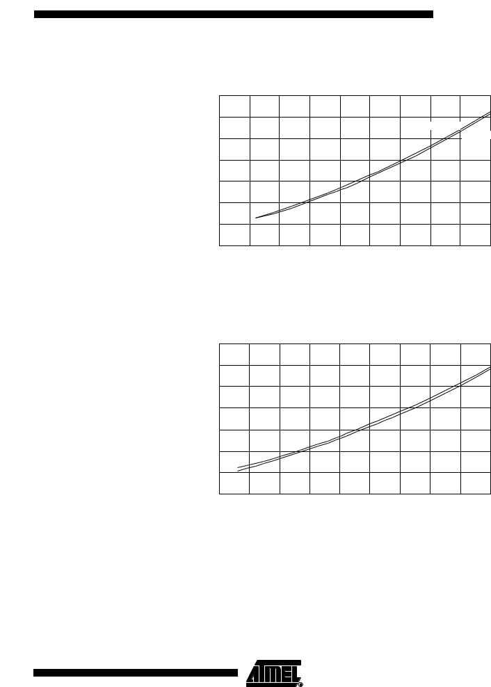
Figure 41. Active Supply Current vs. Frequency
ACTIVE SUPPLY CURRENT vs. FREQUENCY
|
|
|
|
|
|
|
|
TA = 25˚C |
|
|
|
|
|
|
|
|
|
18 |
|
|
|
|
|
|
|
|
|
|
|
|
|
|
|
|
16 |
|
|
|
|
|
|
|
|
|
|
|
|
|
VCC = 6.0V |
|
|
14 |
|
|
|
|
|
|
|
|
|
|
|
|
|
VCC = 5.5V |
|
|
12 |
|
|
|
|
|
|
|
|
|
|
|
|
|
VCC = 5.0V |
|
(mA) |
10 |
|
|
|
|
|
|
|
|
|
|
|
|
VCC = 4.5V |
|
|
|
|
|
|
|
|
|
|
|
|
|
|
|
|
|||
CC |
8 |
|
|
|
|
|
|
|
|
|
|
|
|
|
|
|
I |
|
|
|
|
|
|
|
|
|
|
|
|
VCC = 4.0V |
|
||
|
|
|
|
|
|
|
|
|
|
|
|
|
|
|
||
|
6 |
|
|
|
|
|
|
|
|
|
|
|
VCC = 3.6V |
|
|
|
|
4 |
|
|
|
|
|
|
|
|
|
VCC = 3.3V |
|
|
|
|
|
|
|
|
|
|
|
|
|
|
|
VCC = 3.0V |
|
|
|
|
||
|
|
|
|
|
|
|
|
|
|
|
|
|
|
|
||
|
2 |
|
|
|
|
|
|
|
|
VCC = 2.7V |
|
|
|
|
|
|
|
|
|
|
|
VCC = 2.1V |
|
|
VCC = 2.4V |
|
|
|
|
|
|
||
|
0 |
|
|
|
|
|
|
|
|
|
|
|
|
|
||
|
VCC = 1.8V |
|
|
|
|
|
|
|
|
|
|
|
|
|
|
|
|
|
|
|
|
|
|
|
|
|
|
|
|
|
|
|
|
|
0 |
1 |
2 |
3 |
4 |
5 |
6 |
7 |
8 |
9 |
10 |
11 |
12 |
13 |
14 |
15 |
Frequency (MHz)
56 ATtiny28L/V
1062G–AVR–01/06

ATtiny28L/V
Figure 42. Active Supply Current vs. VCC
ACTIVE SUPPLY CURRENT vs. VCC
ICC (mA)
FREQUENCY = 4 MHz
8
7
TA = 25˚C
6
TA = 85˚C
5
4
3
2
1
0
1.5 |
2 |
2.5 |
3 |
3.5 |
4 |
4.5 |
5 |
5.5 |
6 |
|
|
|
|
VCC (V) |
|
|
|
|
|
Figure 43. Active Supply Current vs. VCC, Device Clocked by Internal Oscillator
ACTIVE SUPPLY CURRENT vs. Vcc
DEVICE CLOCKED BY 1.2MHz INTERNAL RC OSCILLATOR
|
6 |
|
|
|
|
|
|
|
|
|
|
5 |
|
|
|
|
|
|
|
|
|
|
|
|
|
|
|
|
|
TA = 25˚C |
|
|
|
4 |
|
|
|
|
|
|
|
|
|
|
|
|
|
|
|
|
|
|
TA = 85˚C |
|
(mA) |
3 |
|
|
|
|
|
|
|
|
|
|
|
|
|
|
|
|
|
|
|
|
cc |
|
|
|
|
|
|
|
|
|
|
I |
|
|
|
|
|
|
|
|
|
|
|
2 |
|
|
|
|
|
|
|
|
|
|
1 |
|
|
|
|
|
|
|
|
|
|
0 |
|
|
|
|
|
|
|
|
|
|
1.5 |
2 |
2.5 |
3 |
3.5 |
4 |
4.5 |
5 |
5.5 |
6 |
Vcc(V)
57
1062G–AVR–01/06

Figure 44. Active Supply Current vs. VCC, Device Clocked by External 32 kHz Crystal
ACTIVE SUPPLY CURRENT vs. VCC
DEVICE CLOCKED BY 32 kHz CRYSTAL
|
4 |
|
|
|
|
|
|
|
|
|
|
3.5 |
|
|
|
|
|
|
|
|
|
|
|
|
|
|
|
|
|
TA = 25˚C |
|
|
|
3 |
|
|
|
|
|
|
|
|
|
|
|
|
|
|
|
|
|
|
TA = 85˚C |
|
|
2.5 |
|
|
|
|
|
|
|
|
|
(mA) |
2 |
|
|
|
|
|
|
|
|
|
CC |
|
|
|
|
|
|
|
|
|
|
|
|
|
|
|
|
|
|
|
|
|
I |
|
|
|
|
|
|
|
|
|
|
|
1.5 |
|
|
|
|
|
|
|
|
|
|
1 |
|
|
|
|
|
|
|
|
|
|
0.5 |
|
|
|
|
|
|
|
|
|
|
0 |
|
|
|
|
|
|
|
|
|
|
1.5 |
2 |
2.5 |
3 |
3.5 |
4 |
4.5 |
5 |
5.5 |
6 |
VCC (V)
Figure 45. Idle Supply Current vs. Frequency
ICC (mA)
IDLE SUPPLY CURRENT vs. FREQUENCY
TA = 25˚C
4.5
4 |
|
|
|
|
|
|
|
|
|
|
|
|
|
VCC = 6.0V |
|
|
|
|
|
|
|
|
|
|
|
|
|
|
|
|
|
3.5 |
|
|
|
|
|
|
|
|
|
|
|
|
|
VCC = 5.5V |
|
|
|
|
|
|
|
|
|
|
|
|
|
|
|
|
|
3 |
|
|
|
|
|
|
|
|
|
|
|
|
|
VCC = 5.0V |
|
|
|
|
|
|
|
|
|
|
|
|
|
|
|
|
|
2.5 |
|
|
|
|
|
|
|
|
|
|
|
|
VCC = 4.5V |
|
|
2 |
|
|
|
|
|
|
|
|
|
|
|
|
VCC = 4.0V |
|
|
1.5 |
|
|
|
|
|
|
|
|
|
|
|
VCC = 3.6V |
|
|
|
|
|
|
|
|
|
|
|
|
|
|
VCC = 3.3V |
|
|
||
|
|
|
|
|
|
|
|
|
|
|
|
|
|
||
1 |
|
|
|
|
|
|
|
|
|
|
VCC = 3.0V |
|
|
||
|
|
|
|
|
|
|
|
|
VCC = 2.7V |
|
|
|
|||
|
|
|
|
|
|
|
|
|
|
|
|
|
|||
0.5 |
|
|
|
|
|
|
|
|
VCC = 2.4V |
|
|
|
|
|
|
0 |
|
|
|
|
VCC = 2.1V |
|
|
|
|
|
|
|
|
|
|
VCC |
= 1.8V |
|
|
|
|
|
|
|
|
|
|
|
|
|
|
|
|
|
|
|
|
|
|
|
|
|
|
|
|
||
0 |
1 |
2 |
3 |
4 |
5 |
6 |
7 |
8 |
9 |
10 |
11 |
12 |
13 |
14 |
15 |
Frequency (MHz)
58 ATtiny28L/V
1062G–AVR–01/06
ATtiny28L/V
Figure 46. Idle Supply Current vs. VCC
IDLE SUPPLY CURRENT vs. VCC
FREQUENCY = 4 MHz
|
1.4 |
|
|
|
|
|
|
|
|
|
|
1.2 |
|
|
|
|
|
|
|
|
|
|
|
|
|
|
|
|
|
TA = 85˚C |
|
|
|
1 |
|
|
|
|
|
|
|
TA = 25˚C |
|
|
|
|
|
|
|
|
|
|
|
|
(mA) |
0.8 |
|
|
|
|
|
|
|
|
|
|
|
|
|
|
|
|
|
|
|
|
CC |
0.6 |
|
|
|
|
|
|
|
|
|
I |
|
|
|
|
|
|
|
|
|
|
|
|
|
|
|
|
|
|
|
|
|
|
0.4 |
|
|
|
|
|
|
|
|
|
|
0.2 |
|
|
|
|
|
|
|
|
|
|
0 |
|
|
|
|
|
|
|
|
|
|
1.5 |
2 |
2.5 |
3 |
3.5 |
4 |
4.5 |
5 |
5.5 |
6 |
VCC (V)
Figure 47. Idle Supply Current vs. VCC, Device Clocked by Internal Oscillator
IDLE SUPPLY CURRENT vs. Vcc
DEVICE CLOCKED BY 1.2MHz INTERNAL RC OSCILLATOR
|
0.7 |
|
|
|
|
|
|
|
|
|
|
0.6 |
|
|
|
|
|
|
|
|
|
|
0.5 |
|
|
|
|
|
|
TA = 25˚C |
|
|
|
|
|
|
|
|
|
|
|
|
|
|
0.4 |
|
|
|
|
|
|
|
TA = 85˚C |
|
|
|
|
|
|
|
|
|
|
|
|
(mA) |
0.3 |
|
|
|
|
|
|
|
|
|
cc |
|
|
|
|
|
|
|
|
|
|
I |
|
|
|
|
|
|
|
|
|
|
|
0.2 |
|
|
|
|
|
|
|
|
|
|
0.1 |
|
|
|
|
|
|
|
|
|
|
0 |
|
|
|
|
|
|
|
|
|
|
1.5 |
2 |
2.5 |
3 |
3.5 |
4 |
4.5 |
5 |
5.5 |
6 |
Vcc(V)
59
1062G–AVR–01/06

Figure 48. Idle Supply Current vs. VCC, Device Clocked by External 32 kHz Crystal
IDLE SUPPLY CURRENT vs. VCC
DEVICE CLOCKED BY 32 kHz CRYSTAL
|
30 |
|
|
|
|
|
|
|
|
|
|
25 |
|
|
|
|
|
|
|
|
|
|
20 |
|
|
|
|
|
|
TA = 85˚C |
|
|
|
|
|
|
|
|
|
|
|
|
|
(µA) |
|
|
|
|
|
|
|
|
TA = 25˚C |
|
15 |
|
|
|
|
|
|
|
|
|
|
CC |
|
|
|
|
|
|
|
|
|
|
|
|
|
|
|
|
|
|
|
|
|
I |
|
|
|
|
|
|
|
|
|
|
|
10 |
|
|
|
|
|
|
|
|
|
|
5 |
|
|
|
|
|
|
|
|
|
|
0 |
|
|
|
|
|
|
|
|
|
|
1.5 |
2 |
2.5 |
3 |
3.5 |
4 |
4.5 |
5 |
5.5 |
6 |
VCC (V)
Figure 49. Power-down Supply Current vs. VCC
ICC (µA)
POWER-DOWN SUPPLY CURRENT vs. VCC
|
WATCHDOG TIMER DISABLED |
3 |
|
|
TA = 85˚C |
2.5 |
|
2 |
|
1.5 |
TA = 70˚C |
1 |
|
0.5 |
TA = 45˚C |
|
|
|
TA = 25˚C |
0 |
|
|
|
|
|
|
|
|
|
1.5 |
2 |
2.5 |
3 |
3.5 |
4 |
4.5 |
5 |
5.5 |
6 |
|
|
|
|
|
VCC (V) |
|
|
|
|
60 ATtiny28L/V
1062G–AVR–01/06
ATtiny28L/V
Figure 50. Power-down Supply Current vs. VCC
ICC (µA)
POWER-DOWN SUPPLY CURRENT vs. VCC
WATCHDOG TIMER ENABLED
70
60
50
TA = 25˚C
TA = 85˚C
40
30 |
|
|
|
|
|
|
|
|
|
20 |
|
|
|
|
|
|
|
|
|
10 |
|
|
|
|
|
|
|
|
|
0 |
|
|
|
|
|
|
|
|
|
1.5 |
2 |
2.5 |
3 |
3.5 |
4 |
4.5 |
5 |
5.5 |
6 |
|
|
|
|
|
VCC (V) |
|
|
|
|
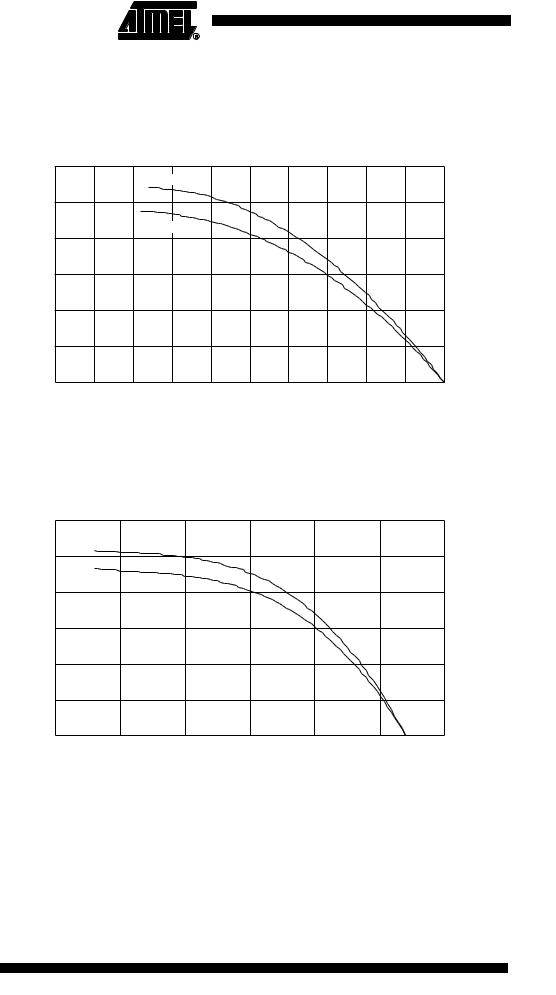
Analog comparator offset voltage is measured as absolute offset.
Figure 51. Analog Comparator Offset Voltage vs. Common Mode Voltage (VCC = 5V)
|
18 |
|
|
|
|
|
|
|
|
|
|
|
16 |
|
|
|
|
|
|
|
|
|
|
|
14 |
|
|
|
|
|
|
|
TA = 25˚C |
|
|
|
|
|
|
|
|
|
|
|
|
|
|
(mV) |
12 |
|
|
|
|
|
|
|
|
TA = 85˚C |
|
|
|
|
|
|
|
|
|
|
|
||
Voltage |
10 |
|
|
|
|
|
|
|
|
|
|
8 |
|
|
|
|
|
|
|
|
|
|
|
Offset |
|
|
|
|
|
|
|
|
|
|
|
6 |
|
|
|
|
|
|
|
|
|
|
|
|
|
|
|
|
|
|
|
|
|
|
|
|
4 |
|
|
|
|
|
|
|
|
|
|
|
2 |
|
|
|
|
|
|
|
|
|
|
|
0 |
|
|
|
|
|
|
|
|
|
|
|
0 |
0.5 |
1 |
1.5 |
2 |
2.5 |
3 |
3.5 |
4 |
4.5 |
5 |
Common Mode Voltage (V)
61
1062G–AVR–01/06

Figure 52. Analog Comparator Offset Voltage vs. Common Mode Voltage (VCC = 2.7V)
|
10 |
|
|
|
|
|
|
|
|
|
|
|
|
TA = 25˚C |
|
|
8 |
|
|
|
|
|
|
(mV) |
6 |
|
|
|
|
|
|
Voltage |
|
|
|
|
|
TA = 85˚C |
|
|
|
|
|
|
|
||
|
|
|
|
|
|
|
|
Offset |
4 |
|
|
|
|
|
|
|
|
|
|
|
|
|
|
|
2 |
|
|
|
|
|
|
|
0 |
|
|
|
|
|
|
|
0 |
0.5 |
1 |
1.5 |
2 |
2.5 |
3 |
Common Mode Voltage (V)
Figure 53. Analog Comparator Input Leakage Current (VCC = 6V; TA = 25°C)
|
60 |
|
|
|
|
|
|
|
|
|
|
|
|
|
|
|
50 |
|
|
|
|
|
|
|
|
|
|
|
|
|
|
|
40 |
|
|
|
|
|
|
|
|
|
|
|
|
|
|
(nA) |
30 |
|
|
|
|
|
|
|
|
|
|
|
|
|
|
|
|
|
|
|
|
|
|
|
|
|
|
|
|
|
|
ACLK |
20 |
|
|
|
|
|
|
|
|
|
|
|
|
|
|
I |
|
|
|
|
|
|
|
|
|
|
|
|
|
|
|
|
10 |
|
|
|
|
|
|
|
|
|
|
|
|
|
|
|
0 |
|
|
|
|
|
|
|
|
|
|
|
|
|
|
|
-10 |
|
|
|
|
|
|
|
|
|
|
|
|
|
|
|
0 |
0.5 |
1 |
1.5 |
2 |
2.5 |
3 |
3.5 |
4 |
4.5 |
5 |
5.5 |
6 |
6.5 |
7 |
VIN (V)
62 ATtiny28L/V
1062G–AVR–01/06

 ATtiny28L/V
Figure 54. Calibrated Internal RC Oscillator Frequency vs. VCC
CALIBRATED RC OSCILLATOR FREQUENCY vs.
OPERATING VOLTAGE
|
1.28 |
|
|
|
|
|
|
|
|
|
1.26 |
|
|
|
|
|
|
TA = 25˚C |
TA = 45˚C |
|
|
|
|
|
|
|
|
||
|
|
|
|
|
|
|
|
|
TA = 70˚C |
|
1.24 |
|
|
|
|
|
|
|
|
|
|
|
|
|
|
|
|
TA = 85˚C |
|
|
1.22 |
|
|
|
|
|
|
|
|
(MHz) |
1.2 |
|
|
|
|
|
|
|
|
1.18 |
|
|
|
|
|
|
|
|
|
Rc |
|
|
|
|
|
|
|
|
|
|
|
|
|
|
|
|
|
|
|
F |
|
|
|
|
|
|
|
|
|
|
1.16 |
|
|
|
|
|
|
|
|
|
1.14 |
|
|
|
|
|
|
|
|
|
1.12 |
|
|
|
|
|
|
|
|
|
1.1 |
|
|
|
|
|
|
|
|
|
2 |
2.5 |
3 |
3.5 |
4 |
4.5 |
5 |
5.5 |
6 |
Vcc(V)
Figure 55. Watchdog Oscillator Frequency vs. VCC
|
1600 |
|
|
|
|
|
|
|
|
|
|
1400 |
|
|
|
|
|
|
TA = 25˚C |
|
|
|
|
|
|
|
|
|
|
|
||
|
1200 |
|
|
|
|
|
|
|
TA = 85˚C |
|
|
|
|
|
|
|
|
|
|
||
(kHz) |
1000 |
|
|
|
|
|
|
|
|
|
800 |
|
|
|
|
|
|
|
|
|
|
RC |
|
|
|
|
|
|
|
|
|
|
|
|
|
|
|
|
|
|
|
|
|
F |
|
|
|
|
|
|
|
|
|
|
|
600 |
|
|
|
|
|
|
|
|
|
|
400 |
|
|
|
|
|
|
|
|
|
|
200 |
|
|
|
|
|
|
|
|
|
|
0 |
|
|
|
|
|
|
|
|
|
|
1.5 |
2 |
2.5 |
3 |
3.5 |
4 |
4.5 |
5 |
5.5 |
6 |
VCC (V)
63
1062G–AVR–01/06
Sink and source capabilities of I/O ports are measured on one pin at a time.
Figure 56. Pull-up Resistor Current vs. Input Voltage (VCC = 5V)
|
120 |
|
|
TA = 25˚C |
|
|
|
|
|
|
|
|
|
|
|
|
|
|
|
|
|
|
|
|
|
|
100 |
|
|
|
|
|
|
|
|
|
|
|
|
|
|
|
|
TA = 85˚C |
|
|
|
|
|
|
|
|
|
80 |
|
|
|
|
|
|
|
|
|
|
(µA) |
|
60 |
|
|
|
|
|
|
|
|
|
|
OP |
|
|
|
|
|
|
|
|
|
|
||
|
|
|
|
|
|
|
|
|
|
|
||
I |
|
|
|
|
|
|
|
|
|
|
|
|
|
|
40 |
|
|
|
|
|
|
|
|
|
|
|
|
20 |
|
|
|
|
|
|
|
|
|
|
|
|
0 |
|
|
|
|
|
|
|
|
|
|
|
|
0 |
0.5 |
1 |
1.5 |
2 |
2.5 |
3 |
3.5 |
4 |
4.5 |
5 |
VOP (V)
Figure 57. Pull-up Resistor Current vs. Input Voltage (VCC = 2.7V)
|
30 |
|
|
|
|
|
|
|
|
|
TA = 25˚C |
|
|
|
|
|
25 |
|
|
|
|
|
|
|
|
|
TA = 85˚C |
|
|
|
|
|
20 |
|
|
|
|
|
|
(µA) |
15 |
|
|
|
|
|
|
OP |
|
|
|
|
|
|
|
|
|
|
|
|
|
|
|
I |
|
|
|
|
|
|
|
|
10 |
|
|
|
|
|
|
|
5 |
|
|
|
|
|
|
|
0 |
|
|
|
|
|
|
|
0 |
0.5 |
1 |
1.5 |
2 |
2.5 |
3 |
VOP (V)
64 ATtiny28L/V
1062G–AVR–01/06

 ATtiny28L/V
Figure 58. I/O Pin Sink Current vs. Output Voltage. All pins except PA2 (VCC = 5V)
|
70 |
|
|
|
TA = 25˚C |
|
|
|
|
|
|
|
|
|
|
|
60 |
|
|
|
|
|
|
|
|
|
|
|
|
TA = 85˚C |
|
|
50 |
|
|
|
|
|
|
(mA) |
40 |
|
|
|
|
|
|
|
|
|
|
|
|
|
|
OL |
|
|
|
|
|
|
|
I |
30 |
|
|
|
|
|
|
|
|
|
|
|
|
|
|
|
20 |
|
|
|
|
|
|
|
10 |
|
|
|
|
|
|
|
0 |
|
|
|
|
|
|
|
0 |
0.5 |
1 |
1.5 |
2 |
2.5 |
3 |
VOL (V)
Figure 59. I/O Pin Source Current vs. Output voltage (VCC = 5V)
|
20 |
|
|
TA = 25˚C |
|
|
|
|
|
|
|
|
|
|
|
|
|
|
|
|
|
|
|
|
18 |
|
|
|
|
|
|
|
|
|
|
|
16 |
|
|
TA = 85˚C |
|
|
|
|
|
|
|
|
|
|
|
|
|
|
|
|
|
|
|
|
14 |
|
|
|
|
|
|
|
|
|
|
(mA) |
12 |
|
|
|
|
|
|
|
|
|
|
10 |
|
|
|
|
|
|
|
|
|
|
|
OH |
|
|
|
|
|
|
|
|
|
|
|
|
|
|
|
|
|
|
|
|
|
|
|
I |
8 |
|
|
|
|
|
|
|
|
|
|
|
|
|
|
|
|
|
|
|
|
|
|
|
6 |
|
|
|
|
|
|
|
|
|
|
|
4 |
|
|
|
|
|
|
|
|
|
|
|
2 |
|
|
|
|
|
|
|
|
|
|
|
0 |
|
|
|
|
|
|
|
|
|
|
|
0 |
0.5 |
1 |
1.5 |
2 |
2.5 |
3 |
3.5 |
4 |
4.5 |
5 |
VOH (V)
65
1062G–AVR–01/06

Figure 60. I/O Pin Sink Current vs. Output Voltage, All Pins Except PA2 (VCC = 2.7V)
|
25 |
|
|
TA = 25˚C |
|
|
|
|
|
|
|
|
20 |
|
|
|
|
|
|
|
|
TA = 85˚C |
|
(mA) |
15 |
|
|
|
|
|
|
|
|
|
|
OL |
|
|
|
|
|
I |
10 |
|
|
|
|
|
|
|
|
|
|
|
5 |
|
|
|
|
|
0 |
|
|
|
|
|
0 |
0.5 |
1 |
1.5 |
2 |
VOL (V)
Figure 61. I/O Pin Source Current vs. Output Voltage (VCC = 2.7V)
|
6 |
|
TA = 25˚C |
|
|
|
|
|
|
|
|
|
|
|
|
|
5 |
|
TA = 85˚C |
|
|
|
|
|
|
|
|
|
|
|
|
|
4 |
|
|
|
|
|
|
(mA) |
3 |
|
|
|
|
|
|
OH |
|
|
|
|
|
|
|
|
|
|
|
|
|
|
|
I |
|
|
|
|
|
|
|
|
2 |
|
|
|
|
|
|
|
1 |
|
|
|
|
|
|
|
0 |
|
|
|
|
|
|
|
0 |
0.5 |
1 |
1.5 |
2 |
2.5 |
3 |
VOH (V)
66 ATtiny28L/V
1062G–AVR–01/06

 ATtiny28L/V
Figure 62. PA2 I/O Pin Sink Current vs. Output Voltage (High Current Pin PA2; TA = 25°C)
|
90 |
|
|
|
|
|
|
|
VCC = 3.6V |
|
|
|
|
|
|
|
|
|
|
|
80 |
|
|
|
|
|
|
|
|
|
70 |
|
|
|
|
VCC = 2.4V |
|
|
|
|
|
|
|
|
|
|
|
|
|
|
60 |
|
|
|
|
|
|
|
|
(mA) |
50 |
|
|
|
|
|
|
|
|
|
|
|
|
|
|
|
|
|
|
OL |
40 |
|
|
|
|
|
|
|
|
I |
|
|
|
VCC = 1.8V |
|
|
|
|
|
|
|
|
|
|
|
|
|
|
|
|
30 |
|
|
|
|
|
|
|
|
|
20 |
|
|
|
|
|
|
|
|
|
10 |
|
|
|
|
|
|
|
|
|
0 |
|
|
|
|
|
|
|
|
|
0 |
0.5 |
1 |
1.5 |
2 |
2.5 |
3 |
3.5 |
4 |
VOL (V)
Figure 63. I/O Pin Input Threshold Voltage vs. VCC (TA = 25°C)
|
2.5 |
|
|
|
2 |
|
|
(V) |
1.5 |
|
|
Voltage |
|
|
|
|
|
|
|
Threshold |
1 |
|
|
|
|
|
|
|
0.5 |
|
|
|
0 |
|
|
|
2.7 |
4.0 |
5.0 |
VCC
67
1062G–AVR–01/06

Figure 64. I/O Pin Input Hysteresis vs. VCC (TA = 25°C)
|
0.18 |
|
|
|
0.16 |
|
|
|
0.14 |
|
|
(V) |
0.12 |
|
|
Hysteresis |
|
|
|
0.1 |
|
|
|
0.08 |
|
|
|
Input |
|
|
|
0.06 |
|
|
|
|
|
|
|
|
0.04 |
|
|
|
0.02 |
|
|
|
0 |
|
|
|
2.7 |
4.0 |
5.0 |
VCC
68 ATtiny28L/V
1062G–AVR–01/06