

Features
•High-performance, Low-power AVR® 8-bit Microcontroller
•RISC Architecture
–118 Powerful Instructions – Most Single Clock Cycle Execution
–32 x 8 General Purpose Working Registers
–Fully Static Operation
–Up to 16 MIPS Throughput at 16 MHz
•Data and Non-volatile Program Memory
–2K Bytes of In-System Programmable Program Memory Flash Endurance: 10,000 Write/Erase Cycles
–128 Bytes of In-System Programmable EEPROM
Endurance: 100,000 Write/Erase Cycles
–128 Bytes Internal SRAM
–Programming Lock for Flash Program and EEPROM Data Security
•Peripheral Features
–8-bit Timer/Counter with Separate Prescaler
–8-bit High-speed Timer with Separate Prescaler
2 High Frequency PWM Outputs with Separate Output Compare Registers Non-overlapping Inverted PWM Output Pins
–Universal Serial Interface with Start Condition Detector
–10-bit ADC
11 Single Ended Channels
8 Differential ADC Channels
7 Differential ADC Channel Pairs with Programmable Gain (1x, 20x)
–On-chip Analog Comparator
–External Interrupt
–Pin Change Interrupt on 11 Pins
–Programmable Watchdog Timer with Separate On-chip Oscillator
•Special Microcontroller Features
–Low Power Idle, Noise Reduction, and Power-down Modes
–Power-on Reset and Programmable Brown-out Detection
–External and Internal Interrupt Sources
–In-System Programmable via SPI Port
–Internal Calibrated RC Oscillator
•I/O and Packages
–20-lead PDIP/SOIC: 16 Programmable I/O Lines
–32-lead QFN/MLF: 16 programmable I/O Lines
•Operating Voltages
–2.7V - 5.5V for ATtiny26L
–4.5V - 5.5V for ATtiny26
•Speed Grades
–0 - 8 MHz for ATtiny26L
–0 - 16 MHz for ATtiny26
•Power Consumption at 1 MHz, 3V and 25°C for ATtiny26L
–Active 16 MHz, 5V and 25°C: Typ 15 mA
–Active 1 MHz, 3V and 25°C: 0.70 mA
–Idle Mode 1 MHz, 3V and 25°C: 0.18 mA
–Power-down Mode: < 1 µA
8-bit  Microcontroller with 2K Bytes Flash
ATtiny26
ATtiny26L
Not recommended for new designs
1477J–AVR–06/07
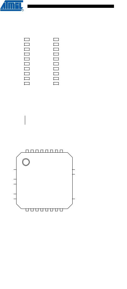
Pin Configuration
PDIP/SOIC
|
|
|
|
|
|
|
(MOSI/DI/SDA/OC1A) PB0 |
1 |
20 |
PA0 (ADC0) |
|||
(MISO/DO/OC1A) PB1 |
2 |
19 |
PA1 (ADC1) |
|||
|
|
|
3 |
18 |
PA2 (ADC2) |
|
(SCK/SCL/OC1B) |
PB2 |
|||||
|
(OC1B) PB3 |
4 |
17 |
PA3 (AREF) |
||
|
|
|
VCC |
5 |
16 |
GND |
|
|
|
GND |
6 |
15 |
AVCC |
(ADC7/XTAL1) PB4 |
7 |
14 |
PA4 (ADC3) |
|||
(ADC8/XTAL2) PB5 |
8 |
13 |
PA5 (ADC4) |
|||
(ADC9/INT0/T0) PB6 |
9 |
12 |
PA6 (ADC5/AIN0) |
|||
|
|
|
|
10 |
11 |
PA7 (ADC6/AIN1) |
(ADC10/RESET) |
PB7 |
|||||
|
|
|
|
|
|
|
NC  1 (OC1B) PB3
  2 NC
2 NC  3 VCC
3 VCC  4 GND
4 GND  5 NC
5 NC  6
6
(ADC7/XTAL1) PB4 
 7 (ADC8/XTAL2) PB5
 8
8
MLF Top View
PB2 (SCK/SCL/OC1B) |
PB1 (MISO/DO/OC1A) |
|
PB0 (MOSI/DI/SDA/OC1A) |
NC |
NC |
NC |
PA0 (ADC0) |
PA1 (ADC1) |
|
||||||||
|
||||||||
32 |
31 |
30 |
29 |
28 |
27 |
26 |
25 |
|
9 |
10 |
11 |
12 |
13 |
14 |
15 |
16 |
|
NC |
PB6 |
|
PB7 |
NC |
PA7 |
PA6 |
PA5 |
NC |
|
(ADC9/INT0/T0) |
|
(ADC10/RESET) |
|
(ADC6/AIN1) |
(ADC5/AIN0) |
(ADC4) |
|
|
|
|
|
|||||
|
|
|
|
|
||||
24  NC
NC
23 
 PA2 (ADC2)
22  PA3 (AREF)
21 
 GND
GND
20  NC
NC
19 
 NC
NC
18  AVCC
AVCC
17 
 PA4 (ADC3)
Note: The bottom pad under the QFN/MLF package should be soldered to ground.
2 ATtiny26(L) 
1477J–AVR–06/07