

147CHAPTER SEVEN
Programmable Logic Devices
Introduction to Programmable Logic
The most common types of programmable logic are two level (AND-OR) logic chips implementing a sum-of-products logic function on each output.
An example sum of products form in standard notation is: F = AB + CDE
The notation used in this book for the example above is: F = A*B + C*D*E. The conventions we will follow include:
•Logic AND is denoted by an asterisk: *
•Logic OR is denoted by a plus sign: +
• Logic inversion (NOT) by a slash: /
The examples above would require three gates: one two-input AND gate, one three-input AND gate and a twoinput OR gate to combine the AND gates’ outputs. (Other references may use different notation, such as & for logic AND, or a minus sign - for inversion, e.g.: F = A & B + -C.)
There are several varieties of two level programmable logic devices, with most of the variations relating to the type of output. Some devices have output flipflops to allow storage and sequential logic, and some have tri-state drivers.
The outputs of some of these devices can be defined at the time they are programmed as inverting, non-inverting, latched, bi-directional, asynchronous and other configurations. The pattern used to program the device is referred to as a fuse map because the original chips used fuse linked memory and the map represents the pattern of blown fuses.
Technologies: Fuse-Link, EPROM, EEPROM, and RAM Storage
Fuse-link PLDs consist of an array of fuses that make connections between the inputs and the logic gates inside the chip. When the chip is programmed, the unwanted fuses are “blown open” to leave only the desired connections. Fuse-link devices are implemented using bipolar logic so they are very fast, and consume a lot of power. Obviously they can only be used once, so they are not as desirable for prototyping purposes as an erasable device. Erasable parts, built using the same technology as EPROM, EEPROM, and RAM data storage for the arrays are available and carry with them the same characteristic advantages and disadvantages as their respective memory types.
148EMBEDDED CONTROLLER
Hardware Design
Architectures
The first user programmable logic array chips had two levels of asynchronous logic. They were organized with two arrays of programmable fuse links, one connecting the inputs to an array of AND gates and the other connecting the AND gate outputs to an array of OR gates driving the output pins. This type of device allows arbitrary sum-of-products logic functions to be implemented limited only by the number of AND and OR gate inputs, and the I/O pins.
Programmable array logic devices are similar to PLA devices except that there is only one fuse array connecting the inputs to the AND gate array. The connections between the AND and OR gates in the PAL are fixed by the design of the PAL. Both PLAs and PALs are made with either active high or active low outputs. It is important to note that the arrays and inputs are not necessarily identical; some OR gates in a PAL may have more inputs than others on the PAL, for example.
Field programmable gate arrays have a more general architecture, and are not limited to the sum-of-products form. FPGAs have programmable interconnecting wires, logic blocks, and I/O pins. The connections and logic in FPGAs are defined by use of either static RAM, E/EEPROM or anti-fuses. Anti-fuses are like fuses, except that they have a high resistance in the unprogrammed state and when programmed their resistance becomes much lower. The antifuse is programmed to make a connection by forcing a current through the anti-fuse. Anti-fuse FPGAs are based on an array of gates and wires that can be selectively shorted with the anti-fuse acting as a one time programmable short circuit. FPGAs are almost exclusively implemented in CMOS technology because of the high logic density to keep the chip power and temperature to reasonable levels. Static RAM based FPGAs are composed of logic blocks with embedded volatile static RAMs that must be loaded with configuration data every time they are powered on. The logic functions and interconnection information is stored in volatile static RAM. The configuration can be loaded from an EPROM or EEPROM directly or via a CPU before they are used.
Relatively large supply currents are drawn by bipolar PLDs, so CMOS versions have been made available to reduce the power consumption requirements. Most of the CMOS PLDs are actually mixed NMOS and CMOS logic, so their power dissipation is not as low as pure CMOS. Use of a PLD in a battery-powered application will generally require a pure CMOS PLD to maximize battery life.
149CHAPTER SEVEN
Programmable Logic Devices
Erasable (E/EE) versions are available from several vendors, which are particularly useful in the development and debug of a new design when things change frequently. The fuses are replaced with floating gate switches with essentially the same construction as the EPROM and EEPROM memory cells described earlier. The EPROM versions of these parts are sold in windowed packages so they can be erased just like a UV EPROM, as well as non-windowed packages that can only be programmed once (one-time programmable, or OTP). The EE versions of these parts are erased electrically before they are programmed.
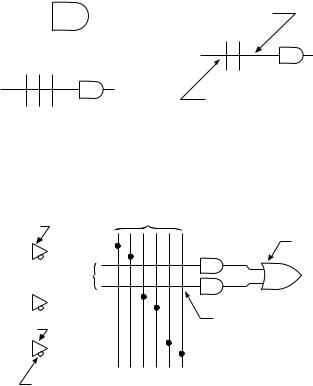
Small programmable logic devices consist of an array of programmable connections, or fuses, interconnecting the input signals with a number of AND gates, followed by an array of connections between the AND gates and some OR gates, resulting in one or more “sum-of-products” logic outputs. The notation used to illustrate the fusible interconnections between the inputs, gates, and outputs
is shown in Figure A |
|
|
|
Programmed |
|
|
|
|
|||
7-1. Its purpose is |
B |
|
|
A • B • C |
(Open) Fuse Link |
|
|
||||
C |
|
|
|
||
|
|
|
|
|
|
to allow a compact |
TTL AND Gate Symbol |
A |
B |
C |
|||||
|
|
|
|
||||||
pictorial represen- |
A |
B |
C |
|
X |
X |
|
A • B |
|
tation of the circuits, |
|
|
|
|
|
||||
|
PLD Representation |
||||||||
|
|
|
|
||||||
by avoiding the |
X |
X |
X |
A • B • C |
|||||
Unprogrammed |
|||||||||
explicit represen- |
|
|
|
|
|||||
PLD Representation |
|
(Intact) Fuse Link |
|||||||
|
|
|
|
|
|
||||
tation of each independent input
signal to gates that have a large number of inputs. Instead of showing every gate input, a single line represents multiple inputs, and an “x” is placed at
points where the gate inputs are connected to one of the PLD input signals. |
|||||||||||||||
Figure 7-2 |
Input Buffer |
|
Input Lines |
||||||||||||
shows an |
|
||||||||||||||
|
|
|
|
|
|
|
2-Wide |
||||||||
|
|
|
|
|
|
|
|
|
|
|
|
||||
example of this. |
A |
|
|
|
|
|
|
|
|
|
|
OR Gate |
|||
|
|
|
|
|
|
|
|
|
|
||||||
|
|
|
|
|
|
|
|
||||||||
In understand- |
|
|
|
|
Product |
X |
|
X |
|
|
|
|
A • B |
||
|
|
|
|
|
|
|
|
|
|
|
|
|
|||
|
|
|
|
Lines |
|
|
|
|
|
|
|
|
|
||
|
|
|
|
X X |
X X X X |
||||||||||
ing how various |
|
|
|
|
|
||||||||||
B |
|
|
|
|
|
|
|
|
|
|
|
|
|
|
|
|
|
|
|
|
|
|
|
|
|
|
|
|
|
||
PLDs operate, |
|
|
|
|
|
|
|
|
|
|
All Fuse Links Intact |
||||
Noninverted |
|
|
|
|
|
|
|
||||||||
it is useful to |
|
|
|
|
|
|
|
||||||||
(True) Path |
|
|
|
|
|
|
|
|
|
|
|||||
look at several |
|
|
|
|
|
|
|
|
|
|
|
||||
C |
|
|
|
|
|
|
|
|
|
|
|
|
|
||
|
|
|
|
|
|
|
|
|
|
|
|
|
|||
ways in which a |
|
|
Inverted |
|
|
|
|
|
|
|
|
|
|
||
programmable |
|
|
(Complement) Path |
|
|
|
|
|
|
|
|||||
logic device can |
Figure 7-2: Simplified PAL logic diagram. |
||||||||||||||
150EMBEDDED CONTROLLER
Hardware Design
be organized. The simplest approach is to use a PROM memory as a programmable logic device, using the address lines as input and the data lines as output.
Figure 7-3 shows a |
|
|
n Inputs |
|
|
|
|
|
||
PROM memory, with |
|
13 |
12 |
11 |
10 |
|
OR Array |
|
||
an array of AND gates |
(Programmable) |
|||||||||
|
|
|
|
|||||||
connected to decode |
|
• |
• |
• |
• |
|
|
|
|
|
each memory address, |
X |
X |
X |
X |
||||||
• |
• |
• |
• |
X |
X |
X |
X |
|||
and multiple bits per |
|
|||||||||
|
• |
• |
• |
• |
X |
X |
X |
X |
||
location that can be |
|
|||||||||
|
• |
• |
• |
• |
X |
X |
X |
X |
||
programmed by the |
|
|||||||||
|
• |
• |
• |
• |
X |
X |
X |
X |
||
user to output an |
|
• |
• |
• |
• |
X |
X |
X |
X |
|
arbitrary binary |
2n |
• |
• |
• |
• |
X |
X |
X |
X |
|
value (memory |
• |
• |
• |
• |
X |
X |
X |
X |
||
Duct |
||||||||||
|
|
|
|
|||||||
contents) for each |
Lines |
• |
• |
• |
• |
X |
X |
X |
X |
|
|
|
|
|
|||||||
combination of the |
|
• |
• |
• |
• |
X |
X |
X |
X |
|
|
• |
• |
• |
• |
X |
X |
X |
X |
||
inputs (addresses). |
|
|||||||||
|
• |
• |
• |
• |
X |
X |
X |
X |
||
|
|
|||||||||
|
|
• |
• |
• |
• |
X |
X |
X |
X |
|
PROM as PLD |
|
• |
• |
• |
• |
X |
X |
X |
X |
|
|
• |
• |
• |
• |
X |
X |
X |
X |
||
Figure 7-3 shows the |
|
• |
• |
• |
• |
X |
X |
X |
X |
|
|
|
AND Array (Fixed) |
|
|
|
|
|
|||
fixed AND array which |
|
|
Q3 |
Q2 |
Q1 |
Q0 |
||||
X = Fuse-Link Crosspoint Connection |
||||||||||
decodes each location in |
n Outputs |
|||||||||
• = Fixed Connection |
|
|||||||||
the PROM. Note the
Figure 7-3: Typical PROM as PLD architecture.
binary pattern of con-
nections in the AND array. The top AND gate decodes address zero, enabling the pattern programmed in the top row of fuses to be presented at the output. This pattern is the 4-bit word of data stored in location zero as a pattern of programmed fuses.
The advantage of using a PROM as a PLD is it can implement any logical function of the inputs, regardless of complexity of the logic function to be represented. This is because each possible permutation of the inputs corresponds to one memory location, and the PROM is essentially a physical implementation of the complete logic truth table. Unfortunately, the number of bits in the memory grows exponentially with the number of inputs. Since most practical logic functions do not have very many product terms on average, the memory is very sparsely filled with data. This means most of the circuitry is effectively wasted.