

Vankka J. - Digital Synthesizers and Transmitters for Software Radio (2000)(en)
.pdf16 |
Chapter 1 |
The delta-coded signals (including image products) are then quadrature upconverted and fed to the two nonlinear power amplifiers. The binary output (±K) from the delta coders results in a carrier phase shift of ± 180° during the upconversion process; this is more commonly known as Phase Reversal Keying (PRK). The resulting upconverted signals are given by
∆IRF (t) |
G ∆I (t)cos(ω0 t) |
|
(1.10) |
∆QRF (t) |
G ∆Q(t)sin(ω0 t), |
where G is the gain of the amplifier. The power amplifiers would be constructed from, for example, class-E stages, with no loss of signal fidelity (since the signals are constant envelope at this point in the system) and with an excellent potential efficiency. Following the nonlinear amplification, the two paths are combined and fed to a bandpass filter. The combination process should, ideally, be lossless, although this is unlikely to be the case in practice. Any imbalance between the two paths should not result in degradation in linearity performance, but will result in an image signal. This image can be arranged to be in-band and hence the suppression required can be relatively modest. As result, a gain and phase error between the two paths of 0.3 dB and 3° may well be adequate for most applications [Ken00]
The bandpass filter (in Figure 1-14) must be sufficiently effective to remove the many out of band products generated by the LIST modulator, and hence is one of the main drawbacks of this technique. Usage of fast digital logic enables a high sampling frequency, so that unwanted products can be
delta |
nonlinear |
|
amplifier |
||
coder |
||
|
I(n)  ∆
∆
local oscillator
|
90 |
|
|
|
|
|
|
|
|
RF output |
||||
|
|
|
|
|
|
|
|
|
|
|
|
fRF |
||
|
|
|
|
|
|
|
|
|
|
|
|
|||
Q(n) |
|
∆ |
|
|
|
|
|
|
|
|
|
|
|
|
|
|
|
|
|
|
|
|
|
|
|
|
|||
|
|
|
|
|
|
|
|
|
|
|
||||
|
delta |
nonlinear |
||||||||||||
|
coder |
|||||||||||||
|
amplifier |
|||||||||||||
|
|
|
|
|
|
|||||||||
Figure 1-14 Basic architecture of a LIST transmitter.
Transmitters |
17 |
pushed far from band, and bandpass filter specifications can be more relaxed.
1.10 Transmitters Based on Bandpass Delta Sigma Modulator
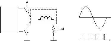
The conventional approach to employing switching mode amplifiers for signals with a time-varying envelope is the class-S amplifier, widely used for audio power amplification. The switching mode amplifier can be implemented as a voltage mode class-D (VMCD) amplifier, schematically shown in Figure 1-15. The signal is passed through a bandpass delta sigma modulator with 1-bit (two-level) output, and the resulting binary signal is fed into a VMCD amplifier. Finally, a bandpass filter is used at the amplifier output prior to the load. The output of the bandpass delta sigma modulator is a binary signal, in which the quantization noise associated with the digitization is spectrally shaped so that it lies largely outside of the band of interest. The output filter provides nonzero conductance essentially only in the band of interest, so there is no power dissipation associated with spectral components that do not reach the load. Amplifiers using the bandpass delta sigma algorithm to generate digital signal streams that encode analog communication signals of interest have also been investigated [Jay98], [Asb99], [Iwa00], and [Key01].
Since the pulse density modulated signal is linear within a narrow bandwidth and the class-D amplifier is a linear stage for digital signals, the filtered output should likewise be linear. With the combination of the bandpass delta sigma modulator and class-D amplifier, this simple amplifier topology has the potential to provide both high linearity and efficiency. A wide bandwidth pre-driver is necessary because the delta sigma modulated signal is broadband, and any significant lowpass and highpass filtering would corrupt the encoded signal. The class-D amplifier (Figure 1-15) has no rejection of errors introduced in the power stage due to power supply modulation, jitter,
VDD
high Q filter
Bandpass |
|
|
out |
|
Delta Sigma
Modulator
∆Σ
Output
Figure 1-15 Schematic structure of voltage mode class-D amplifier, together with representa-
tive output and drive signals.

18 |
Chapter 1 |
switching artifacts, etc.
The principal sources of power loss in the VMCD amplifier (Figure 1-15) are [Ham95], [Jay98]:
1)power lost in the transistors during the ON–OFF transients;
2)energy associated with discharging parasitic capacitance associated with the output terminals of the transistors;
3)power needed to operate the bandpass delta-sigma modulator, and predriver for the output amplifier;
4)power lost in the transistors and diodes associated with their on voltage;
5)power lost in the passive elements, such as the output filter.
The contributions listed as 1)–3) above increase as the rate of switching of the amplifier input increases, and thus require minimizing the sampling frequency of the bandpass delta-sigma modulator. If the entire system is accounted for, the power dissipated by the bandpass delta sigma modulator and the pre-driver has to be considered.
VMCD PAs with power outputs of 100 W to 1 kW are readily implemented at HF, but are seldom used above lower VHF because of losses associated with the drain capacitance [Raa93]. In order to reduce the capacitive loss, the voltage across the switch should be zero when it turns on or off. This is called zero-voltage-switching (ZVS) and can be achieved with current mode class-D (CMCD) amplifiers, where the transistor drain capacitance can become part of the output filter. Another way to reduce turn-on and turn-off loss is minimizing the series inductive loss by zero-current- switching (ZCS), where the current is always zero when the switch turns on or off. The ZCS is, however, less important than the ZVS at hundreds of megahertz switching frequencies [Kob01]. The VMCD power amplifier achieves the ZCS condition. The signal frequency component is only a small
VDD |
VDD |
||||
|
|
Lchoke |
|
|
|
|
|
|
|
||
|
|
|
|
||
|
|
|
|
||
Lchoke |
|||||
|
|||||
load
 high Q filter
Bandpass
Delta Sigma
Modulator
Figure 1-16 Schematic structure of current mode class-D amplifier.

Transmitters |
19 |
I(n) |
|
Interpolation |
|
|
|
|
|
|
|
|
|
|
|
|
|
|
|
|
|
|
|
|
|
||
|
|
|
Filters |
|
|
|
|
|
|
|
|
|
|
|
|
|
|
|
|
|
|
|
|
|
|
|
|
|
|
|
|
|
|
|
|
|
Bandpass |
|
|
|
|
Switching |
|
|
|
Bandpass |
|
||||
|
|
|
|
|
|
|
|
|
|
|
|||||||||||||||
|
|
|
|
|
|
|
NCO |
|
|
|
|
|
|
|
|
|
|
|
|||||||
|
|
|
|
|
|
|
|
Delta Sigma |
|
|
|
Power |
|
|
|
|
|
||||||||
|
|
|
|
|
|
|
|
|
|
|
|
|
|
|
|
|
Filter |
|
|
||||||
|
|
|
|
|
|
|
|
|
|
Modulator |
|
|
|
Amplifier |
|
|
|
|
|
||||||
|
|
|
|
|
|
|
|
|
|
|
|
|
|
|
|
|
|
|
|
||||||
Q(n) |
|
Interpolation |
|
|
|
|
|
|
|
|
|
|
|
|
|
|
|
||||||||
|
|
|
|
|
|
|
|
|
|
|
|
|
|
|
|
|
|
|
|
|
|
||||
Filters
Figure 1-17 Transmitter based on bandpass delta sigma modulator.
portion of the overall ∆¦ modulated signal as shown in Figure 14-8. Therefore the switching frequency is not the same as signal frequency (output filter is tuned to signal frequency), so the drain-to-source currents and drain-to- source voltages have different frequencies; the voltage changes at switching frequency and the current at signal frequency at the VMCD amplifier or vice versa at the CMCD amplifier. Thus, it is impossible to achieve the ZVS or the ZCS when the class-D amplifiers are driven with ∆¦ modulated signals. Only the power at signal frequency is passed to the load, and the switching activity due to the outside band power will cause switching losses. For these reasons, when compared to the square wave with fixed switching frequency, the efficiencies of circuits driven with delta-sigma modulated signals drop dramatically. According to the simulations, the VMCD amplifiers give better efficiency than the CMCD amplifiers with Ȉǻ-modulated signal [Som04]. It is possible to achieve with the VMCD amplifiers high efficiencies at audio frequencies [Var03].
Bandpass delta sigma modulators can be implemented with analog or digital inputs. Figure 1-17 shows the structure of a representative digital transmitter [Spl01].
REFERENCES
[Asb99] P. Asbeck, J. Mink, T. Itoh, and G. Haddad, "Device and Circuit Approaches for Next-Generation Wireless Communications," Microwave J., Vol. 42, No. 2, pp. 22–42, Feb. 1999.
[Bat92] A. Bateman, "The Combined Analogue Locked Loop Universal Modulator (CALLUM)," In Proceedings of the 42nd IEEE Vehicular Technology Conference, May 1992, pp. 759-763.
[Bat98] A. Bateman, and C. K. Yuen, "Method and Apparatus for Amplifying, Modulating and Demodulating," U. S. Patent 5,719,527, Feb. 17, 1998. [Bax01] W. T. Bax, and M. A. Copeland, "A GMSK Modulator Using a Σ∆ Frequency Discriminator-based Synthesizer," IEEE J. Solid-State Circuits, Vol. 36, No. 8, pp. 1218-1227, Aug. 2001.
20 |
Chapter 1 |
[Bax99] W. T. Bax, "Modulation and Frequency Synthesis for Wireless Digital Radio," PhD Thesis, Carleton University, October 1999.
[Cha95] K. Y. Chan, and A. Bateman, "Linear modulators Based on RF synthesis: Realization and Analysis," IEEE Transactions on Circuits and Sys- tems-I: Fundamental Theory and Applications, Vol. 42, No. 6, pp. 321-333, June 1995.
[Che68] E. M. Cherry, and D. E. Hooper, "Amplifying Devices and LowPass Amplifier Design," John Wiley and Sons, Inc., New York, 1968. [Chi35] H. Chireix, "High Power Outphasing Modulation," Proceedings IRE, Vol. 23, No. 11, Nov. 1935, pp. 1370-1392.
[Cox74] D. C. Cox, "Linear Amplification with Nonlinear Components," IEEE Trans. Commun., Vol. COM-22, pp. 1942–1945, Dec. 1974. [Cox75a] D. C. Cox, "Linear Amplification by Sampling Techniques: A New Application for Delta Coders," IEEE Trans. on Comm., Vol. 23, No. 8, pp. 793-798, Aug. 1975.
[Cox75b] D. C. Cox, and R. P. Leck, "Component Signal Separation and Recombination for Linear Amplification with Nonlinear Components," IEEE Transactions on Communications, Vol. 23, pp. 1281-1287, Nov. 1975.
[Dar98] S. Ampem-Darko, and H. S. Al-Raweshidy, "Gain/Phase Imbalance Cancellation Technique in LINC Transmitters," Electron. Lett., Vol. 34, No. 22, pp. 2093–2094, Oct. 1998.
[Das92] M. K. Dasilva, "Vector Locked Loop," U. S. Patent 5,105,168, Apr.
14, 1992.
[Fen97] J. Fenk, "Highly Integrated RF-ICs for GSM and DECT," IEEE Radio Frequency Integrated Circuits (RFIC) Symposium, 1997, pp. 69-72. [Ger01] D. Gerna, A. Giry, D. Manstretta, D. Belot, and D. Pache, "1W 900 MHz Direct Conversion CMOS Transmitter for Paging Applications," RFIC Symposium 2001 Digest of Technical Papers, pp. 191-194.
[Het91] S. A. Hetzel, A. Bateman, and J. P. McGeehan, "LINC Transmitter," Electronics Letters, Vol. 27, No. 10, pp. 844-846, May 1991.
[Irv98] G. Irvine, and et al., "An Up-Conversion Loop Transmitter IC for Digital Mobile Telephones," ISSCC Digest of Technical Papers, Feb. 1998, pp. 364-365.
[Iwa00] M. Iwamoto, A. Jayaraman, G. Hanington, P. F. Chen, A. Bellora, W. Thornton, L. E. Larson, and P. M. Asbeck, "Bandpass Delta-Sigma Class-S Amplifier," Electronics Letters, Vol. 36, 12, pp. 1010-1012, June
2000.
[Jay98] A. Jayaraman, P. F. Chen, G. Hanington, L. Larson, and P. Asbeck, "Linear High-Efficiency Microwave Power Amplifiers Using Bandpass Delta-Sigma Modulators," IEEE Microwave and Guided Wave Letters, Vol. 8, 3, pp. 121–123, March 1998.
Transmitters |
21 |
[Jen98] D. J. Jennings, and J. P. McGeehan, "Hardware Implementation of Optimal CALLUM Transmitter," Electronics Letters, Vol. 34, No. 19, pp. 1816-1817, Sept. 1998.
[Jen99] D. J. Jennings, and J. P. McGeehan, "A High-Efficiency RF Transmitter Using VCO-Derived Synthesis: CALLUM," IEEE Transactions on Microwave Theory and Techniques, Vol. 47, No. 6, June 1999, pp. 715-721. [Kah52] L. R. Kahn, "Single-Sideband Transmission by Envelope Elimination and Restoration," Proceedings IRE, Vol. 40, pp. 803-806, July 1952.
[Ken00] P. B. Kenington, "High-Linearity RF Amplifier Design," Norwood, MA: Artech House, 2000.
[Key01] J. Keyzer, J. Hinrichs, A. Metzger, M. Iwamoto, I. Galton, and P. Asbeck, "Digital Generation of RF Signals for Wireless Communications with Band-Pass Delta-Sigma Modulation," IEEE MTT-S Digest, pp. 2127-
2130, 2001.
[Kob01] H. Kobayashi, J. M. Hinrichs, and P. M. Asbeck, “Current-Mode Class-D Power Amplifiers for High-Efficiency RF Applications,” IEEE Transactions on Microwave Theory and Techniques, Vol. 49, No. 12, pp.
2480–2485, Dec. 2001.
[Lee01] K-Y. Lee, S-W. Lee, Y. Koo, H-K. Huh, H-Y. Nam, J-W. Lee, J. Park, K. Lee, D-K. Jeong, and W. Kim, "Full-CMOS 2.4 GHz Wideband CDMA Transmitter and Receiver with Direct Conversion Mixers and DCOffset Cancellation," Symposium on VLSI Circuits 2001 Digest of Technical Papers, pp. 7-10.
[Liu00] T-P. Liu, and E. Westerwick, "5-GHz CMOS Radio Tranceiver Front-End Chipset," IEEE J. Solid-State Circuits, Vol. 35, pp. 1927-1933, Dec. 2000.
[McM02] D. R. McMahill, and C. G. Sodini, "A 2.5-Mb/s GFSK 5.0-Mb/s 4-FSK Automatically Calibrated Σ∆ Frequency Synthesizer," IEEE J. SolidState Circuits, Vol. 37, No. 1, pp. 18-26, Jan. 2002.
[Nag02] P. J. Nagle, D. P. Burton, E. P. Heaney, and F. J. McGrath, "A Wideband Linear Amplitude Modulator for Polar Transmitters Based on the Concept of Interleaving Delta Modulation," ISSCC Digest of Technical Papers, Feb. 2002, pp. 296-297.
[Ors99] P. Orsatti, F. Piazza, and Q. Huang, "A 20-mA-Receive, 55-mA- Transmit, Single-Chip GSM Tranceiver in 0.25-um CMOS," IEEE J. SolidState Circuits, Vol. 34, pp. 1869-1880, Dec. 1999.
[Per97] M. H. Perrott, T. L. Tewksbury, and C. G. Sodini, "A 27-mW CMOS fractional-N Synthesizer Using Digital Compensation for 2.5-Mb/s GFSK Modulation," IEEE J. Solid-State Circuits, Vol. 32, No. 12, pp. 20482060, Dec. 1997.
[Pet79] V. Petrovic, and W. Gosling, "Polar-loop Transmitter," Electronics Letters, Vol. 15, No. 10, pp. 286-288, May 1979.
22 |
Chapter 1 |
[Pet84] V. Petrovic, and C. N. Smith, "Reduction of Intermodulation Distortion by Means of Modulation Feedback," In IEE Colloquium on Intermodu- lation-Causes, Effects and Mitigation, London, April 9, 1984, pp. 8/ 1-8.
[Raa85] F. H. Raab, "Efficiency of Outphasing RF Power-amplifier Systems," IEEE Transactions on Communications," Vol. 33, No. 10, pp. 10941099, Oct. 1985.
[Raa93] F. H. Raab, and D. J. Rupp, "HF Power Amplifier Operates in Both Class B and Class D," in Proc. RF Expo West, San Jose, CA, Mar. 17–19,
1993, pp. 114–124.
[Raa96] F. H. Raab, "Intermodulation Distortion in Kahn-technique Transmitters," IEEE Trans. On Microwave Theory and Techniques, Vol. 44, No. 12, December 1996, pp. 2273-2278.
[Raa98] F. H. Raab, and et al., "High Efficiency L-band Kahn-technique Transmitter," Proc of IEEE MTT-S, Baltimore, USA, Vol. 2, June 1998, pp. 585-588.
[Raa99] F. H. Raab, "Drive Modulation in Kahn-technique Transmitters," IEEE MTT-S Microwave Symposium Digest, 1999, Vol. 2, pp. 811-814. [Raz98] B. Razavi, "RF Microelectronics," Prentice-Hall PTR, New Jersey, USA, 1998.
[Ril94] T. Riley, and M. Copeland, "A Simplified Continuous Phase Modulator Technique," IEEE Transactions on Circuits and Systems-II, Vol. 41,
No. 5, May 1994, pp. 321-328.
[Rus76] A. J. Rustako, Jr., and Y. S. Yeh, "A Wide-Band Phase-Feedback Inverse-Sine Phase Modulator with Application Toward a LINC amplifier," IEEE Transactions on Communications, Vol. 24, pp. 1139-1143, Oct. 1976. [Shi00] B. Shi, and L. van Sundström, "A 200-MHz IF BiCMOS Signal Component Separator for Linear LINC Transmitters," IEEE J. Solid-State Circuits, Vol. 35, pp. 987–993, July 2000.
[Som04] J. Sommarek, "Digital Modulators with On-Chip D/A Converters," Licentiate’s Thesis, Helsinki University of Technology, 2004.
[Spl01] A. Splett, and et al., "Solutions for Highly Integrated Future Generation Software Radio Basestation Transceivers," in Proc. IEEE Custom Integrated Circuits Conf., 2001, pp. 511-518.
[Sta99] J. Staudinger, and et al., "800 MHz Power Amplifier Using Envelope Following Techniques," Proc. of the IEEE Radio and Wireless Conference (RAWCON) 1999, Denver, Colorado, Aug. 1999, pp. 301-304.
[Su98] D. Su, and W. McFarland, "An IC for Linearizing RF Power Amplifiers Using Envelope Elimination and Restoration," IEEE Journal of SolidState Circuits, Vol. 33, No. 12, Dec. 1998, pp. 2252-2258.
[Sun00] L. Sundström, "Spectral Sensitivity of LINC Transmitters to Quadrature Modulator Misalignments," IEEE Trans. Veh. Technol., Vol. 49, pp. 1474–1487, July 2000.
Transmitters |
23 |
[Sun94] L. Sundström, and M. Johansson, "The Effect of Modulation Scheme on LINC Transmitter Power Efficiency," Electronics Letters, Vol. 30, No. 20, pp. 1643-1645, Sept. 1994.
[Sun95a] L. Sundström, "Automatic Adjustment of Gain and Phase Imbalances in LINC Transmitters," Electronics Letters, Vol. 31, No. 3, pp. 155156, Feb. 1995.
[Sun95b] L. Sundström, "Effects of Reconstruction Filters and Sampling Rate for a Digital Signal Component Separator on LINC Transmitter Performance," Electron. Lett., Vol. 31, No. 14, pp. 1124–1125, July 1995.
[Tom89] S. Tomisato, K. Chiba, and K. Murota, "Phase Error Free LINC Modulator," Electronic Letters, Vol. 25, No. 9, pp. 576-577, Apr. 1989. [Var03] J. Varona, A. A. Hamoui, and K. Martin "A Low-Voltage FullyMonolithic ∆¦ Based Class-D Audio Amplifier " in Proc. ESSCIRC’03, Sept. 2003, pp. 545-548.
[Yam97] T. Yamawaki, and et al., "A 2.7-V GSM RF Transceiver IC," IEEE J. Solid-State Circuits, Vol. 32, pp. 2089-2096, Dec. 1997.
[Zha00] X. Zhang, and L. E. Larson, "Gain and Phase Error Free LINC Transmitter," IEEE Trans. Veh. Technol., Vol. 49, pp. 1986–1994, Sept.
2000.
[Zha01] X. Zhang, L. E. Larson, and P. M. Asbeck, "Calibration Scheme for LINC Transmitter," Electron. Lett., Vol. 37, No. 5, pp. 317–318, Mar. 2001.
Chapter 2
2. POWER AMPLIFIER LINEARIZATION
Traditionally, constant envelope modulation schemes have been used in radio telecommunications because of their simplicity and robustness to amplitude errors. This made it possible to use high efficiency power amplifiers (PA), which are intrinsically very nonlinear devices, near the saturation region where the amplifier efficiency is at its peak.
However these modulation schemes are spectrally inefficient and the current trend is to improve the spectral efficiency or the number of bits transmitted per bandwidth by using some linear modulation scheme such as quadrature amplitude modulation (QAM). Alas, when driven through a nonlinear device the fluctuating envelope of the linear modulation schemes cause intermodulation products to appear around the signal band. This spectral spillage is effectively impossible to filter away and so can cause the amplified signal to exceed its allowed adjacent channel interference (ACI) limits.
To compensate these unwanted effects, various amplifier linearization techniques have been presented. Table 2-1 shows a comparison between three basic linearization techniques, namely, Cartesian feedback, feedforward and predistortion. The cancellation performance of the Cartesian feedback is good, but the bandwidth is narrow, making the technique unsuitable for very wideband systems. The feedforward, on the other hand, can be employed for wideband linearization, but, unfortunately, the system is extremely complicated, resulting in great power waste and large physical size. The third method, predistortion, is an optimal solution in terms of power added efficiency and physical size.
2.1 Feedforward
In the 1920s, H. S. Black invented two schemes for reducing amplifier distortion, namely, feedforward [Bla28] and negative feedback [Bla37]. Feed-

26 |
Chapter 2 |
forward became forgotten in favor of the feedback technique, even though feedforward predated the latter by several years. Today, we are well aware of the limitations of feedback owing to the work of Nyquist and Bode. Feedback is limited by conditional stability and finite inter-modulation distortion (IMD) suppression, whereas feedforward is unconditionally stable and can, in theory, completely eliminate the IMD. However, Black himself noted that the key problem with his feedforward prototype was the primary reason for feedforward to be relegated to the background.
The feedforward prototype required perfect gain match in the different signal paths and Black reported that the gain of the amplifier had to be constantly re-adjusted. Another reason, at that time, was the simple fact that the complexity of the feedforward system compared with negative feedback was considered as a major disadvantage. However, as applications with higher frequencies and bandwidths appeared, the disadvantages of negative feedback became more apparent. This has to some extent led to a renaissance of the feedforward technique and it is nowadays considered to be one of the most established and approved methods, especially for wideband and multicarrier systems [Ken91a], [Ken91b], [Mye94]. Otherwise, it has been used in many areas spanning from low frequency audio applications [Van80] to high-frequency CATV [Pro80] and microwave [Se71b] applications.
A block diagram of the feedforward system is depicted in Figure 2-1. All blocks operate at RF. The main amplifier, a nonlinear power amplifier, is fed directly with the source signal. The distortion generated by the amplifier is isolated in the signal cancellation loop by subtracting the source signal from the amplifier output. This signal is often referred to as the error signal. In the distortion cancellation loop, the error signal is finally subtracted from the amplifier output. For perfect signal and distortion cancellation, an attenuator and auxiliary amplifier are required in the signal and distortion cancellation loops, respectively. For high frequency applications, it is evident that the performance of this scheme in terms of obtaining perfect signal and distortion cancellation is not only dependent on the amplitude match but also on the phase/delay match along the parallel signal arms. In practice, fixed delays can be inserted as noted in Figure 2-1 to balance the delays in the coarms that are primarily dominated by the amplifiers.
The effects of delay, phase and amplitude imbalances have been treated
Table 2-1. Comparison of Three Basic Linearization Techniques [Mad99]
Technique |
Cancel- |
Bandwidth |
Power |
Size |
Suitability to |
|
lation Per- |
|
Added |
|
Multicarrier |
|
fomance |
|
Efficiency |
|
|
Feedback |
Good |
Narrow |
Medium |
Medium |
Low |
Feedforward |
Good |
Wide |
Low |
Large |
High |
Predistortion |
Medium |
Medium |
High |
Small |
Medium |