

03.Combinational circuits
.pdfChapter 3 − Combinational Circuits |
Page 11 of 26 |
F |
yz |
|
|
x' |
|
|
|
|
|
||
x |
|
00 |
01 |
11 |
10 |
|
0 |
1 |
1 |
1 |
1 |
|
1 |
|
|
|
|
(a)
F |
yz |
|
|
z' |
|
|
|
|
|
||
x |
|
00 |
01 |
11 |
10 |
|
0 |
1 |
|
|
1 |
|
1 |
1 |
|
|
1 |
(d)
F |
yz |
|
|
z |
|
|
|
|
|
||
x |
|
00 |
01 |
11 |
10 |
|
0 |
|
1 |
1 |
|
|
1 |
|
1 |
1 |
|
(b)
F |
|
|
x'z' |
|
yz |
|
|
|
|
wx |
00 |
01 |
11 |
10 |
00 |
1 |
|
|
1 |
01 |
|
|
|
|
11 |
|
|
|
|
10 |
1 |
|
|
1 |
F |
yz |
|
|
y'z |
|
|
|
|
|
|
|
wx |
|
00 |
01 |
11 |
10 |
|
00 |
|
1 |
|
|
|
01 |
|
1 |
|
|
|
11 |
|
1 |
|
|
|
10 |
|
1 |
|
|
|
|
|
(c) |
|
|
F |
yz |
|
x'y' |
|
x'z |
|
|
|
|||
x |
|
00 |
01 |
11 |
10 |
y'z |
0 |
1 |
1 |
1 |
|
1 |
|
1 |
|
|
|
|
|
|
|
||
|
|
|
(f) |
|
|
(e)
Figure 4. (a) to (e) examples of 2-subcubes in 3-variable and 4-variable K-maps; (f) cannot form a 2-subcube
F |
y |
|
x' |
|
|
|
|
||
|
x |
0 |
1 |
|
|
0 |
0 |
1 |
1 |
|
1 |
|
||
|
|
2 |
|
3 |
|
1 |
|
1 |
y |
|
|
|
The 1-minterms m0 (x'y') and m1 (x'y) are adjacent to each other, which means that they differ in the value of only one variable. In this case, x is 0 for both minterms, but y is 0 for one and 1 for the other. Thus, variable y is dropped and the two terms are combined together giving just x'. This reasoning corresponds to the expression
x'y' + x'y = x' (y'+y) = x'
Similarly, the 1-minterms m1 (x'y) and m3 (xy) are also adjacent and y is the variable having the same value for both minterms, and so they can be combined to give
x'y + xy = y
We use the term subcube to refer to a rectangle of adjacent 1-minterms. These subcubes must be rectangular in shape and can only have sizes that are the powers of two. Formally, for an n-variable K-map, an m-subcube is defined as that set of 2m minterms in which n – m of the variables will have the same value in every minterm while the remaining variables will take on the 2m possible combinations of 0’s and 1’s. Thus, a 1-minterm all by itself is called a 0-subcube, and two adjacent 1-minterms is a 1-subcube. In the above 2-variable K-map, there are two 1- subcubes: one label with x' and one with y. A 2-subcube will have four adjacent 1-minterms and can be in the shape of any one of those in Figure 4 (a) to (e).
Notice that Figure 4 (d) and (e) also form 2-subcubes even though the four 1-minterms are not physically adjacent to each other. They are adjacent, however, because the first and last rows, and first and last columns wrap around in a K-map. In Figure 4 (f), the four 1-minterms cannot form a 2-subcube because they do not form a rectangle. However, they can form three 1-subcubes – y'z, x'y' and x'z.
Microprocessor Design – Principles and Practices with VHDL |
Last updated 7/17/2003 5:56 PM |

Chapter 3 − Combinational Circuits |
Page 12 of 26 |
We say that a subcube is characterized by the variables having the same values for all the minterms in that subcube. In general, an m-subcube for an n-variable K-map will be characterized by n – m variables. If the value that is similar for all the variables is a 1, that variable is unprimed, whereas, if the value that is similar for all the variables is a 0, that variable is primed. In an expression, this is equivalent to the resulting smaller product term when the minterms are combined together. For example, the 2-subcube in Figure 4 (d) is characterized by z' since the value of z is 0 for all the minterms, whereas the values for x and y are not all the same for all the minterms. Similarly, the 2-subcube in Figure 4 (e) is characterized by x'z'.
For a 5-variable K-map as in Figure 3 (d), we need to visualize the right half of the array where v = 1 to be on top of the left half where v = 0. Thus, for example, minterm 20 is adjacent to minterm 4, and minterm 31 is adjacent to minterm 15.
The K-map method reduces a Boolean function from its canonical form to its standard form. The goal for the K- map method is to find as few subcubes as possible to cover all the 1-minterms in the given function. This naturally implies that the subcube size should be as big as possible. The reasoning is that each subcube gives a product term and all the subcubes (or product terms) must be ORed together to give the function. Larger subcubes require fewer AND gates because of fewer variables in the product term, and fewer subcubes will require fewer OR gates.
The procedure for using the K-map method is as follows:
1.Draw the appropriate K-map for the given function and place a 1 in the squares that correspond to the function’s 1-minterms.
2.For each 1-minterm, find the largest subcube that covers this 1-minterm. This largest subcube is known as a prime implicant (PI). By definition, a prime implicant is a subcube that is not contained within any other subcube. If there are more than one subcube that is the same size as the largest subcube, then they are all prime implicants.
3.Look for 1-minterms that are covered by only one prime implicant. Since this prime implicant is the only subcube that covers this particular 1-minterm, this prime implicant is a must have in the final solution. This prime implicant is referred to as an essential prime implicant (EPI). By definition, an essential prime implicant is a subcube that includes a 1-minterm that is not included in any other subcube.
4.Create a minimal cover list by selecting the smallest possible number of prime implicants such that every 1- minterm is contained in at least one prime implicant. This cover list must include all the essential prime implicants plus zero or more of the remaining prime implicants. It is alright that a particular 1-minterm is covered in more than one prime implicant, but all 1-minterms must be covered.
5.The final minimized function is obtained by ORing all the prime implicants from the minimal cover list.
Note that the final minimized function obtained by the K-map method may not be in its most reduced form. It is only in its most reduced standard form. Sometimes, it is possible to reduce the standard form further into a nonstandard form.
Example 3.3
Use the K-map method to minimize a 4-variable (w, x, y and z) function F with the 1-minterms: m0, m2, m5, m7, m10, m13, m14, and m15. We start with the following 4-variable K-map
F |
yz |
|
|
|
|
|
|
|
|
|
|
wx |
|
00 |
01 |
11 |
10 |
|
00 |
0 |
1 |
3 |
2 |
|
1 |
|
|
1 |
|
|
01 |
4 |
5 |
7 |
6 |
|
|
1 |
1 |
|
|
|
11 |
12 |
13 |
15 |
14 |
|
|
1 |
1 |
1 |
|
|
10 |
8 |
9 |
11 |
10 |
|
|
|
|
1 |
Microprocessor Design – Principles and Practices with VHDL |
Last updated 7/17/2003 5:56 PM |

Chapter 3 − Combinational Circuits |
Page 13 of 26 |
The prime implicants for each of the 1-minterms are shown in the following K-map and table:
F |
|
|
w'x'z' |
|
yz |
|
|
|
|
|
|
|
|
|
wx |
00 |
01 |
11 |
10 |
00 |
1 |
|
|
1 |
01 |
|
1 |
1 |
x'yz' |
11 |
|
1 |
1 |
1 |
|
|
|
|
wyz' |
10 |
|
|
|
1 |
|
xz |
|
wxy |
|
1-minterm |
Prime Implicant |
m0 |
w'x'z' |
m2 |
w'x'z', x'yz' |
m5 |
xz |
m7 |
xz |
m10 |
x'yz', wyz' |
m13 |
xz |
m14 |
wyz', wxy |
m15 |
xz |
|
|
Thus, there are five prime implicants: w'x'z', x'yz', xz, wyz', and wxy. Of these five prime implicants, w'x'z' and xz are essential prime implicants since m0 is covered only by w'x'z', and m5, m7, and m13 are covered only by xz.
We start the cover list by including the two essential prime implicants w'x'z' and xz. These two subcubes will have covered minterms m0, m2, m5, m7, m13 and m15. To cover the remaining two uncovered minterms m10 and m14, we want to use as few prime implicants as possible. Hence, we select the prime implicant wyz' which covers both of them.
Finally, our reduced standard form equation is obtained by ORing these three prime implicants
F = w'x'z' + xz + wyz'.
Notice that we can reduce this standard form equation even further by factoring out the z' from the first and last term to get the non-standard form equation
F = z' (w'x' + wy) + xz. |
♦ |
Example 3.4
Use the K-map method to minimize a 5-variable function F (v, w, x, y and z) with the 1-minterms: v'w'x'yz', v'w'x'yz, v'w'xy'z, v'w'xyz, vw'x'yz', vw'x'yz, vw'xyz', vw'xyz, vwx'y'z, vwx'yz, vwxy'z, and vwxyz.
F |
|
|
|
w'x'y |
w'yz |
|
||
yz |
|
v = 0 |
|
|
|
v = 1 |
|
|
|
|
|
|
|
|
|||
wx |
00 |
01 |
11 |
10 |
00 |
01 |
11 |
10 |
|
00 |
|
1 |
1 |
|
|
1 |
1 |
v'w'xz |
01 |
1 |
1 |
|
|
|
1 |
1 |
11 |
|
|
|
|
|
|
vw'y |
|
|
|
|
|
|
1 |
1 |
||
|
|
|
|
|
|
|||
|
10 |
|
|
|
|
1 |
1 |
|
|
|
|
|
|
vwz |
|
|
vyz |
The list of prime implicants is: v'w'xz, w'x'y, w'yz, vw'y, vyz, and vwz. From this list of prime implicants, w'yz and vyz are not essential. The four remaining essential prime implicants are able to cover all the 1-minterms. Hence the solution in standard form is
F = v'w'xz + w'x'y + vw'y + vwz |
♦ |
3.4.2 Don’t-cares
There are times when a function is not fully specified. In other words, there are some minterms for the function where we do not care whether their values are a 0 or a 1. When drawing the K-map for these “don’t-care” minterms, we assign an “× ” in that square instead of a 0 or a 1. Usually, a function can be reduced even further if we
Microprocessor Design – Principles and Practices with VHDL |
Last updated 7/17/2003 5:56 PM |

Chapter 3 − Combinational Circuits |
Page 14 of 26 |
remember that these × ’s can be either a 0 or a 1. As you recall when drawing K-maps, enlarging a subcube reduces the number of variables for that term. Thus, in drawing subcubes, some of them may be enlarged if we treat some of these × ’s as 1’s. On the other hand, if some of these × ’s will not enlarge a subcube, then we want to treat them as 0’s so that we do not need to cover them. It is not necessary to treat all × ’s to be all 1’s or all 0’s. We can assign some × ’s to be 0’s and some to be 1’s.
For example, given a function having the following 1-minterms and don’t-care minterms: 1-minterms: m0, m1, m2, m3, m4, m7, m8 and m9.
× -minterms: m10, m11, m12, m13, m14 and m15.
we obtain the following K-map with the prime implicants x', yz and y'z'.
F |
yz |
|
|
|
|
|
|
|
|
|
|
|
|
|
|
|
|
|
|
|
|
wx |
|
00 |
01 |
11 |
10 |
|
||||
|
00 |
1 |
0 |
1 |
1 |
1 |
3 |
1 |
2 |
|
|
|
|
|
|
x' |
|||||
y'z' |
01 |
1 |
4 |
|
5 |
1 |
7 |
|
6 |
|
12 |
|
13 |
15 |
|
14 |
yz |
||||
|
11 |
× |
× |
× |
× |
|||||
|
10 |
1 |
8 |
1 |
9 |
× |
11 |
× |
10 |
|
Notice that in order to get the 4-subcube characterized by x' the two don’t-care minterms m10 and m11 are taken to have the value 1. Similarly with the minterms m12 and m15. On the other hand, the don’t-care minterms m13 and m14 are taken to have the value 0 so that they do not need to be covered in the solution. The reduced standard form function as obtained from the K-map is, therefore
F = x' + yz + y'z'.
Again, this equation can be reduced further by recognizing that yz + y'z' = y z. Thus,
F= x' + (y z).
3.4.3* Quine-McCluskey (Tabulation) Method
K-maps are useful for manually obtaining the minimized standard form Boolean function for may be up to at most six variables. However, for functions with more than six variables, it becomes very difficult to visualize how the minterms should be combined into subcubes. Moreover, the K-map algorithm is not as straight forward to program the computer with. There exist tabulation methods, one of which is the Quine-McClusky method that are better suited for programming the computer, and thus can solve any function having any number of variables.
Example 3.4
We now illustrate the Quine-McClusky algorithm using the same four-variable function as in example 3.2 and repeated here
f(w,x,y,z) = Σ (0,2,5,7,10,13,14,15)
To construct the initial table, the minterms are grouped according to the number of 1’s in that minterm number’s binary representation. For example, m0 (0000) has no 1’s; m2 (0010) has one 1; m5 (0101) has two 1’s; etc. Thus, the initial table of 0-subcubes (i.e. subcubes having only one minterm) as obtain from the above function is
Microprocessor Design – Principles and Practices with VHDL |
Last updated 7/17/2003 5:56 PM |
Chapter 3 − Combinational Circuits |
|
|
|
|
|
|
Page 15 of 26 |
|
|
|
|
|
|
|
|
|
|
|
Group |
Subcube |
Subcube Value |
Subcube |
||||
|
Minterms |
w |
x |
y |
z |
Covered |
|
|
|
|
|
||||||
|
G0 |
m0 |
0 |
0 |
0 |
0 |
|
|
|
G1 |
m2 |
0 |
0 |
1 |
0 |
|
|
|
G2 |
m5 |
0 |
1 |
0 |
1 |
|
|
|
|
m10 |
1 |
0 |
1 |
0 |
|
|
|
G3 |
m7 |
0 |
1 |
1 |
1 |
|
|
|
|
m13 |
1 |
1 |
0 |
1 |
|
|
|
|
m14 |
1 |
1 |
1 |
0 |
|
|
|
G4 |
m15 |
1 |
1 |
1 |
1 |
|
|
The “Subcube Covered” column is filled in from the next step.
In the second step, we construct a second table by combining those minterms in adjacent groups from the first table that differ in only one bit position. For example, m0 and m2 differ in only the y bit. Thus, this table lists all the 1-subcubes. A hyphen (–) is used in the bit position that is different in the two minterms. Since this 1-subcube covers the two individual minterms, we make a note of it by checking the two minterms in the “Subcube Covered” column in the previous table. The 1-subcube table is shown next
Group |
Subcube |
Subcube Value |
Subcube |
||||
Minterms |
w |
x |
y |
z |
Covered |
||
|
|||||||
G0 |
m0,m2 |
0 |
0 |
– |
0 |
|
|
G1 |
m2,m10 |
– |
0 |
1 |
0 |
|
|
G2 |
m5,m7 |
0 |
1 |
– |
1 |
|
|
|
m5,m13 |
– |
1 |
0 |
1 |
|
|
|
m10,m14 |
1 |
– |
1 |
0 |
|
|
G3 |
m7,m15 |
– |
1 |
1 |
1 |
|
|
|
m13,m15 |
1 |
1 |
– |
1 |
|
|
|
m14,m15 |
1 |
1 |
1 |
– |
|
|
We repeat the second step as long as there are adjacent subcubes that differ in only one bit position including the hyphen. These subcubes are combined to give the next subcube table. From the above 1-subcube table, we get the following 2-subcube table
Group |
Subcube |
Subcube Value |
Subcube |
||||
Minterms |
w |
x |
y |
z |
Covered |
||
|
|||||||
G2 |
m5,m7,m13,m15 |
– |
1 |
– |
1 |
|
|
We stop when there are no more subcubes that can be combined. The prime implicants are those subcubes that are not covered, i.e. those without a check mark in the Subcube Covered column. For example, from the last table (2-subcube table) the only subcube in this table has the value x = 1 and z = 1, thus we get the prime implicant xz. From the 1-subcube table, we have the four prime implicants w'x'z', x'yz', wyz', and wxy. Note that these prime implicants may not necessary be all in the last table. These five prime implicants are exactly the same as those obtained in example 3.2.
3.5* Timing Hazards and Glitches
As you probably know, things in practice don’t always work according to what you learn in school. Hazards and glitches in circuits are such examples. In our analysis of combinational circuits, we have only been performing a functional analysis. A functional analysis assumes that there is no delay for signals to pass from the input to the output of a gate. In other words, we look at a circuit only with respect to its logical operation as defined by the Boolean Theorems. We have not considered the timing of the circuit. When a circuit is actually implemented, the timing of the circuit, that is, the time for the signals to pass from the input of a logic gate to the output, is very critical and must be treated with care. Otherwise, an actual implementation of the circuit may not work according to the functional analysis of the same circuit. Timing hazards are problems in a circuit as a result of timing issues.
Microprocessor Design – Principles and Practices with VHDL |
Last updated 7/17/2003 5:56 PM |
Chapter 3 − Combinational Circuits |
Page 16 of 26 |
These problems can be observed only from a timing analysis of the circuit or from an actual implementation of the circuit. A functional analysis of the circuit will not reveal timing hazard problems.
A glitch is when a signal is expected to be stable (from a functional analysis) but it changes value for a brief moment and then goes back to what it is expected to be. For example, if a signal is expected to be at a stable 0, but instead, it goes up to a 1 and then drops back to a 0 very quickly. This sudden unexpected transition of the signal is a glitch, and the circuit having this behavior contains a hazard.
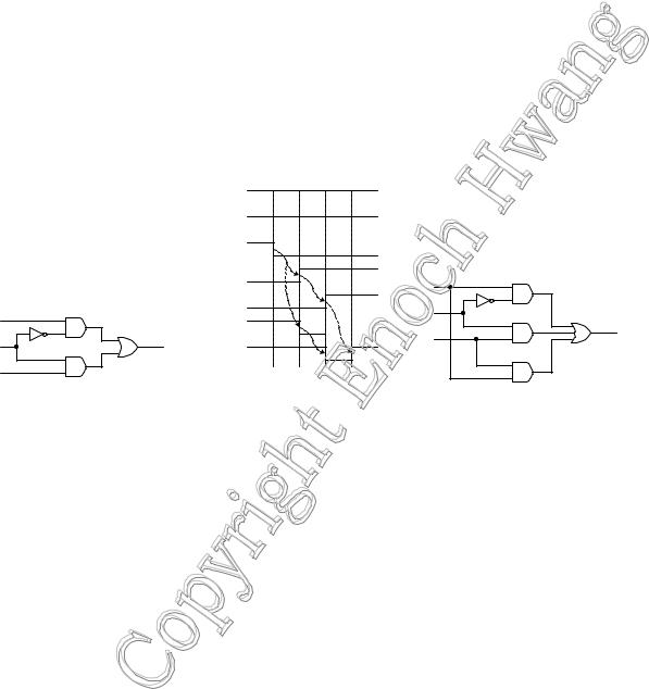
Take, for example, the simple 2-to-1 multiplexer circuit shown in Figure 5 (a). If both d0 and d1 are at a constant 1, and lets assume that s goes from a 1 to a 0. For a functional analysis of the circuit, the output y should remain at a constant 1. However, if we perform a timing analysis of the circuit, we will see something different in the timing diagram. Let as assume that all the logic gates in the circuit have a delay of one time unit. The resulting timing trace is shown in Figure 5 (b). At time t0, s drops to a 0. Since it takes one time unit for s to be inverted through the inverter, s' changes to a 1 after one time unit at time t1. At the same time, it takes the bottom AND gate one time unit for the output to change to a 0 at time t1. However, the top AND gate will not see any input change until time t1, and when it does, it takes another one time unit for its output s'd0 to rise to a 1 at time t2. Starting at time t1, both inputs of the OR gate is a 0, so after one time unit, the OR gate outputs a 0 at time t2. At time t2 when the top AND gate outputs a 1, the OR gate will take this 1 input and outputs a 1 after one time unit at t3. So between times t2 and t3, output y unexpectedly drops to a 0 for one time unit and then rises back to a 1. Hence, the output signal y has a glitch and the circuit has a hazard.
As you may have noticed, glitches in a signal are caused by multiple sources having paths of different delays driving that signal. To prevent glitches from occurring, one method is to add redundant circuitry. Figure 5 (c) shows a functionally correct 2-to-1 multiplexer. However, with the extra AND gate, no glitches can occur. These types of simple glitches can be easily solved using K-maps.
|
|
|
|
d0 |
|
|
|
|
|
|
|
|
d1 |
|
|
|
|
|
|
|
|
s |
|
|
|
|
|
|
|
|
s' |
|
|
|
d0 |
|
|
|
|
s'd0 |
|
|
|
|
|
|
|
|
|
|
|
s |
|
d0 |
|
s'd0 |
|
sd1 |
|
|
|
|
|
|
|
|
|
y |
|||
s |
s' |
|
y |
|
|
|
||
|
y |
|
|
|
d1 |
|||
|
|
|
|
|
|
|
|
|
d1 |
|
sd1 |
|
|
t0 |
t1 |
t2 |
t3 |
(a) |
(b) |
(c) |
Figure 5. Example of a glitch: (a) 2-to-1 multiplexer circuit; (b) timing trace; (c) 2-to-1 multiplexer circuit with no glitches.
3.67-Segment Decoder Example
We will now synthesize the circuit for a 7-segment decoder for driving a 7-segment LED display. The 7- segment decoder converts a 4-bit input to seven output lines for turning on the seven lights in a 7-segment LED display. The 4-bit input encodes the binary representation of a decimal digit. Given the decimal digit input, the seven output lines are turned on in such a way so that the LED displays the corresponding digit. The 7-segment LED display schematic with the names of each segment labeled is shown below
Microprocessor Design – Principles and Practices with VHDL |
Last updated 7/17/2003 5:56 PM |

Chapter 3 − Combinational Circuits |
Page 17 of 26 |
a
f g b
e c
d
The operation of the 7-segment decoder is specified in the truth table in Figure 6. The four inputs to the decode are I3, I2, I1, and I0, and the seven outputs for each of the seven LEDs are labeled seg a, seg b, …, seg g. For each input combination, the corresponding digit to display on the 7-segment LED is shown in the Display column. The segments that need to be turned on for that digit will have a 1 while the segments that need to be turned off for that digit will have a 0. For example, for the 4-bit input 0000, which corresponds to the digit 0, segments a, b, c, d, e and f need to be turned on while segment g needs to be turned off.
Notice that the input combinations 1010 to 1111 are not used and so don’t care values are assigned to all the segments for these six combinations.
|
Inputs |
|
Decimal |
|
|
|
|
seg a |
seg b |
seg c |
seg d |
seg e |
seg f |
seg g |
|||||||||||
I3 |
I2 |
I1 |
I0 |
digit |
Display |
|
|
|
|
|
|
|
|
|
|
|
|
|
|
|
|
|
|||
|
|
|
|
|
|
|
|
|
|
|
|
|
|
|
|
||||||||||
|
|
|
|
|
|
|
|
|
|
|
|
|
|
|
|
||||||||||
|
|
|
|
|
|
|
|
|
|
|
|
|
|
|
|
|
|
|
|
|
|||||
0 |
0 |
0 |
0 |
0 |
|
|
|
|
1 |
|
1 |
|
1 |
|
1 |
|
1 |
1 |
0 |
|
|||||
|
|
|
|
|
|
|
|
|
|||||||||||||||||
|
|
|
|
|
|
|
|
|
|
|
|
|
|
|
|
|
|
|
|
|
|||||
0 |
0 |
0 |
1 |
1 |
|
|
|
|
0 |
|
1 |
|
1 |
|
0 |
|
0 |
0 |
0 |
|
|||||
|
|
|
|
|
|
|
|
|
|
|
|
|
|
|
|
|
|
|
|
|
|||||
0 |
0 |
1 |
0 |
2 |
|
|
|
|
1 |
|
1 |
|
0 |
|
1 |
|
1 |
0 |
1 |
|
|||||
|
|
|
|
|
|
|
|
|
|||||||||||||||||
|
|
|
|
|
|
|
|
||||||||||||||||||
|
|
|
|
|
|
|
|
|
|
|
|
|
|
|
|
|
|
|
|
||||||
0 |
0 |
1 |
1 |
3 |
|
|
|
|
1 |
|
1 |
|
1 |
|
1 |
|
0 |
0 |
1 |
|
|||||
|
|
|
|
|
|
|
|
||||||||||||||||||
|
|
|
|
|
|
||||||||||||||||||||
|
|
|
|
|
|
|
|
|
|
|
|
|
|
|
|
|
|
|
|
||||||
0 |
1 |
0 |
0 |
4 |
|
|
|
|
0 |
|
1 |
|
1 |
|
0 |
|
0 |
1 |
1 |
|
|||||
|
|
|
|
|
|
|
|
||||||||||||||||||
|
|
|
|
|
|
||||||||||||||||||||
|
|
|
|
|
|
|
|
|
|
|
|
|
|
|
|
|
|
|
|
||||||
0 |
1 |
0 |
1 |
5 |
|
|
|
|
1 |
|
0 |
|
1 |
|
1 |
|
0 |
1 |
1 |
|
|||||
|
|
|
|
|
|
|
|
|
|||||||||||||||||
|
|
|
|
|
|
|
|||||||||||||||||||
|
|
|
|
|
|
|
|
|
|
|
|
|
|
|
|
|
|
||||||||
0 |
1 |
1 |
0 |
6 |
|
|
|
|
1 |
|
0 |
|
1 |
|
1 |
|
1 |
1 |
1 |
|
|||||
|
|
|
|
|
|
|
|
|
|||||||||||||||||
|
|
|
|
|
|
|
|
||||||||||||||||||
|
|
|
|
|
|
|
|
|
|
|
|
|
|
|
|
|
|
||||||||
0 |
1 |
1 |
1 |
7 |
|
|
|
|
1 |
|
1 |
|
1 |
|
0 |
|
0 |
0 |
0 |
|
|||||
|
|
|
|
|
|
|
|||||||||||||||||||
|
|
|
|
|
|
|
|
||||||||||||||||||
|
|
|
|
|
|
|
|
|
|
|
|
|
|
|
|
|
|
||||||||
1 |
0 |
0 |
0 |
8 |
|
|
|
|
1 |
|
1 |
|
1 |
|
1 |
|
1 |
1 |
1 |
|
|||||
|
|
|
|
|
|
|
|
||||||||||||||||||
|
|
|
|
|
|
|
|
||||||||||||||||||
|
|
|
|
|
|
|
|
|
|
|
|
|
|
|
|
|
|
|
|
||||||
1 |
0 |
0 |
1 |
9 |
|
|
|
|
1 |
|
1 |
|
1 |
|
0 |
|
0 |
1 |
1 |
|
|||||
|
|
|
|
|
|
|
|
|
|||||||||||||||||
|
|
|
|
|
|
||||||||||||||||||||
|
|
|
|
|
|
|
|
|
|
|
|
|
|
|
|
|
|
||||||||
rest of the combinations |
|
× |
|
× |
|
× |
|
× |
|
× |
× |
× |
|
||||||||||||
Figure 6. Truth table for the 7-segment decoder.
From the truth table, we are able to specify seven equations that are dependent on the four inputs for each of the seven segments. For example, the canonical form equation for segment a is
a = I3'I2'I1'I0' + I3'I2'I1I0' + I3'I2'I1I0 + I3'I2I1'I0 + I3'I2I1I0' + I3'I2I1I0 + I3I2'I1'I0' + I3I2'I1'I0
Before implementing this equation directly in a circuit, we want to simplify it first using the K-map method. The K-map for the equation for segment a is
Microprocessor Design – Principles and Practices with VHDL |
Last updated 7/17/2003 5:56 PM |

Chapter 3 − Combinational Circuits |
Page 18 of 26 |
a |
I1I0 |
|
|
|
|
|
|
|
|
|
|
|
|
|
|
|
|
|
|
|
|
I3I2 |
|
00 |
01 |
11 |
10 |
I2'I0' |
||||
|
00 |
1 |
0 |
|
1 |
1 |
3 |
1 |
2 |
|
|
|
|
|
|
|
I2I0 |
||||
|
01 |
|
4 |
1 |
5 |
1 |
7 |
1 |
6 |
|
|
|
|
|
|
|
I1 |
||||
|
|
|
12 |
|
13 |
|
15 |
|
14 |
|
|
11 |
× |
× |
× |
× |
|
||||
|
10 |
1 |
8 |
1 |
9 |
× |
11 |
× |
10 |
|
I3
From evaluating the K-map, we derive the simpler equation for segment a as
a = I3 + I1 + I2'I0' + I2I0 = I3 + I1 + (I2 I0) Proceeding in a similar manner, we get the following remaining six equations
b= I2' + (I1 I0)
c= I2 + I1' + I0
d= I1I0' + I2'I0' + I2'I1 + I2I1'I0
e= I1I0' + I2'I0'
f= I3 + I2I1' + I2I0' + I1'I0'
g = I3 + (I2 I1) + I1I0'
From these seven simplified equations, we can now implement the circuit as shown in Figure 7.
I3 |
I2 |
I1 |
I0 |
|
|
|
a |
|
|
|
b |
|
|
|
c |
|
|
|
d |
|
|
|
e |
|
|
|
f |
|
|
|
g |
Figure 7. Circuit for the 7-segment decoder.
Microprocessor Design – Principles and Practices with VHDL |
Last updated 7/17/2003 5:56 PM |

Chapter 3 − Combinational Circuits |
Page 19 of 26 |
3.7VHDL Code for Combinational Circuits
Writing VHDL code to describe a circuit, whether combinational or sequential, can be done at any one of three levels: structural, dataflow, or behavioral. At the structural level, which is the lowest level, you have to first manually design the circuit. Having drawn the circuit, you use VHDL to specify the components and gates that are needed by the circuit and how they are connected together by following your circuit exactly. Synthesizing a structural VHDL description of a circuit will, of course, produce a netlist that is exactly like your original circuit. The advantage of working at the structural level is that you have full control as to what components are used and how they are connected. On the other hand, you need to first come up with the circuit and so the full capabilities of the synthesizer are not utilized.
At the dataflow level, you use the built-in logical functions of VHDL in signal assignment statements to describe a circuit, which again you have to first design manually. Boolean functions that describe a circuit can be easily converted to signal assignment statements using the built-in logical functions. The only drawback is that the built-in logical functions such as the AND and OR function only take two operands. This is like having only 2-input gates to work with.
All the statements use in the structural and dataflow level are executed concurrently. As oppose to statements in a computer program, which are usually executed in a sequential manner. In other words, the ordering of the VHDL statements written in the structural or dataflow level does not matter – the result would be exactly the same.
Describing a circuit at the behavioral level is most similar to writing a computer program. You have all the standard high-level programming constructs such as the FOR LOOP, WHILE LOOP, IF THEN ELSE, CASE, and variable assignments. The statements are enclosed in a process block and are executed sequentially.
3.7.1 Structural BCD to 7-Segment Decoder
The structural VHDL description of the BCD to 7-segment decoder is shown in Figure 8.
ENTITY myxnor2 IS PORT( i1, i2: IN BIT;
o: OUT BIT); END myxnor2;
ARCHITECTURE Dataflow OF myxnor2 IS BEGIN
o <= not(i1 XOR i2); END Dataflow;
ENTITY myxor2 IS PORT( i1, i2: IN BIT;
o: OUT BIT); END myxor2;
ARCHITECTURE Dataflow OF myxor2 IS BEGIN
o <= i1 XOR i2; END Dataflow;
ENTITY myand2 IS PORT( i1, i2: IN BIT;
o: OUT BIT); END myand2;
ARCHITECTURE Dataflow OF myand2 IS BEGIN
o <= i1 AND i2; END Dataflow;
ENTITY myand3 IS PORT(
Microprocessor Design – Principles and Practices with VHDL |
Last updated 7/17/2003 5:56 PM |

Chapter 3 − Combinational Circuits
i1, i2, i3: IN BIT; o: OUT BIT);
END myand3;
ARCHITECTURE Dataflow OF myand3 IS BEGIN
o <= (i1 AND i2 AND i3); END Dataflow;
ENTITY myor2 IS PORT( i1, i2: IN BIT;
o: OUT BIT); END myor2;
ARCHITECTURE Dataflow OF myor2 IS BEGIN
o <= i1 OR i2; END Dataflow;
ENTITY myor3 IS PORT( i1, i2, i3: IN BIT; o: OUT BIT);
END myor3;
ARCHITECTURE Dataflow OF myor3 IS BEGIN
o <= i1 OR i2 OR i3; END Dataflow;
ENTITY myor4 IS PORT(
i1, i2, i3, i4: IN BIT; o: OUT BIT);
END myor4;
ARCHITECTURE Dataflow OF myor4 IS BEGIN
o <= i1 OR i2 OR i3 OR i4; END Dataflow;
ENTITY inv IS PORT( i: IN BIT;
o: OUT BIT); END inv;
ARCHITECTURE Dataflow OF inv IS BEGIN
o <= not i; END Dataflow;
LIBRARY ieee;
USE ieee.std_logic_1164.all; ENTITY bcd IS PORT(
i0, i1, i2, i3: IN BIT;
a, b, c, d, e, f, g: OUT BIT); END bcd;
ARCHITECTURE Structural OF bcd IS COMPONENT inv PORT(
i: IN BIT; o: OUT BIT);
END COMPONENT;
Page 20 of 26
Microprocessor Design – Principles and Practices with VHDL |
Last updated 7/17/2003 5:56 PM |