

11.RF mixers
.pdfRadio Frequency Circuit Design. W. Alan Davis, Krishna Agarwal
Copyright 2001 John Wiley & Sons, Inc.
Print ISBN 0-471-35052-4 Electronic ISBN 0-471-20068-9
CHAPTER ELEVEN
RF Mixers
11.1NONLINEAR DEVICE CHARACTERISTICS
A typical mixer is a three-port circuit that accepts two signals at two different frequencies and produces at the third port a signal that is the sum or difference of the two input frequencies. Production of a new frequency or frequencies requires a nonlinear device. The two most common semiconductor nonlinear characteristics are of the form eqV t /kT as found in pn junction diodes or bipolar junction transistors and of the form IDSS 1 V t /VT 2 as found in field effect transistors. Schottky barrier diodes are not described here, since they are mostly used out of necessity for low-noise high-microwave frequency applications.
Consider a pn junction nonlinearity that is excited by two signals (plus a dc term):
V t D Vdc C Vp cos ωpt C V1 cos ω1t |
11.1 |
The device current would then be of the form
I t D IseVdc/VT [eVp cos ωpt Ð eV1 cos ω1t] |
11.2 |
where the thermal voltage, VT, is defined as kT/q, k is Boltzmann’s constant, T is the absolute temperature, and q is the magnitude of the electronic charge. It is known, however, that this can be simplified by expressing it in terms of modified Bessel functions because
1 |
|
|
|
ez cos D I0 z C 2 In z cos n |
11.3 |
nD1
where In z is the modified Bessel function of order n and argument z [1]. The Bessel function has the property that as n increases and z decreases the function itself decreases. The two exponentials in Eq. (11.2) indicate there are two infinite
222

NONLINEAR DEVICE CHARACTERISTICS |
223 |
series of the form shown in Eq. (11.3): the first with summation index n and the second with index m. The current given in Eq. (11.2) can be found by the appropriate substitution:
I t D IseVdc/VT I0 Vp C 2 1 In Vp cos nωpt |
|
|
|
|
||||
|
|
|
|
|
|
|
|
|
ð I0 V1 C 2 1 |
nD1 |
|
|
|
|
|
|
|
In V1 cos mω1t |
|
|
|
|
|
|||
|
|
|
|
|
|
|
|
|
|
mD1 |
|
|
|
|
|
|
|
D IdceVdc/VT I0 Vp I0 V1 |
|
|
|
|
Im V1 cos mω1t |
|||
C 2IdceVdc/VT |
I0 V1 1 |
In Vp cos nωpt C I0 Vp |
1 |
|||||
|
|
|
|
|
|
|
|
|
C 4IdceVdc/VT |
1 |
nD1 |
|
1 |
|
mD1 |
|
|
In Vp cos nωpt Ð |
Im V1 cos mω1t |
11.4 |
||||||
|
|
|
|
|
|
|
|
|
|
nD1 |
|
|
mD1 |
|
|
|
|
The basic result is a set of frequencies nωp C mω1 where n and m can take on any integer. The actual current values at any given frequency would be greatly modified by circuit impedances at these frequencies as well as by variations in the device itself. In the usual mixer application shown in Fig. 11.1, the amplitude of the local oscillator voltage, Vp, is typically 40 dB greater than the RF signal voltage V1. Consequently the number of frequencies drops to
ωn D nωp C ω0 |
11.5 |
The higher-order mixing products are reduced in amplitude by approximately 1/n. The usual desired output for a receiver is the intermediate frequency (IF), ω0. The frequencies of primary interest are given the following names:
RF |
IF |
f1 |
f0 |
LO fp
FIGURE 11.1 Schematic diagram for a mixer.

224 RF MIXERS
ωp |
D ω1 ωp |
Local oscillator (pump) frequency |
ω0 |
Intermediate frequency |
|
ω1 |
|
RF signal frequency |
ω 1 D ωp C ω0 |
Image frequency |
|
ω2 |
D 2ωp C ω0 |
Sum frequency |
In the FET type of nonlinearity, the current as a result of excitation given by Eq. (11.1) is
IDSS |
|
|
|
|
|
|
|
|
|
|
|
|
|
|
|
|
2 |
|
|
|
|
11.6 |
D 1 VT cos ωpt VT cos ω1t |
|
|
|
|
||||||||||||||||||
I t |
|
|
|
Vp |
|
|
|
V1 |
|
|
|
|
|
|
|
|
|
|||||
|
|
|
|
|
Vp |
|
|
|
V1 |
cos ω1t C |
Vp2 |
|
||||||||||
|
D 1 2 |
|
|
cos ωpt C |
|
|
|
1 C cos 2ωpt |
||||||||||||||
|
VT |
VT |
2VT2 |
|
||||||||||||||||||
|
|
V2 |
|
|
|
|
|
|
|
|
|
|
|
|
|
|
|
|
|
|
|
|
|
C |
1 |
|
|
1 C cos 2ω1t |
|
|
|
|
|
|
|
|
|
|
|||||||
|
2VT2 |
|
|
|
|
|
|
|
|
|
|
|||||||||||
|
C |
VpV1 |
|
|
cos ωp |
C |
ω1 |
t |
C |
cos ωp |
|
ω1 t |
11.7 |
|||||||||
|
VT2 |
|
|
|||||||||||||||||||
|
|
|
|
|
|
|
|
|
|
|
||||||||||||
While it may appear that the FET is “less nonlinear” than the pn junction type of nonlinearity, it should be remembered that the circuit into which the device is embedded will reflect back into the nonlinear device and create multiple mixing products. However, ultimately the frequencies will follow, at least potentially, the values shown in Fig. 11.2.
Readily apparent from the foregoing, a measure of patience is necessary to unravel all the frequency terms and their relative amplitudes. The nonlinear device is sometimes modeled as a power series of the applied voltages:
|
|
|
|
|
I t D Idc C aV t C bV2 t C cV3 t . . . |
|
11.8 |
|||||||||||||||
|
|
ωp |
|
|
2ωp |
|
|
|
|
|
|
|
|
|
|
|
|
|
||||
|
|
|
|
|
|
|
|
|
|
|
|
|
|
|
|
|
||||||
|
ω0 ω–1 |
|
|
|
ω1 |
|
|
|
3ωp |
|
|
nωp |
||||||||||
|
|
|
|
ω–2 |
|
ω2 |
|
|
|
|||||||||||||
|
|
|
|
|
|
|
|
|||||||||||||||
|
|
|
|
|
ω–3 |
|
|
ω3 |
|
|
||||||||||||
|
|
|
|
|
|
|
ω–n |
|
|
|
ωn |
|||||||||||
|
|
|
|
|
|
|
||||||||||||||||
|
|
|
|
|
|
|
|
|
|
|
|
|
||||||||||
|
|
|
|
|
|
|
|
|
|
|
|
|
|
|
|
|||||||
|
|
|
|
|
|
|
|
|
|
|
|
|
|
|
|
|
|
|
|
|||
|
|
|
|
|
|
|
|
|
|
|
|
|
|
|
|
|
|
|
|
|
|
|
|
|
|
|
|
|
Sum |
|
|
|
|
|
|
|
|
|
|
|
|
||||
|
Image |
|
|
Signal |
|
|
|
|
|
|
|
|
|
|
|
|
|
|
|
|||
|
|
|
|
|
|
|
|
|
|
|
|
|
|
|
|
|
||||||
|
|
LO |
|
2nd Order |
3rd Order |
|
mth Order |
|||||||||||||||
|
|
|
|
|
|
|
Idlers |
|
|
Idlers |
|
|
Idlers |
|||||||||
FIGURE 11.2 Frequency components in a mixer.

NONLINEAR DEVICE CHARACTERISTICS |
225 |
Rather than directly determining the mixing products by multiplication, it is more convenient to determine these in the frequency domain by employing the Fourier transform [2]. The most convenient way of writing the Fourier transform pair is symmetrically where f is used rather than ω:
1 |
|
g t D 1 G f e j2 ftdf |
11.9 |
1 |
|
G f D 1 g t ej2 ftd t |
11.10 |
The Fourier transform of an exponential function is a Dirac delta function:
Fe jωa D 2υ ω ωa |
11.11 |
If two voltages are represented as Va D cosωat C a and Vb D cosωbt C b . These are to be multiplied together. Before doing this, they can each be converted into the frequency domain by Eq. (11.10) and substituted into the convolution theorem:
1 |
|
Gof D 1 GaGbf d |
11.12 |
For sinusoidal voltages the integral is simply a series of υ functions that are trivial to integrate. The process proceeds most easily graphically. The function Ga is fixed, and the Gbf is allowed to slide from right to left. The nonzero parts of the integration occurs when υ functions coincide.
As an example, consider the frequencies that would result from the product of two voltages:
|
|
|
|
Vat Ð Vbt |
|
|
11.13 |
|
where |
|
|
Vat D cos 2f1t C 1 |
|
|
|
|
|
|
|
|
|
|
|
|
||
and |
|
|
Vbt D cos 2f2t C 2 |
|
|
|
|
|
|
|
|
|
|
|
|
||
The Fourier transform of Vat is |
|
|
|
|
||||
|
|
1 |
|
|
|
|
|
|
Gaf D 1 Vat ej2 ftd t |
|
|
11.14 |
|||||
|
|
1 1 |
|
|
|
2 d t |
||
D 1 |
|
ej 2 f1tC 1 C e j 2 f1tC 1 |
ej2 ft |
|
|
|||
2 |
2 |
|
||||||
D |
1 |
υ f C f1ej 1 C υ f f1e j 1 |
|
11.15 |
||||
|
||||||||
2 |
||||||||

226 |
|
|
RF MIXERS |
|
|
|
|
|
|
|
|
|
|
|
|
|
|
|
|
|
|
|
|
|
|
|
|
|
|
|
|
|
|
||
|
|
|
|
|
|
|
|
|
|
|
|
|
|
1 |
|
|
θ1 |
|
|
|
|
1 |
|
|
|
– θ1 |
|
|
|||||||
|
|
|
|
|
|
|
|
|
|
|
|
|
|
|
|
|
|
|
|
|
|||||||||||||||
|
|
|
|
|
|
|
|
|
|
|
|
|
2 |
|
|
|
|
|
|
2 |
|
|
|
|
|
||||||||||
|
|
|
|
|
|
|
|
|
|
|
|
|
|
|
|
|
|
|
|
|
|
|
|
|
|
|
|
|
|
|
|
|
|||
|
|
|
|
|
|
|
|
|
|
|
|
|
|
|
|
|
|
|
|
|
|
|
|
|
|
|
|
|
|
|
|
|
|
Ga(λ) |
|
|
|
|
|
|
|
|
|
|
|
|
|
|
|
|
|
|
|
|
|
|
|
|
|
|
|
|
|
|
|
|
|
|
|
|
|
|
|
|
|
|
|
|
|
|
|
|
|
|
|
–f1 |
|
|
|
|
0 |
|
|
|
|
f1 |
λ |
|
|
||||||||
|
|
|
|
|
|
|
|
|
|
|
|
|
|
|
|
|
|
|
|
|
(a ) |
|
|
|
|
|
|
|
|
|
|
|
|||
|
|
1 |
|
– θ2 |
|
|
|
|
1 |
|
|
|
θ2 |
|
|
|
|
|
|
|
|
|
|
|
|
|
|
|
|
|
|
|
|||
|
|
|
|
|
|
|
|
|
|
|
|
|
|
|
|
|
|
|
|
|
|
|
|
|
|
||||||||||
|
2 |
|
|
|
|
|
2 |
|
|
|
|
|
|
|
|
|
|
|
|
|
|
|
|
|
|
|
|
Gb(f –λ) |
|||||||
|
|
|
|
|
|
|
|
|
|
|
|
|
|
|
|
|
|
|
|
|
|
|
|
|
|
|
|
|
|
|
|||||
|
|
|
|
|
|
|
|
|
|
|
|
|
|
|
|
|
|
|
|
|
|
|
|
|
|
|
|
|
|
|
|
|
|
||
|
|
|
|
|
|
|
|
|
|
|
|
|
|
|
|
|
|
|
|
|
|
|
|
|
|
|
|
|
|
|
|
|
|
||
|
|
f – f 2 |
f |
f + f 2 |
|
|
|
|
0 |
|
|
|
|
|
|
|
λ |
|
|
||||||||||||||||
|
|
|
|
|
|
|
|
|
|
|
|
|
|
|
|
|
|
|
|
|
(b ) |
|
|
|
|
|
|
|
|
|
|
|
|||
|
|
|
|
|
|
|
θ1+θ 2 |
|
|
|
|
|
θ1–θ 2 |
|
θ2–θ 1 |
|
|
|
|
|
–θ1+ θ 2 |
|
|
||||||||||||
|
|
|
|
|
|
1 |
|
|
|
|
|
|
|
|
|
1 |
|
|
1 |
|
|
|
|
|
|
1 |
|
|
Go(f ) |
||||||
|
|
|
|
|
|
|
4 |
|
|
|
|
|
|
|
|
|
|
4 |
|
|
|
4 |
|
|
|
|
|
|
|
4 |
|
|
|||
|
|
|
|
|
|
|
|
|
|
|
|
|
|
|
|
|
|
|
|
|
|
|
|
|
|
|
|
|
|
|
|
|
|
|
|
|
|
|
|
|
|
–f1–f 2 |
|
|
|
|
|
|
|
|
f 2–f1 |
|
f 1–f 2 |
|
|
|
|
|
|
f1+f2 |
f |
||||||||||
|
|
|
|
|
|
|
|
|
|
|
|
|
|
|
|
|
|
|
|
|
(c ) |
|
|
|
|
|
|
|
|
|
|
|
|||
FIGURE 11.3 Graphical integration of the convolution integral where (a) is Ga , (b) is Gbf , and (c) is the result of the integration.
A similar function results from Vb t . The Fourier transform, Ga , is shown in Fig. 11.3a, which displays both the magnitude and the phase of terms. The term Gb , which is found in similar fashion, is offset by f as indicated in Eq. (11.12) and is seen in Fig. 11.3b. As f increases, Gb f moves from left to right. No contribution to the convolution integral occurs until f C f2 D f1 or f D f1 f2. This is the leftmost line shown in Fig. 11.3c. As f continues to increase, all four intercepts between Ga and Gb f are found. While the amount of effort in using the frequency domain approach described here and the time domain approach of multiplying sines and cosines in this example is about the same, adding a third frequency quickly tilts the ease of calculation toward the frequency domain approach.
11.2FIGURES OF MERIT FOR MIXERS
The quality of a mixer rests on a number of different mixer parameters which of course must fit the application under consideration. The first of these is conversion loss, L. This is the ratio of the delivered output power to the input available power.
output IF power delivered to the load, P0
L D
available RF input signal power, P1
Clearly, the conversion loss is dependent on the load of the input RF circuit as well as the output impedance of the mixer at the IF port. The conversion loss for a typical diode mixer is between 6 and 7 dB.

SINGLE-ENDED MIXERS |
227 |
The noise figure is a measure of the noise added by the mixer itself to the RF input signal as it gets converted to the output IF. It specifically excludes the noise figure of the following IF amplifier and neglects the 1/f flicker noise. In practice, the mixer noise figure is very nearly the same as the conversion loss.
The isolation is the amount of local oscillator power that leaks into either the IF or the RF ports. For double-balanced mixers this value typically lies in the 15 to 20 dB range.
A singleor double-balanced mixer will convert energy in the upper or lower sidebands with equal efficiency. Consequently noise in the sideband with no signal will be added to the IF output, which of course will increase the noise figure by 3 dB in the IF port. Image rejection mixers will block this unwanted noise from the IF port.
The conversion compression is the RF input power, above which the RF input in terms of the IF output deviates from linearity by a given amount. For example, the 1 dB compression point occurs when the conversion loss increases by 1 dB above the conversion loss in the low-power linear range. A typical value of 1.0 dB compression occurs when the RF power is C7 dBm and the LO is C13 dBm.
The LO drive power is the required LO power level needed to make the mixer operate in optimal fashion. For a double-balanced mixer, this is typically C6 dBm to C20 dBm.
The dynamic range is the maximum RF input power range for the mixer. The maximum amplitude is limited by the conversion compression, and the minimum amplitude is limited by the noise figure.
The input intercept point is the RF input power at which the output power levels of the undesired intermodulation products and the desired IF output would be equal. In defining the input intercept point, it is assumed that the IF output power does not compress. It is therefore a theoretical value and is obtained by extrapolating from low-power levels. The higher this power level, the better is the mixer. Sometimes an output intercept point is used. This is the input intercept point minus the conversion loss. The idea of intercept points is described in greater detail in Section 11.6.
The two-tone third-order intermodulation point is a measure of how the mixer reacts when two equal amplitude RF frequencies excite the RF input port of the mixer.
11.3SINGLE-ENDED MIXERS
Mixers are usually classed as single ended, single balanced, or double balanced. The technical advantages of the double-balanced mixer over the other two usually precludes using the slightly lower cost of the single-ended or single-balanced types in RF circuits. The are used, though, in millimeter wave circuits where geometrical constraints and other complexities favor using the simpler single-ended mixer.
The single-ended mixer in Fig. 11.4 shows that the RF input signal and the local oscillator signal enter the mixer at the same point. Some degree of isolation between the two is achieved by using a directional coupler in which the RF

228 |
RF MIXERS |
|
|
|
V 1 |
+ |
|
|
|
– |
|
Low-Pass |
|
|
|
|
Filter |
RL |
|
V p |
+ |
|
f 0 |
|
|
|
|
||
– |
|
|
|
|
|
|
|
|
|
RF and LO |
Matching Nonlinearity |
Reject |
IF |
|
|
Signals |
Circuit |
LO and RF |
Output |
FIGURE 11.4 Single-ended mixer.
signal enters the direct port and the local oscillator enters through the coupled port. The amplitude of the local oscillator, even after passing through the coupler, is large enough to turn the diode on and off during each cycle. Indeed, the LO power is so large as to cause clipping of the LO voltage, thereby approximating a square wave. The small RF signal is then presented with alternately a short or open circuit at the LO rate. It is this turning on and off of the RF frequency that produces the jnfp š f1j set of frequencies. The one of most interest in the standard receiver is f0 D fp f1. Among the disadvantages of the single-ended mixer are a high-noise figure, a large number of frequencies generated because of the nonlinear diode, a lack of isolation between the RF and LO signals, and large LO currents in the IF circuit. The RF to LO isolation problem can be very important, since the LO can leak back out of the RF port and be radiated through the receiver antenna. The LO currents in the IF circuit would have to be filtered out with a low-pass filter that has sufficient attenuation at the LO frequency to meet system specifications. It does have the advantage of requiring lower LO power than the other types of mixers.
Rather than using a switching diode, a FET can be switched at the LO rate. One such design is when the LO and RF signal both enter the FET gate and the output IF signal is developed in the drain circuit. The nonlinearity of the FET implies that fewer spurious signals are generated than the “more” nonlinear diode. Furthermore it is possible to achieve conversion gain between the input RF and output IF signals. A second alternative would be to excite the gate with the RF signal and the source with the LO; then the output IF is developed in the drain. This circuit offers improved isolation between the RF and LO signals but at the cost of higher LO power requirements. The dual gate FET is often used in which one gate is excited with the LO and the other with the RF. The IF is again developed in the drain circuit. This circuit offers even better isolation between RF and LO but its gain is somewhat lower.
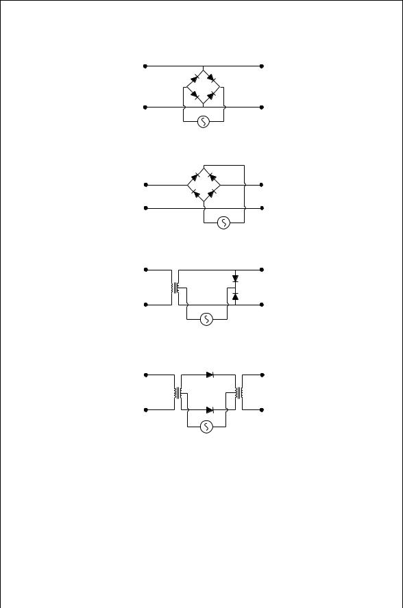
11.4SINGLE-BALANCED MIXERS
The single-balanced (or simply balanced) mixer has either two or four diodes as shown in the examples of Fig. 11.5. In all of these cases, when the LO voltage
f 1 
f1 
f1 
f1 
SINGLE-BALANCED MIXERS |
229 |
 f 0
f 0
+ |
– |
f p
(a )
 f 0
f 0
+ |
– |
f p
(b )
 f 0
f 0
+ |
– |
f p
(c )
 f 0
f 0
+ |
– |
f p
(d )
FIGURE 11.5 Four possible single-balanced mixers.
has a large positive value, all the diodes are shorted. When the LO voltage has a large negative value, all the diodes are open. In either case, the LO power cannot reach the IF load nor the RF load because of circuit symmetry. However, the incoming RF voltage sees alternately a path to the IF load and a blockage to the IF load. The block may either be an open circuit to the IF load or a short circuit to ground.

230 RF MIXERS
S(t )
1
0
T |
t |
FIGURE 11.6 Single-balanced mixer waveform.
As before, it is assumed that the LO voltage is much greater than the RF voltage, so Vp × V1. The LO voltage can be approximated as a square wave with period T D 1/fp that modulates the incoming RF signal (Fig. 11.6). A Fourier analysis of the square wave results in a switching function designated by S t :
|
1 |
|
1 |
sin n /2 |
|
|
S t D |
|
C |
|
|
cos nωpt |
11.16 |
2 |
nD1 |
n /2 |
||||
|
|
|
|
|
|
If the input RF signal is expressed as V1 cos ω1t, then the output voltage is this multiplied by the switching function:
V0 D V1 cos ω1t |
Ð S t |
1 |
n /2 |
cos nωpt |
11.17 |
||
D V1 cos ω1t |
|
2 |
C |
11.18 |
|||
|
|
1 |
|
sin n /2 |
|
|
|
|
|
|
|
|
|
|
|
nD1
Clearly, the RF input signal voltage will be present in the IF circuit. However, only the odd harmonics of the local oscillator voltage will effect the IF load. Thus the spurious voltages appearing in the IF circuit are
f1, fp C f1, 3fp š f1, 5fp š f1, . . .
and all even harmonics of fp are suppressed (or balanced out).
11.5DOUBLE-BALANCED MIXERS
The double-balanced mixer is capable of isolating both the RF input voltage and the LO voltage from the IF load. The slight additional cost of some extra diodes and a balun is usually outweighed by the improved intermodulation suppression, improved dynamic range, low conversion loss, and low noise. The two most widely used double balanced mixers for the RF and microwave band are the “ring” mixer and the “star” mixer depicted in Fig. 11.7. In the single-balanced mixer all the diodes were either turned on or turned off, depending on the instantaneous polarity of the local oscillator voltage. The distinguishing feature of the
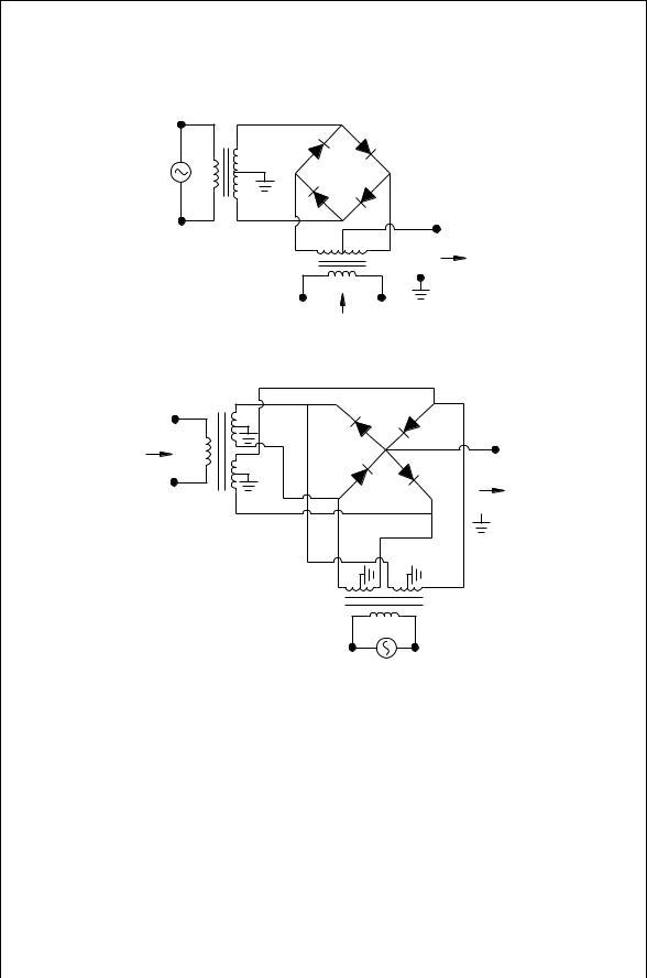
DOUBLE-BALANCED MIXERS |
231 |
|
A |
|
|
D 2 |
D 1 |
|
+ |
|
f p |
D |
C |
|
– |
D 3 |
|
D 4 |
B
f 0
f 1
(a )
D 1 |
D 2 |
f 1 |
|
D 3 |
D 4 |
f 0
– |
+ |
f p
(b )
FIGURE 11.7 Double-balanced mixers using (a) ring diode design and (b) diode star design.
double-balanced mixer is that half the diodes are on and half off at any given time. The diode pairs are switched on or off according to the local oscillator polarity. Thus the path from the signal port with frequency f1 to the intermediate frequency port, f0, reverses polarity at the rate of 1/fp.
In Fig 11.7a, when the LO is positive at the upper terminal, diodes D1 and D2 are shorted while diodes D3 and D4 are open. Current from the RF port