

Digital Design VHDL Laboratory
4.VHDL - Hardware Design Software Approach
pepe, 4/30/96
4. Digital Device Modeling
4.1 Introduction
Several VHDL concepts have been addressed in the previous lessons. VHDL topics covered in the previous lessons are various digital circuit modeling methodologies: structural, behavioral, and dataflow models. In addition to digital modeling, the text also covered the implementation of two types of state machines: Moore and Mealy state machines using the VHDL process statement. The Process statement is a unique feature in comparison to conventional imperative programming languages such as C, Pascal, FORTRAN, Ada, C++, etc. Due to the concurrent nature of VHDL programming, Process blocks execute/simulate in parallel. Statements inside of the process block, on the other hand, are executed sequentially. Parallel simulation is important because real world digital systems operate and behave in parallel. In the following lesson, this same concept of parallel executing process blocks will be addressed again. The emphasis here will be more towards the solving of real world application problems such as digital component modeling.
4.2 SRAM Memory
Memory plays an important role in the advancement of modern computers. When design a computing system, different types of memory are hierarchically structured into layers according to their data handling speed. The CPU is usually the fastest component and it is surrounded by various levels of memory. The various types of memory work in conjunction with the CPU: for example, on-chip and off-chip memory, memory chips surround the CPU on the motherboard, hard disk memory, and secondary memory device such as tape backups. To make computer efficient so the CPU will not be bogged down by the slower memory, different speeds of memory need to be used. Memory used by CPU are classified in general as SRAM (static RAM) and DRAM (dynamic RAM). SRAM memory runs faster than DRAM, and it interfaces directly with the CPU or the CPU on chip memory such as the L1 cache of the system. DRAM, on the other hand, is slower than SRAM by an order and requires more control circuitry, but has the advantages of smaller cell size and lower cost.
DRAM memory is denser than SRAM due to its circuit simplicity. Unlike SRAM which uses flip flops, DRAM stores information in capacitors, and information will only be kept until the charges in the capacitors leak out. As a consequence, more effort is needed to design DRAM “refresh circuitry” to preserve the stored DRAM information. Refreshing DRAM means re-charging the capacitors.
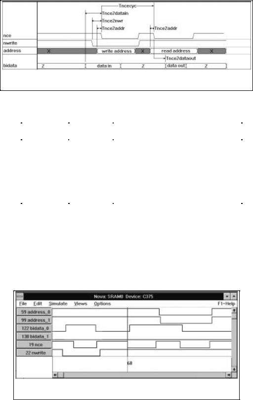
SRAM memory is much simpler to use than DRAM because it does not require a “refresh” operation. A generalized SRAM timing diagram is shown in Figure 4-1. SRAM is an asynchronous device. Read and write operations depend on the chip’s selecting signal nce shown in Figure 4-1. Typical timing parameters found in an SRAM data book include signal nce to various signal edges, which also shown in Figure 4-1.
The SRAM signals shown in Figure 4-1 are described in Table 4-1. The signal type entry in the table describes the signal direction attribute such as input, output or bidirectional. The line bidata is set to high impedence when it is not used. By doing so, bidata will not cause data line conflict.
Timing parameters for an SRAM are also illustrated in Figure 4-1. They are the minimum times starting from the signal nce to various signals and they are the same for both read and write operations. Signal nwrite indicates read or write operation. If the SRAM is in write mode, bidata will be the input for capturing data. Oppositely, if the SRAM is in read mode, bidata will be used to output data.
26 |
Copyright 1996, CERL / EE, V1.00 |
Digital Design VHDL Laboratory
4.VHDL - Hardware Design Software Approach
pepe, 4/30/96
Figure 4-1. SRAM Timing Diagram
|
Table 4-1. SRAM Signal Description |
||
|
|
|
|
Signal Name |
Signal Type |
Signal Description |
|
|
|
|
|
NCE |
IN |
Not chip select signal. |
|
NWrite |
IN |
Not chip write or chip read signal. |
|
Address |
IN |
Use for read and write address. |
|
Data |
IN/OUT |
Use for data input and data output. |
|
|
|
|
|
4.3 VHDL SRAM Memory Design
SRAM modeling can be implemented using the above timing information and previous VHDL lessons. A VHDL program that models a 2 bit by 4 word SRAM device is listed in Section 4.4. This program was compiled and simulated using the Cypress Warp tool. The simulation waveform is shown in Figure 4-2. From the figure, it can be seen that the data value 2 was written into the memory location 3 (bidata(1)=‘1’ and bidata(0)=‘0’) and read back afterwards.
Figure 4-2. SRAM Simulation Waveform
Several VHDL concepts were used in this program. The first is the use of the generic statement. The Generic statement is similar to constant declaration in programming languages except it is more useful
27 |
Copyright 1996, CERL / EE, V1.00 |
Digital Design VHDL Laboratory
4.VHDL - Hardware Design Software Approach
pepe, 4/30/96
due to the hardware design application. Notice that we have discussed a VHDL method for declaring constants in earlier lessons. Generic statement is different because it specifies where those constant are valid. In other words, the generic statement defines the scope of its constants. The Generic statement is to be used inside of an entity statement (see previous lessons), and the architecture body associated with this entity will be able to see and use these generic constants. It is a very powerful concept because it allows generalized hardware modeling. In the SRAM example, the size of the SRAM does not need to be fixed at 8 words deep and 2 bits per word. Different size SRAMs can be created by changing only the declaration inside of the generic statement.
The second concept is the use of the sub-program procedure statement. Although the component statement was introduced first, the procedure statement is the preferred construct due to its simplicity. The component structure is very much the same as the architecture structure. It uses an entity statement to specify input and output signals and an architecture body to define the relationship(s) of these signals. Declaration of a component is also needed in the main architecture body. As clear as the component concept may seem it, there are many hassles in creating and using component for simulation. Unless the component is useful or has already been created and put into a library, a procedure is the prefer choice.
Another reason why a procedure construct is preferred over a component construct is for ease of understanding VHDL code. In general, VHDL code for structure modeling is less likely to be comprehended than the corresponding behavior modeling which is naturally associated with procedure statement. The fact that behavior modeling is easier to grasp was shown in the previous lesson where a D flip-flop was represented in different VHDL models.
The third concept is the use of library routines. The use statement can be found between the entity statement and architecture statement. Since the Cypress VHDL compiler is mainly geared towards hardware synthesis, the behavior modeling aspect of Cypress VHDL compiler is weak because it doesn’t have good support for modeling a resistor. For example, in the SRAM modeling below, to multiplex bidirectional line, bidata, component tristate buffer, bufoe, from the Cypress library rtlpkg would have to be used.
4.4 SRAM VHDL Listing
---------------------------------------------------------------------
-- Entity statement
--
-- Specifies input, output and bidirectional signals -- Specifies
---------------------------------------------------------------------
entity sram0 is
generic(
address_width : integer := 2; -- column address width
address_size |
: integer := 4; |
|
word_width |
: integer := 2; -- word width |
|
zero_word : bit_vector := "00" -- To nullify a memory |
||
); |
|
|
port( |
|
|
address |
: in bit_vector (address_width-1 downto 0); |
|
nwrite |
: in bit; |
|
nce |
: in bit; |
|
bidata |
: inout x01z_vector (word_width-1 downto 0) |
|
); |
|
|
end sram0; |
|
|
use work.rtlpkg.all;
-- bufoe(x, oe, y, yfb): Three state buffer with feedback.
use work.int_math.all; -- See Cypress VHDL synthesis reference page 4-86 -- i2bv(i,w): converts integer i to w width binary
28 |
Copyright 1996, CERL / EE, V1.00 |
Digital Design VHDL Laboratory 4.VHDL - Hardware Design Software Approach pepe, 4/30/96
--signal.
--bv2i(a): inverse of function i2bv
---------------------------------------------------------------------
architecture sram0arch of sram0 is
type memory_elmt is array (address_size downto 0) of bit_vector (address_width downto 0);
---------------------------------------------------------------------
-- Read from the memory
---------------------------------------------------------------------
procedure ReadMemory ( nce, nwrite: in bit;
address: in bit_vector (address_width-1 downto 0); memory_word: in memory_elmt;
dataout: out bit_vector (word_width-1 downto 0)) is
variable i, w: integer; variable addressi: integer; begin
if (nce='0') and nce'event then if (nwrite='1') then
addressi := bv2i(address);
for i in 0 to address_size-1 loop if(i=addressi) then
for w in 0 to word_width-1 loop dataout(w) <= memory_word(i)(w);
end loop; end if;
end loop; end if;
end if;
end ReadMemory;
---------------------------------------------------------------------
-- Write to the memory
---------------------------------------------------------------------
procedure WriteMemory ( nce, NWrite: in bit;
Address: in bit_vector (address_width-1 downto 0); memory_word: out memory_elmt;
datain: in bit_vector (word_width-1 downto 0)) is variable i, w: integer;
variable addressi: integer; begin
if (nce='0') and nce'event then if (nwrite='0') then
addressi := bv2i(address);
for i in 0 to address_size-1 loop if(i=addressi) then
for w in 0 to word_width-1 loop memory_word(i)(w) <= datain(w);
end loop; end if;
end loop; end if;
end if;
end WriteMemory;
---------------------------------------------------------------------
-- Main program
---------------------------------------------------------------------
29 |
Copyright 1996, CERL / EE, V1.00 |