

ГОСУДАРСТВЕННОЕ ОБРАЗОВАТЕЛЬНОЕ УЧРЕЖДЕНИЕ
ВЫСШЕГО ПРОФЕССИОНАЛЬНОГО ОБРАЗОВАНИЯ
ВЯТСКИЙ ГОСУДАРСТВЕННЫЙ УНИВЕРСИТЕТ
ФАКУЛЬТЕТ ПРИКЛАДНОЙ МАТЕМАТИКИ И ТЕЛЕКОММУНИКАЦИЙ
Кафедра Радиоэлектронных Средств
Альбом схем для практических занятий
по дисциплине «Цифровые устройства и микропроцессоры»
Киров 2010
Содержание
ИК устройство дистанционного управления (Infra-red remote control)……………………………………………………………………..……………4
Система управления (An Evaluation System for Direct Interface of the MPX5100 Pressure Sensor with a Microprocessor)……...............……………..5
Interfacing LCD Modules to the Z8 MCU…………………………………………………………………………...……………...………………………..6
Устройство управления мощностью и напряжением (Universal Power and Voltage Control Using the Z8E001)……………………………………....7
Timekeeping Based on a 8-MHz Crystal (1 of 2)…………………………………………………………………...………………………..………………8
Timekeeping Based on a 60-Hz Power LineInterrupt…………………………………………………………………………………………..…………….9
Timekeeping Based on a 8-MHz Crystal (2 of 2)……………………………………………………………………...……………………………………10
Цифровое устройство нагревания воды ………………......………………………………………………………...………………………………...….11
Цифровое устройство нагревания воды - схема (Digital Instant Water Heater Schematic Diagram)…………………...…………..…………….11
Phase Control………………...………………………………………………………………………………………………………………………..12
Pulse Width Modulation (PWM)………………...……………………………………………………………………………………………………12
Zero-Crossing PWM………...………………………………………………………………………………………………………………………...12
Ноль-детектор (Zero-Crossing Detection)……...…………………………………………………………………………………………………....13
Температурный детектор (Temperature Detection)…………………………………………………………………………………………………13
User Interface…………...……………………………………………………………………………………………………………………………..14
Triac and Triac Driver…………………………………………………………………………………………………………………………………14
Schematic for a Dimmer Using the Z86E02 Microcontroller……………………………………………………………………………………………….15
Недорогой аналого-цифровой преобразователь (AVR400: Low Cost A/D Converter)………………………………………………………………....16
8-битный прецизионный АЦП (AVR401: 8-bit Precision A/D Converter)……………………………………………………………………………….17
Аналого-цифровые преобразователи……………….………………………. …………………………………………………………………………....18
Successive Approximation ADC……………………………………………………………………………………………………………………...18
Duty Cycle ADC……………………………………………………………………………………………………………………………………....19
Simple A/D for MCUs without built-in A/D converters…………………………………………………………………………………………………….20
Цифро-аналоговое преобразование (MAX529 DIGITAL-TO-ANALOG CONVERTER)……………………………………………………………...21
The R-2R DAC Network……………………………………………………………………………………………………………………………...21
Interfacing the HC05 MCU to a Multichannel Digital-to-Analog Converter Using the C68HC705C8A…………………………………………….22
Interfacing the HC05 MCU to a Multichannel Digital-to-Analog Converter Using the MC68HC705J1A………………………………………….23
Шаговый двигатель (Step Motor Step Sequence)………………………………………………………………………………………………………….24
DC MOTOR CONTROLLER USING THE ZILOG Z86E06 MCU………………………………………………………………………………………..25
DC Motor Controller Schematic……………………………………………………………………………………………………………………………..26
DC Motor Controller Schematic………………………….………………………………………………………………………………………………….27
PID Motor Control with the Z8PE003……………………………………………………………………………………………………………………....28
Limit Sensors………………………………………………………………………………………………………………………………………….29
H-Bridge……………………………………………………………………………………………………………………………………………….29
AVR242: 8-bit Microcontroller Multiplexing LED Drive and a 4 x 4 Keypad……………………………………………………………………………..30
Circuit Diagram for Keypad/Display Unit…………………………………………………………………………………………………………….30
Theory of Operation …………………………………………………………………………………………………………………………………..31
Keypad and LED connections (AVR240: 4 x 4 Keypad – Wake up on Keypress)…………………………………………………………………………32
ИК приемник дистанционного управления (AVR410: RC5 IR Remote Control Receiver)……………………………………………………………..33
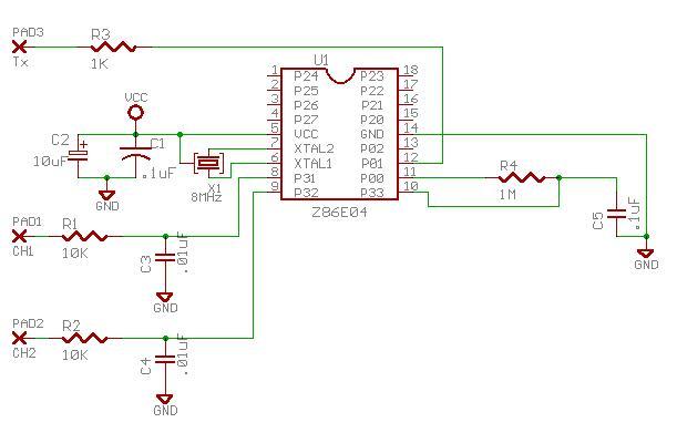
Схема формирования DTMF сигнала (DTMF Tone Generation Using the Z86E04 MCU)……………………………………………………………...34
Схема формирования DTMF сигнала (DTMF Tone Generation Using the Z86E04 MCU)……………………………………………………………...35
Схема телефонной трубки DTMF сигнала (Telephone Handset with DTMF using the 68HC05F4)………………………………………………….....36
Схема ……………………………………………………………………………………………………………………………………………………….37
Схема управления фазой (Power Phase Control Using Z8 Microcontrollers)…………………………………………………………………………….38
Канал широтно-импульсной модуляции (1 Channel DAC Using A PWM)…………………………………………………………………………….40
Схема мультиплексирования (Multiplexing Four 7-segments LEDs)……………………………………………………………………….…………....41
Схема мультиплексирования с клавиатурой 4 на 4 (Multiplexing Four 7-segments LEDs with a 4 x 4 Keypad)……………………………………...42
4х канальный вольтметр с клавиатурой и дисплеем (Four Channel Voltmeter with Display And Keypad)……………………………………………43
SRAM Block Schematic (STK 501)…………………………………………………………………………………………………………………….…..44
Схема………………………………………………………………………………………………………………………………………………………..45
Схема звукового термометра (Audible Thermometer Schematics)…………………………………………………………….…………………………46
Автоматический регулятор напряжения………………………………………………………………………………………………………………….47
Схема автоматического регулятора напряжения…………………………………………….…………………………………………………….47
Voltage Regulator Input……………………………………………………………………………………………………………………………….48
Voltage Regulator Output……………………………………………………………………………………………………………………………..48
Interfacing the MC68HC705J1A to 9356/9366 EEPROMs…………………………………………………………………………………………………49
Evaluation Board: Memories………………………………………………………………………………………………………………………………...50
Evaluation Board: Power, Crystal Oscillator, Clock Distribution and Power Supply Shutdown…………………………………………………………...51
Evaluation Board: Push Buttons, LEDs, Reset and Serial Interface………………………………………………………………………………………...52
Цифровой диктофон (Digital Sound Recorder with AVR and DataFlash: Microcontroller and Memory Circuit Diagram)……………………………...53
Цифровой диктофон (Digital Sound Recorder with AVR and DataFlash: Microphone and Speaker Circuit Diagram)………………………………….54
Макетно-отладочная плата. Принципиальная схема………………………………………………………………………………………………….....55
Макетно-отладочная плата. Принципиальная схема (продолжение)…………………………………………………………………………………...56
Контроллер-конструктор…………………………………………………………………………………………………………………………………..57
Управление LCD дисплеем (DIRECT DRIVE OF LCD DISPLAYS)…………………………………………………………………………………....58
Цепь управления (LCD Direct Drive Demo Circuit)………………………………………………………………………………………………...58
Multiple Backplanes…………………………………………………………………………………………………………………………………..59
PIC17C4X EXTERNAL RAM SCHEMATIC……………………………………………………………………………………………………………...60
Клавиатура (HC05 MCU Keypad Decoding Techniques Using the MC68HC705J1A)…………………………………………………………………...61

Рисунок 1 – ИК устройство дистанционного управления (Infra-red remote control)
After the initial set-up of the ports as inputs or outputs the remote control goes into STOP mode. It will remain in STOP mode as long as the device is not reset or a key is not pressed. When a key is pressed an interrupt request is generated. A short time delay makes sure that it is a true key press and not noise and also allows time for any switching effects on the inputs to pass prior to checking the inputs.
The keyboard is then read to find which key has been pressed and the code for the key is decoded into an instruction and transmitted to the television. If the key is held down the instruction is re-transmitted until the key is released. This is useful for the instructions which count through the television channels or adjust the volume, color or brightness controls. When the key is released a terminating instruction is sent to the receiver to inform it that the next message received is a separate instruction. This is useful in the case of a one time instruction like sending a channel number. In this example the receiver will tune to a channel only once; to tune to another channel the key must be released and a new instruction sequence received. After terminating the transmission the ports are reset ready for the next key press and the processor returns to the STOP mode.

Рисунок 2 – Система управления (DEVB-114 System Schematic: An Evaluation System for Direct Interface of the MPX5100 Pressure Sensor with a Microprocessor)
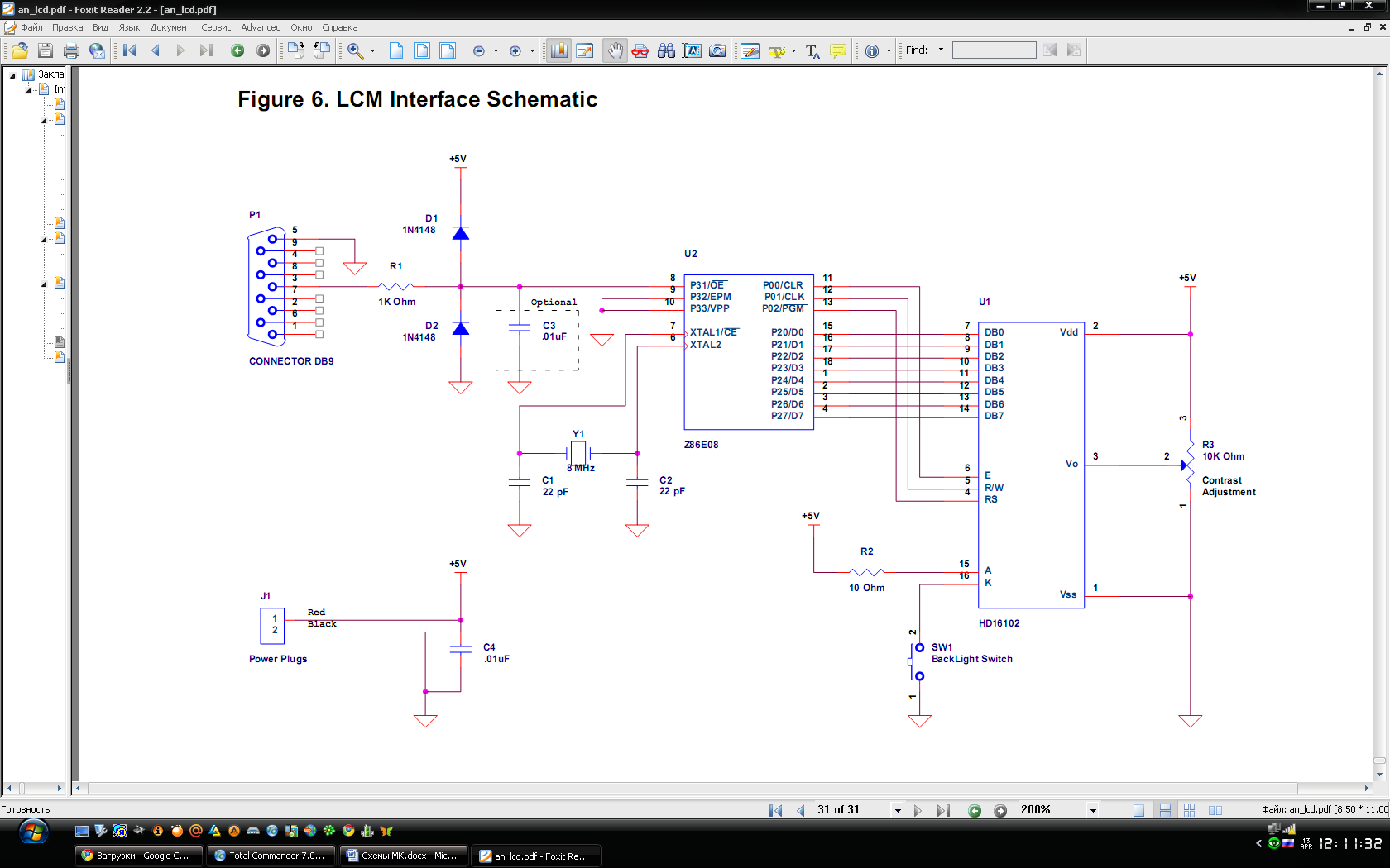
Рисунок 3 – Interfacing LCD Modules to the Z8 MCU
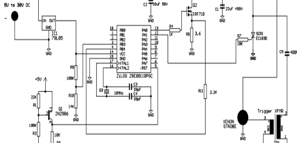
Рисунок 4 – Устройство управления мощностью и напряжением
(Universal Power and Voltage Control Using the Z8E001)
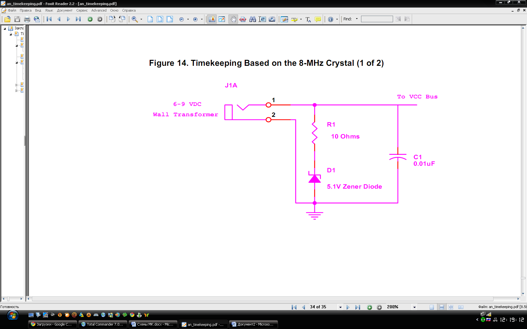
Рисунок 5 – Timekeeping Based on a 8-MHz Crystal (1 of 2)

Рисунок 6 – Timekeeping Based on a 60-Hz Power Line Interrupt
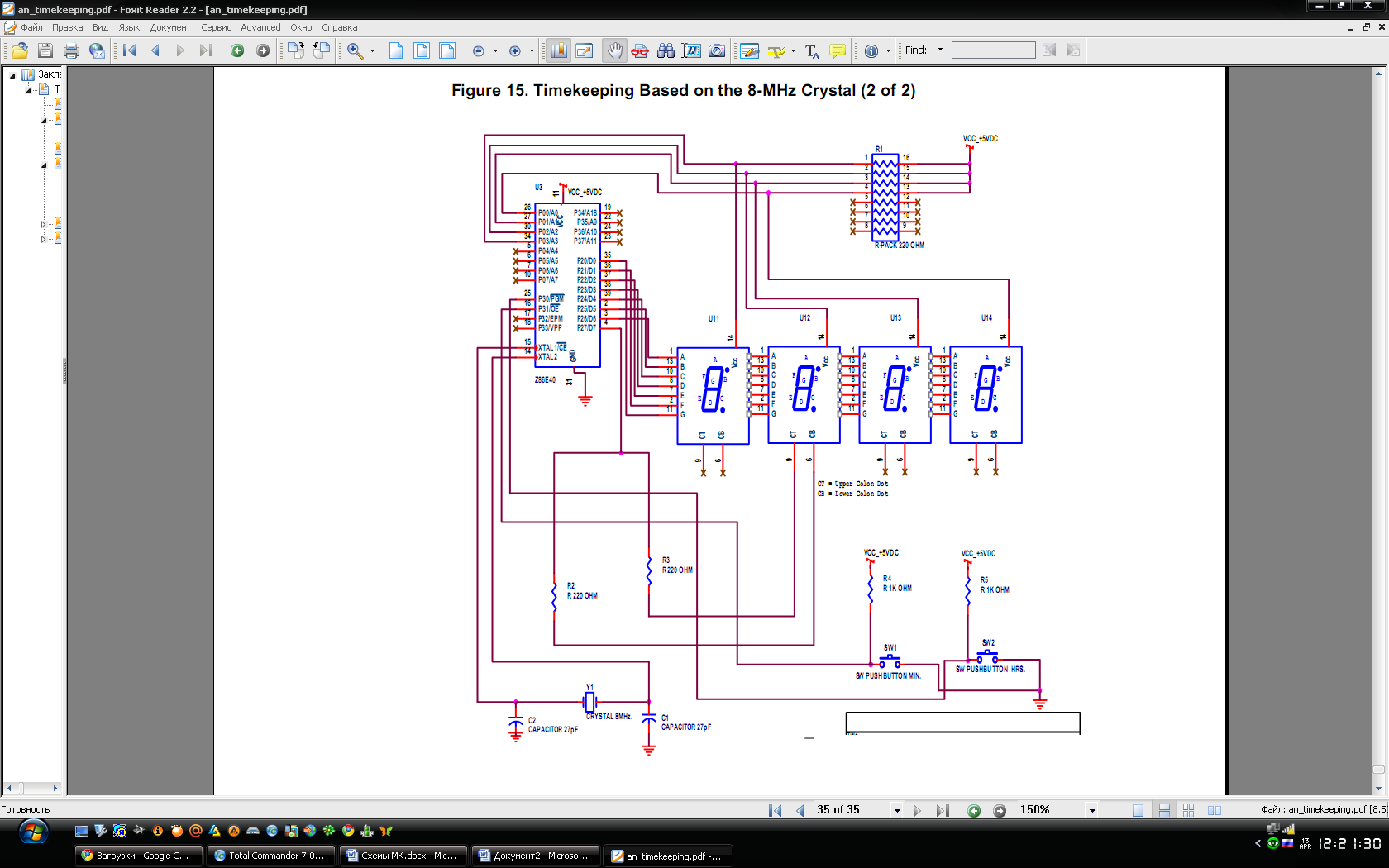
Рисунок 7 – Timekeeping Based on a 8-MHz Crystal (2 of 2)
Digital Instant Water Heater Schematic Diagram
Рисунок 8 – Цифровое устройство мгновенного нагревания воды
(Digital Instant Water Heater Schematic Diagram)
THEORY OF OPERATION
The conventional method of control is plain and simple: On/Off—full power or no power, and nothing in between. With the Z8® MCU, the power duty cycle can be controlled in a number of ways that vary the percentage of heater power output. The three common duty cycle control methods—Phase Control, Pulse-Width Modulation (PWM), and Zero-Crossing PWM—will each be discussed.
Phase Control
The
phase control method conducts power during a specific time period in
each half of the 50/60 Hz AC power cycle. Triacs are commonly used to
switch on/off the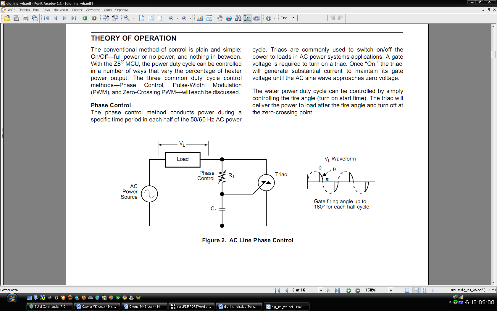
power to loads in AC power systems applications. A gate voltage is required to turn on a triac. Once “On,” the triac will generate substantial current to maintain its gate voltage until the AC sine wave approaches zero voltage. The water power duty cycle can be controlled by simply controlling the fire angle (turn on start time). The triac will deliver the power to load after the fire angle and turn off at the zero-crossing point.
Phase control can be easily implemented with a triac and a few passive components. However, the relationship between the firing angle and the power ratio is not linear. Getting an exact proportional output power is somewhat difficult. In addition, switching the triac on at the firing angle may induce high EMI. For a 220V AC line, switching at the peak voltage (311V) will generate a very high EMI noise, as an example. The European Community has imposed some restrictions on the EMI generation of an electrical appliance. Such EMI noise must be suppressed or reduced if the appliance is exported to Europe. As a complementary solution, a snubber or an EMI filter may be added to reduce the noise.
Pulse Width Modulation (PWM)
There
are always highs and lows in cyclical signals. By controlling the
width of the highs (Ta) and lows (Tb), the percentage of power (up to
full power) delivered to the load can be controlled. PWM is a
technique by which the power ratio is controlled by varying the duty
cycle of signal high time to total cycle time of the
cyclical signal. In this application, the cyclical signal is the AC power line.
One of the advantages of using PWM is its ease of implementation and subsequent lower cost; however, there are trade-offs to consider. Since the AC waveform is not linear, the power delivered during the peak voltage time will be higher than during the zero-crossing time, which means that power delivery is not linear. Also, the
frequency of the PWM signal will affect the smoothness of the power delivered. Generally, higher PWM frequency results in better smoothness. Finally, the On/Off switching of the PWM signal will induce EMI noise, which the designer must
minimize.
Zero-Crossing PWM
Since
our application uses the AC line at 50/60 Hz, this is the PWM
frequency of any PWM power control methodology. Because the power
delivery will be relatively unsmooth, the previously discussed PWM
technique can be combined with a zero-crossing switching technique to
form a “zero-crossing PWM” technique. With AC lines at 50/60 Hz,
the zero-crossing PWM technique combines the ease of implementing the
PWM methodology while minimizing the EMI noise induced and smoothing
the power delivery, which are some of the benefits of the
zero-crossing switching technique.
The AC power line is a sine wave with its peak voltage at π / 2 and minimum at 0 or π. If the power line frequency is 60 Hz, there will be 120 (60 Hz x 2) crossings. Power is turned on and off only at the zero-crossing point. Thus, the EMI will be minimized, and the power applied is smoothed as much as possible.
For example, if delivery of 25 percent of full power is desired, one AC cycle for every four AC cycles of appliance power will be turned on. This means that there are three “Off” AC cycles for every four AC cycles. Since the power potential of each cycle should be the same, there is a 25 percent power ratio. This method is also called “Cycle Skipping.”
Ноль-детектор (Zero-Crossing Detection)
A
Z8®
MCU controls the power level and senses the water temperature through
a thermistor. The Z8 MCU detects the zero-crossing points of the AC
power line and applies or removes AC power to the heating elements of
the water heater as needed. Refer to Figure 5 for the zero-crossing
detection circuitry.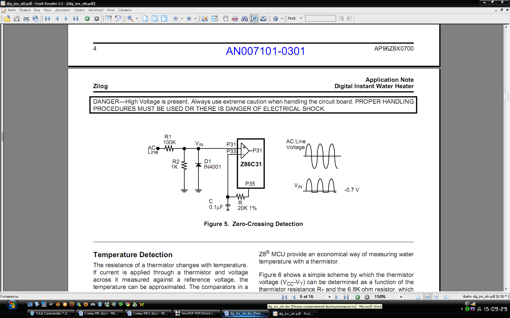
The AC power line is reduced by the potential divider resistors, R1 and R2. Since R2 is 1/100th of R1, the line voltage is divided by 100 times.
VIN = AC Line Voltage x R2 / (R1 + R2)
where VIN > -0.7V
Diode D1 is used to clamp the negative input voltage VIN to -0.7V minimum. Too much negative voltage may damage the MCU. The half AC waveform is connected to the positive input of the Z8 comparator (P31). Prior to zero-crossing detect, port pin P35 of the Z8 is cleared Low so that the reference input of the comparator
at P33 is zero volt. When the half AC waveform moving from positive to negative, the comparator output changes from one to zero. The edges of the comparator output signal corresponds to the zero-crossing points of the AC power line. By monitoring this signal, the zero-crossing point can be detected.
International Power Line Considerations Power line voltages vary from country to country and may be particularly unstable in some developing countries. For
example, a peak voltage may drop by as much as 10V when a 15A load is connected. In this case, the zero-crossing switch must be 10 Hz (or higher). The switching frequency can be doubled by switching at every half-cycle. (The power line has two zero crossings at an angle equal to 0 or π.)
Температурный детектор (Temperature Detection)
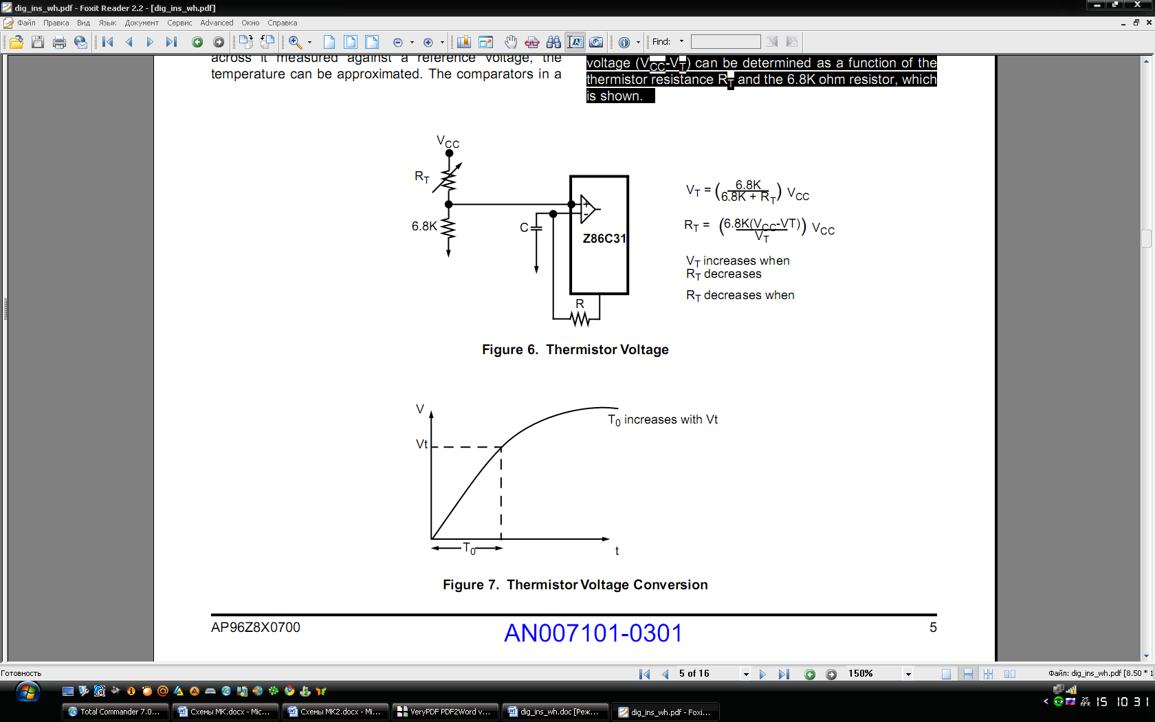

The resistance of a thermistor changes with temperature.
If current is applied through a thermistor and voltage across it measured against a reference voltage, the temperature can be approximated. The comparators in a Z8® MCU provide an economical way of measuring water temperature with a thermistor.
Figure 6 shows a simple scheme by which the thermistor voltage (VCC-VT) can be determined as a function of the thermistor resistance RT and the 6.8K ohm resistor, which is shown.
User Interface
There
are eight levels of selected water temperature. The power-up default
is at the preset level 4. The user can select warmer and cooler by
pressing the UP and DOWN buttons, respectively. The LEDs indicate the
selected level. 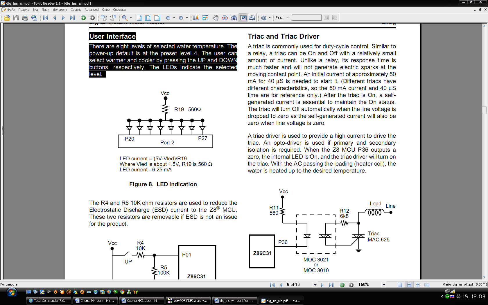
The R4 and R6 10K ohm resistors are used to reduce the Electrostatic Discharge (ESD) current to the Z8® MCU. These two resistors are removable if ESD is not an issue for the product.
Triac and Triac Driver
A
triac is commonly used for duty-cycle control. Similar to a relay, a
triac can be On and Off with a relatively small amount of current.
Unlike a relay, its response time is much faster and will not
generate electric sparks at the moving contact point. An initial
current of approximately 50 mA for 40 µS is needed to start it.
(Different triacs have different characteristics, so the 50 mA
current and 40 µS time are for reference only.) After the triac is
On, a self generated current is essential to maintain the On status.
The triac will turn Off automatically when the line voltage is
dropped to zero as the self-generated current will also be zero when
line voltage is zero.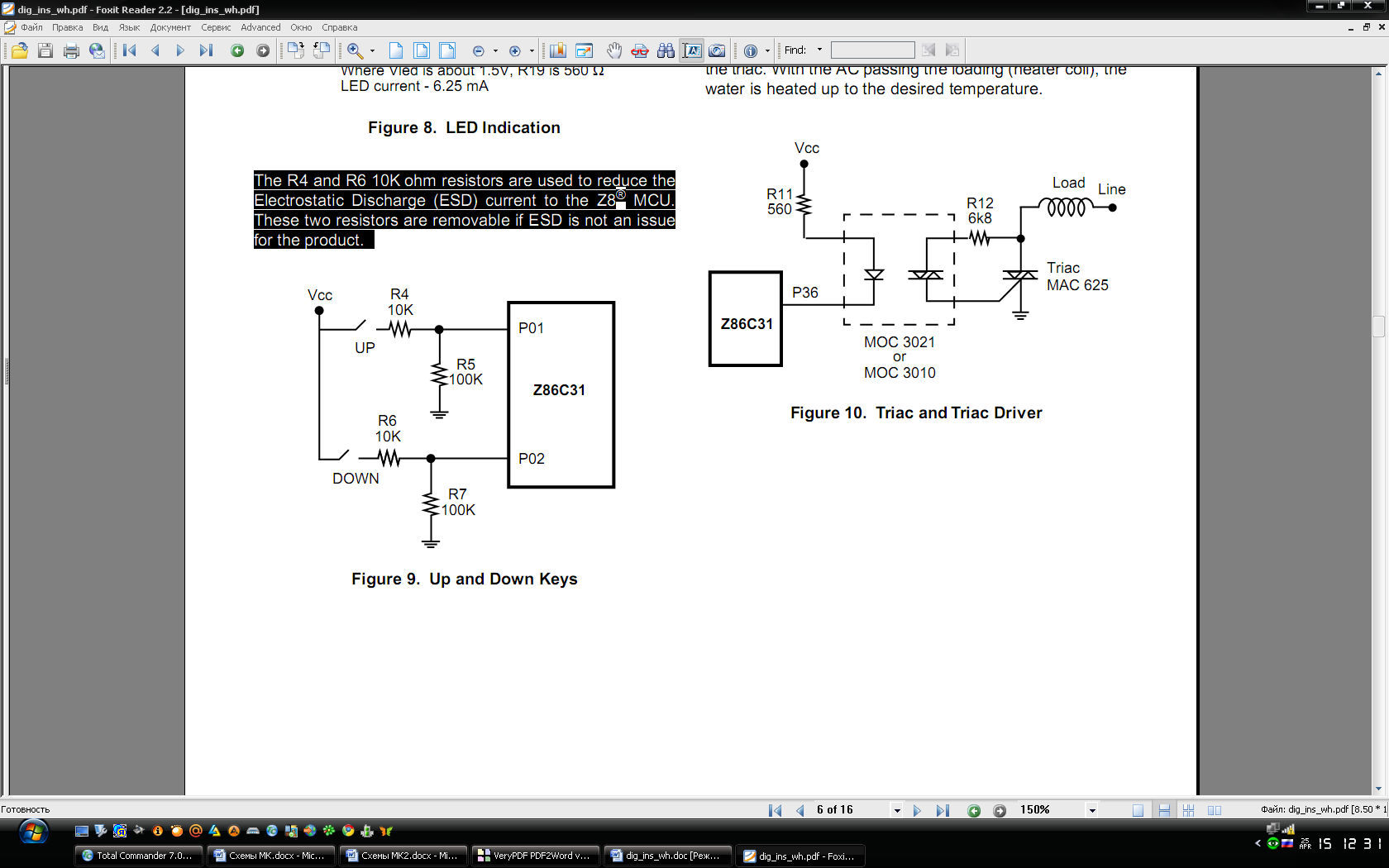
A triac driver is used to provide a high current to drive the triac. An opto-driver is used if primary and secondary isolation is required. When the Z8 MCU P36 outputs a zero, the internal LED is On, and the triac driver will turn on the triac. With the AC passing the loading (heater coil), the water is heated up to the desired temperature.
Рисунок 9 – Schematic for a Dimmer Using the Z86E02 Microcontroller
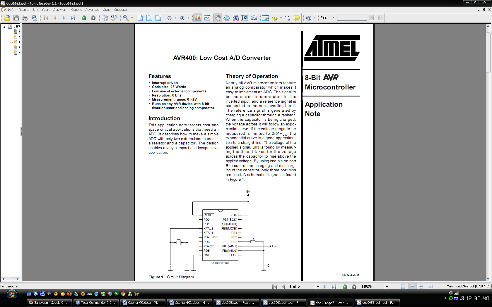
Рисунок 10 – Недорогой аналого-цифровой преобразователь (AVR400: Low Cost A/D Converter)
This application note targets cost and space critical applications that need an ADC. It describes how to make a simple ADC with only two external components, a resistor and a capacitor. The design enables a very compact and inexpensive application.
Theory of Operation
Nearly all AVR microcontrollers feature an analog comparator which makes it easy to implement an ADC. The signal to b e m e a s u r e d i s c o n n e c t e d t o t h e inverted input, and a reference signal is connected to the non-inverting input. The reference signal is generated by charging a capacitor through a resistor. When the capacitor is being charged, the voltage across it will follow an exponential curve. If the voltage range to be measured is limited to 2/5*VC C, the exponential curve is a good approximation to a straight line. The voltage of the applied signal, UIN is found by measuring the time it takes for the voltage across the capacitor to rise above the applied voltage. By using one pin on port B to control the charging and discharging of the capacitor, only three port pins are used.
This
application note describes how to perform a kind of dual slope A/D
conversion with an AVR microcontroller. The converter is very low
cost, requiring only six discrete components in addition to the AVR.
Five of the controller pins are used. This example is based on the
AT90S1200 device, but any AVR device with a comparator can be used.
Theory of Operation
The capacitor is charged with a constant current supplied by the transistor. The capacitor voltage will rise linearly. To discharge the capacitor, the AIN0-pin is set
to output with a ‘0’ applied. A reference voltage at VCC/2 is supplied by the resistor network Rref1 and Rref2. When the PB1 and PB2-pins are configured as
inputs, the reference is turned off, and the voltage level at the AIN1-pin will be the input voltage Vin. By setting the pins as outputs and applying a ‘0’ and a ‘1’,
the level at the AIN1-pin will be VCC/2 (if the resistors are of equal size). The input resistor Rin have to be at least 100 times higher than the reference resistors Rref1
and Rref2 to avoid measurement errors.
The algorithm used for the conversion is as follows:
1. Turn on the reference
2. Charge the capacitor until the reference voltage is
reached. Measure the time needed for this, Tref
3. Turn off the reference and discharge the capacitor
4. Charge the capacitor until the input voltage is
reached. Measure the time needed for this, Tin
Рисунок 11 – 8-битный прецизионный АЦП (AVR401: 8-bit Precision A/D Converter)
Аналого-цифровые преобразователи:
Successive Approximation ADC
For applications requiring fast conversion times, consider the successive approximation method. This method uses a Digital-to-Analog Converter (DAC) in its feedback loop. The DAC is comprised of an R2R ladder connected to port P2. When a binary value is output at Port 2, a DC voltage proportional to the binary value appears at pin 1 of the ladder network. The DAC completes a binary search on the input voltage. This search is achieved by first setting the most significant bit (MSB) of the DAC and testing the comparator output. If the comparator output is 0, the DAC output for this bit is set to 0. If the comparator output is 1, then the DAC output for this bit is set to 1. The bits from output port 2 are individually tested in ascending order, performing the same test. When all the bits are tested, the conversion is complete. The output from the R2R resistor network becomes the comparator's reference voltage. The analog voltage to be measured can be connected to either P31 or P32, the non-inverting inputs of the comparators.
To start the conversion, the MSB of P2 is set, resulting in a voltage of.5 Vcc at the VREF input of the comparator. If Vcc is 5V, then the voltage is 2.5V. The non inverting comparator input is tested. If High, then the analog voltage must be 2.5VР5.0V.
The next bit, P26, is set, and the input port is tested again. If LOW, then bit P26 is reset. The process continues until all bits of P2 are tested. The resultant value at
P2 is the digital representation of the analog input. With a crystal frequency of 8 MHz, the conversion time is approximately 110 µS. Even more resolution is avail-
able from 10- and 12-bit R2R networks. Of course, more resolution requires more port pins.
Рисунок 12 – АЦП последовательного приближения
Duty Cycle ADC
When speed is not important, a Duty Cycle Analog to Digital Converter is the perfect solution. This method works by measuring the time it takes a capacitor to
charge up above the input voltage and discharge below the input voltage.
Because the charge time is compared to the discharge time, component tolerances have no effect on accuracy, and the reading is linear. In addition to the comparators, only one port pin is required to control the RC network, leaving the balance of the I/O free. This example performs a two-channel, 11 bit conversion.
Because this method is based upon measuring time, the duty cycle ADC requires a stable time base. The stable time base is accomplished using only one interrupt
for the timer and ensuring that the softwareХs charge and discharge paths execute in the same amount of time.1
At each timer interrupt period, the capacitor is compared to the input voltage. If the capacitor is greater than the input voltage, than the capacitor is discharged
and the pass counter is decremented. If the capacitor is less than the input voltage, the capacitor is charged, the reading is incremented, and the pass counter is
decremented. When the pass counter reaches 0 the conversion is complete. For highest stability, the capacitor must be charged to the input voltage before
measurement begins. The easiest way to charge the capacitor to the input voltage is to perform two conversions and discard the first one. Also, the total conversion
time must be an even multiple of the line frequency (60Hz or 50Hz). This example is 2048 counts x 130 µ S = 266mS, approximately 16 cycles at 60 Hz, with
a 1M resistor and a.1 µ F capacitor. Total conversion time for both channels is 1.06S.
Рисунок 13 – АЦП циклического преобразования
Simple A/D for MCUs without built-in A/D converters:
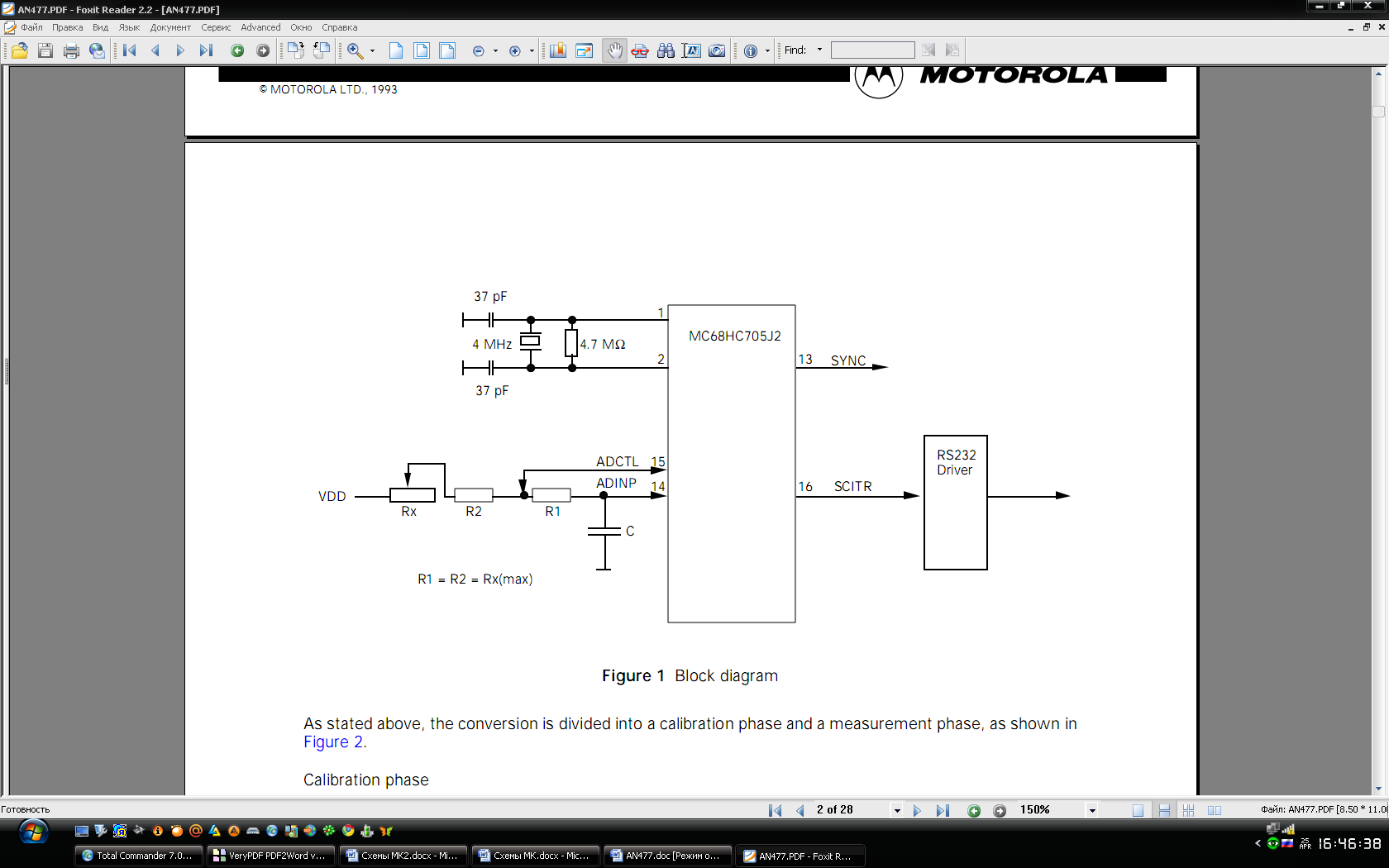
Block diagram:
–There are four I/Os used on the MCU.
–ADCTL is used both as an output and as an input.
–ADINP is always a high impedance input.
–Two outputs are used for debugging the system.
–SCITR is used to transmit the result serially.
–SYNC is a triggered signal for an external oscilloscope.
The conversion is divided into a calibration phase and a measurement phase.
Calibration phase
The calibration phase finds the R1*C time constant. This is done by first discharging the external capacitor C by pulling ADCTL low. Notice that the resistors Rx + R2 have no effect at all at this time.
Measurement
phase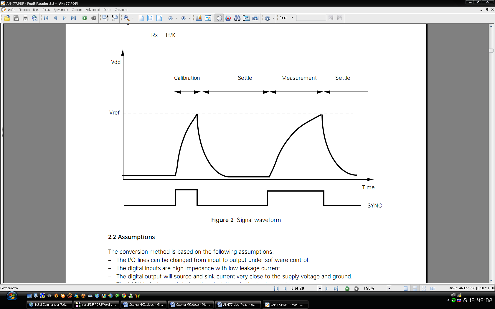
Then ADCTL is pulled high towards Vdd to charge the capacitor C. The time, Tc depending on R1*C, is measured to reach the threshold voltage, Vref, of ADINP. When the input signal passes the threshold level, the elapsed time is measured and stored. In other words the calibration time is:
Tc = R1 * C * ln(Vdd/(Vdd - Vref))
After the measurement, ADCTL is pulled low to discharge the capacitor C again.
The second measurement step makes the ADCTL go high impedance. The capacitor C immediately starts to charge. The time taken is given by the formula:
Tm = (R1 + R2 + Rx) * C * ln(Vdd/(Vdd - Vref))
The time to reach the threshold voltage is measured again. To make things simple we shall set R1 and R2 each equal to R.
Tm = (R + R + Rx ) * C * ln(Vref/(Vref - Vr)
The final result is calculated to get correct scaling.
Tf = Tm - 2 * Tc
Substitute with the values calculated before and replace the ln(Vref/(Vref - Vr) with K.
Tf = ((2 * R + Rx) - 2 * R) * K
Tf = Rx * K
Which gives the final result Rx = Tf/K
Цифро-аналоговое преобразование (MAX529 DIGITAL-TO-ANALOG CONVERTER)
The MAX529 is a monolithic device consisting of eight voltage output DACs. Two reference voltage inputs feed two sets of four DACs on the chip. A serial interface is used to communicate with the chip. The MAX528 operates from split supplies totaling up to 20 V, including +5 V and -15 V, +12 V and -5 V, and +15 V and -5 V, or a single supply up to 15 V. The MAX529 operates from -5 V supplies or from a single +5 V supply. This application note utilizes the MAX529 with a single +5 V supply. If low-power consumption is required, the part can be put in shutdown mode with its shutdown pin. During shutdown, the part uses less than 50 нA of current. The part can configure its buffer mode of the DAC output pins in three different ways:
1) An unbuffered mode connects the internal R-2R DAC network directly to the output pin.
2) A full-buffered mode inserts an op amp buffer between the R-2R network and the output pin, providing a +5 mA and -2 mA output drive.
3) A half-buffered mode is similar to the full-buffered mode but only provides up to +5 mA of output drive in a unipolar configuration.
If needed, the part can be serially daisy-chained to other 529s to increase the number of DACs in a system.
The R-2R DAC Network
The DAC inside the MAX529 is based on the R-2R resistor network. Most CMOS DACs are based on the R-2R current steering circuit. Figure 1 shows a simple 2-bit R-2R DAC. A reference voltage is applied to the VREF pin and the current, I, is binary divided throughout the array as shown. These currents are steered in discrete incremental amounts to the OUT1 and OUT2 nodes. The digital input to the DAC determines the position of the switches used to steer the current. A logic one causes the switch to steer the current to OUT1, while a logic zero causes the switch to steer the current to OUT2. OUT2 is at analog ground. The feedback configuration of the op amp forces OUT1 to be at virtual ground potential.
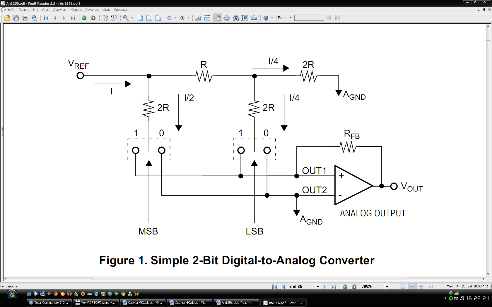
Рисунок 14 – Simple 2-Bit Digital-to-Analog Converter
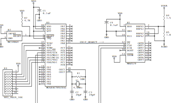
Рисунок 15 – Interfacing the HC05 MCU to a Multichannel Digital-to-Analog Converter Using the C68HC705C8A
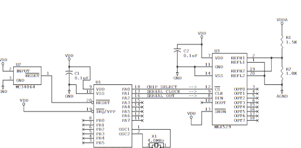
Рисунок 16 – Interfacing the HC05 MCU to a Multichannel Digital-to-Analog Converter Using the MC68HC705J1A