- •Suleyman demirel university
- •Contents
- •Preface
- •Preliminaries 1. Resistors’ colored codes.
- •Preliminaries 2. Measurements with digital multimeter.
- •Laboratory work # 1. Diode applications
- •Preparation to lab work.
- •Lab work performance.
- •Test questions
- •Laboratory work # 2. Realization of logic gates with transistors.
- •Preparation to lab work.
- •Lab work performance.
- •Test questions
- •A. On, on, on b. On, on, off c. Off,on, off
- •A. 1 p-n-junction b. 2 p-n-junctions c. 3 p-n-junctions
- •A. On, on, on b. On, on, off c. Off,on, off
- •A. On, on, on b. On, off, off c. Off,on, off
- •Laboratory work # 3. Logic gates.
- •Preparation to lab work.
- •Lab work performance.
- •Test questions
- •A. 1 b. 2 c. 3 d. 4 e. 5
- •A. Xor b. Xnor c. Nor d. Nand e. And
- •5. Nor is dual to a. Xor b. Xnor c. Nor d. Nand e. And
- •6. Or is complement to a. Xor b. Xnor c. Nor d. Nand e. And
- •A.1 b.2 c.3 d.4 e 5
- •Laboratory work # 4. Seven-segment displays
- •Preparation to lab work.
- •Lab work performance.
- •Test questions
- •A. Makes the several systems compatible b. Makes the two systems compatible c. Makes the two systems compatible even though each uses a different binary code
- •A. 0,0,1 b.1,0,1 c.1,1,0 d.0,1,0 e. 0,1,1
- •Laboratory work # 5. Four-bit binary parallel adder.
- •Preparation to lab work.
- •Lab work performance.
- •Test questions
- •A. Binary numbers b. Binary variables
- •A.Sequential; three
- •Test questions
- •A.Sequential; three b. Sequential; two c. Combinational; two d. Combinational; three e. Sequential or combinational; three
- •E. The sum of two bits and a previous carry, … the sum of two bits
- •Lab work performance.
- •Test questions
- •A. 1 b. 2 c. 3 d. 4 e. 5
- •A. Xor b. Xnor c. Nor d. Nand e. And
- •Laboratory work # 8. Decoder and demultiplexer.
- •Preparation to lab work.
- •Lab work performance.
- •Table #1
- •Table #2
- •Test questions
- •E. Converts binary information from n input lines to m output lines
- •Laboratory work # 9. Encoder.
- •Preparation to lab work.
- •What discrepancy may be for this scheme? lab work performance.
- •Test questions
- •Laboratory work # 10.
- •Test questions
- •A. Enable input of decoder b. Disable input of decoder
- •E. Disable input of multiplexer
- •Laboratory work # 11. D- flip-flop.
- •Preparation to lab work.
- •Lab work performance.
- •Test questions
- •A. Rs and clocked rs b.Rs or clocked rs c. D d. Jk e. T
- •A. Rs b. Clocked rs c. D d. Jk e. T
- •A. An expression to describe next state of the circuit
- •A. 1 b. 2 c. 3 d. 4 e. 5
- •Lab work performance.
- •Test questions
- •E. Decoder with enable can be used as multiplexer
- •A. 0000, 0001, 0010, 0011 b. 0000, 1000, 1100, 1110 c. 0000, 1000, 1001, 1010 d. 0000, 1000, 0001, 1001 e. 0000, 0001, 1000, 1001
- •A. 1, 0, 1
- •Test questions
- •A. A, c, d, e, f, g b. A, c, d, e, f c. A, b, c, f, g d. C, d, e, f, g e. A, b, c, d, e, f
- •A. To make a device active b. To provide the normal device’s operation
- •Laboratory work # 14. Bidirectional shift register.
- •Preparation to lab work.
- •Lab work performance.
- •Test questions
Lab work performance.
Demonstrate presence of your home preparation for lab work to your instructor.
Pass test of 10 questions.
Get a permission to begin the work.
Mount the scheme of experiment 11A on the breadboard and perform it. Fill in the table.
Make a conclusion about functionality of the scheme. Compare your results with theoretical ones.
Demonstrate your results to your instructor. If your results are correct you may dismount your scheme, if no – find the mistake.
Repeat steps 4-6 for experiment 11B.
Be ready to answer your instructor’s questions in process of work.
Complete your work, dismount your schemes, clean your working place.
Answer your instructor’s final questions, obtain your mark.
Ask your instructor’s permission to leave.
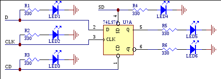
Experiment 11A.Realize the following circuit on a breadboard. Connecting D, CLK, CD, and SD inputs to either GND or VCC based on the following table, fill in the blanks. Write ON or OFF for LEDs.
|
INPUTS |
OUTPUTS | ||||||||
|
D |
CLK |
CD |
SD |
LED1 |
LED2 |
LED3 |
LED4 |
LED5 |
LED6 |
1 |
0V |
0V |
5V |
5V |
|
|
|
|
|
|
2 |
0V |
5V |
5V |
5V |
|
|
|
|
|
|
3 |
0V |
0V |
5V |
5V |
|
|
|
|
|
|
4 |
5V |
0V |
5V |
5V |
|
|
|
|
|
|
5 |
5V |
5V |
5V |
5V |
|
|
|
|
|
|
6 |
5V |
0V |
5V |
5V |
|
|
|
|
|
|
7 |
5V |
0V |
0V |
5V |
|
|
|
|
|
|
8 |
5V |
0V |
5V |
5V |
|
|
|
|
|
|
9 |
5V |
0V |
5V |
0V |
|
|
|
|
|
|
10 |
5V |
0V |
5V |
5V |
|
|
|
|
|
|
11 |
5V |
0V |
0V |
5V |
|
|
|
|
|
|
12 |
5V |
0V |
5V |
5V |
|
|
|
|
|
|
13 |
5V |
0V |
5V |
0V |
|
|
|
|
|
|
14 |
5V |
0V |
5V |
5V |
|
|
|
|
|
|
15 |
0V |
0V |
5V |
5V |
|
|
|
|
|
|
16 |
0V |
0V |
0V |
5V |
|
|
|
|
|
|
17 |
0V |
0V |
5V |
5V |
|
|
|
|
|
|
18 |
0V |
0V |
5V |
0V |
|
|
|
|
|
|
19 |
0V |
0V |
5V |
5V |
|
|
|
|
|
|
20 |
0V |
5V |
5V |
5V |
|
|
|
|
|
|
21 |
0V |
0V |
5V |
5V |
|
|
|
|
|
|
22 |
0V |
0V |
0V |
5V |
|
|
|
|
|
|
23 * |
0V |
0V |
0V |
0V |
|
|
|
|
|
|
24 |
0V |
0V |
5V |
0V |
|
|
|
|
|
|
25 |
0V |
0V |
5V |
5V |
|
|
|
|
|
|
* be careful at that stage!
Based on the above truth table, it is a ………. type flip flop, with ……… is the input, …….. is the clock input, ……….. is the output, and ……… is the inverting output. SD is ………………………… and CD is …………………………
Experiment 11B.Mount the D-Flip-Flop circuit implemented with NAND gates on the breadboard. Compare results with the results obtained in experiment 11A.
Conclusion.