

ivchenko_bookreg
.pdf1 Kingdom of Nanostructures
Let him lose himself in wonders as amazing in their littleness as the others in their vastness.
Of these two Infinites of science, that of greatness is the most palpable...
But the infinitely little is the least obvious. Philosophers have much oftener claimed to have reached it, and it is here they have all stumbled.
Blaise Pascal: Pens´ees
Due to continued progress in nanotechnology, novel semiconductor structures are fabricated with subnanometer accuracy and precisely controlled the electronic and optical properties. This progress in nanoscale engineering, as well as an improved understanding of the physical phenomena at the nanometer scale, have contributed to the rapid development of low-dimensional physics of semiconductors. At present a certain system of concepts and terms is accepted in this field of solid state physics. First of all the following vocabulary of semiconductor nanoscience has been developed: Quantum Well (QW), QW structure, Single and Double QWs, Multiple QWs (MQWs), Superlattice (SL), Quantum Wire (QWR) and Quantum Well Wire (QWW), Quantum Dot (QD) or Quantum Box, Nanocrystal, Antidot, Quantum Microcavity, Photonic Crystals, Porous Semiconductor Material, Nanoclaster, Nanotube and, particularly, Carbon Nanotube, Type-I and Type-II Heterostructures, δ-Doped Structure, Strained Structure, Nanocontacts, ... The nomenclature of novel quantum states in nanostructures includes Quantum-Confined states of free charge carriers and excitons, Subbands and Minibands, Folded Acoustic Phonons, Confined Optical Phonons, Interface Phonon Modes, LowDimensional Magnetic Polarons, Composite Fermions, Edge States in the Quantum Hall E ect.
In this chapter we briefly discuss the typical nanostructures progressing in the order from Two-Dimensional (2D) to One-Dimensional (1D) and Zero-Dimensional (0D) systems. Size-quantization and modification of energy spectra of quasi-particles in nanostructures are considered in Chap. 2.
1.1 Multilayered Heterostructures: Quantum Wells and
Superlattices
The Quantum Well (QW) is a system in which the electron motion is restricted in one direction, thus producing the quantum confinement. In other words, the energy spectrum in one of the quantum numbers changes from continuous to discrete. For quantum confinement to be observable, the size

21 Kingdom of Nanostructures
of a well must be less than the electron mean-free-pass length. This requirement imposes constraints on the well’s geometric size, the sample quality and temperature.
The simplest 2D object on which the quantum confinement e ects were revealed and studied are silicon-bases Metal-Oxide-Semiconductor (MOS) structures with a triangular confining potential formed at the semiconductor boundary and single GaAs/Al1−xGaxAs heterojunctions where a confining potential is created in the GaAs layer at the heterostructure boundary. It is on these structures that the quantum Hall e ect, an unexpected and remarkable phenomenon occurring in a 2D electron gas, was discovered. However, in the following we will mainly concentrate on multilayered structures without built-in electric fields.
Fig. 1.1. Band diagrams of single type-I (a) and type-II (b) heterojunctions.
We start with a single heterojunction between two compositional semiconductors A and B, as illustrated in Fig. 1.1. In the figure, the higher and lower broken lines show the coordinate dependence of the conduction-band bottom and the valence-band top in the direction of the principal axis z, or the growth direction. One or both constituent materials can be alloy semiconductors, for instance, ternary solid solution Al1−xGaxAs or Cd1−xMnxTe. Di erent examples of A/B heteropairs are GaAs/Al1−xGaxAs, In1−xAlxAs/Ga1−y Aly As, InAs/AlSb, Ga1−xInxAs/InP, CdTe/Cd1−xMnxTe, Zn1−xCdxSe/ZnSy Se1−x, ZnSe/BeTe, ZnSe/GaAs, Si1−xGex/Si and so forth, where the subscripts x, y or 1 − x, 1 − y show the fraction of atoms of particular kind at sites of the crystal lattice or one of its sublattice. By definition, in type-I heteropairs the band gap of one material, the material A in Fig. 1.1a, lies inside the band gap of another material. In this case the potential wells for the electrons and holes

1.1 Multilayered Heterostructures: Quantum Wells and Superlattices |
3 |
are located in the same layer, e.g., GaAs layer in the GaAs/Al1−xGaxAs heterostructures with x < 0.4. The potential-barrier heights coincide with the conductionand valence-band o sets, ∆Ec = EcB −EcA and ∆Ev = EvA −EvB. The sum ∆Ec + ∆Ev equals the di erence ∆Eg between the band gaps EgB and EgA. In the technologically important GaAs/Al1−xGaxAs heterosystem, the ratio ∆Ec/∆Eg is about 0.6.
In type-II structures the conduction-band bottom is lower in one layer, the layer A in Fig. 1.1b, whereas the valence-band top is higher in the neighboring layer B. It is clear that in type-II multilayered heterostructures, like GaAs/Al1−xGaxAs with x > 0.4, InAs/AlSb or ZnSe/BeTe, the electrons and holes are confined within di erent layers. A special case of type-II behavior is a heterostructure, e.g. InAs/GaSb, where the top EvA of the valence band in layer A lies above the bottom of the conduction band, EcB. Heteropairs with one of the materials being a gapless semiconductor (e.g. HgTe/CdTe) are referred to as a type-III heterostructure.
Fig. 1.2. Band diagrams of single QW (a) and single barrier (b) structures. Ve,h are, respectively, the conductionand valence-band o sets, or barrier heights.
A type-I double heterojunction B/A/B represents a single QW structure if EgA < EgB, see Fig. 1.2a, and a single barrier structure if EgA > EgB, Fig. 1.2b. In the former case the inner layer A forms a potential well size-quantizing the electron and hole states. In the latter, the layer A prevents free carriers from free exchange between the leftand right-hand-side layers B. It is clear

41 Kingdom of Nanostructures
that a type-II double heterojunction is a single QW structure for one sort of carriers, say, for electrons, and, at the same time, a single barrier structure for charge carriers of the opposite sign. The structure with the confining potential shown in Fig. 1.2a is a rectangular QW. By varying properly the composition along the growth direction, one can produce wells of another shape, e.g., parabolic, triangular, etc.
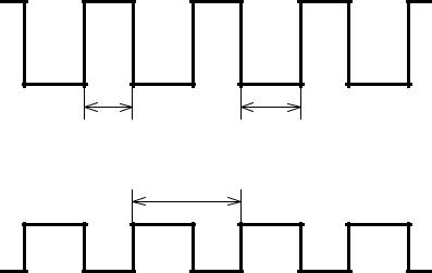
Fig. 1.3. Band diagrams of double-barrier (a), triple-barrier (b) and double-QW (c) structures.
A natural extension of a single barrier structure is double- and triplebarrier structures illustrated in Figs. 1.3a and b. Similarly, the concept of the single QW can be extended to double QWs (Fig. 1.3c), triple QWs and structures containing a set of QWs (Fig. 1.4). A periodic system of QWs separated by barriers thick enough to make them impenetrable for charge carriers is called Multiple Quantum Wells (MQWs). As regards electronic properties of MQWs, each of QWs is isolated from others. However, the electronic excitations within individual QWs can be coupled by electromagnetic fields and the presence of many wells a ects noticeably optical characteristics of the structure. As the barriers get thinner, carrier tunnelling from one well to another becomes possible and, as a result, the quantum-confined states, or subband states, of an isolated well transform into miniband states. In that way the concept of MQWs transmutes into the concept of SuperLattice (SL). The miniband formation becomes actual when the SL period d = a + b is smaller than the mean-free-path length, or phase-coherence length, in the growth direction. This length can be dependent on the sort of carriers, particularly, due to di erence in the electron and hole e ective masses. Therefore, the same periodic QW structure can be a SL for electrons which have, as a rule, a smaller e ective mass and MQWs, or thick-barrier SL, for heavy holes. In this case the holes can also travel along the growth axis. However this motion
1.1 Multilayered Heterostructures: Quantum Wells and Superlattices |
5 |
has no a coherent character and can be described as a series of incoherent tunnelling hoppings between neighboring wells. As the barrier thickness continues to decrease, the minibands corresponding to particular subbands of a single QW begin to overlap. Such UltraThin SLs, e.g. (GaAs)n(AlAs)m, with the layer thicknesses being usually not in excess of three-four monomolecular layers (n, m = 2 ÷ 4), behave as an anisotropic bulk crystal whose properties, however, di er substantially from those of the original materials. Strictly speaking, the definition of a SL presupposes that the layer thicknesses a and b must exceed the crystal-lattice constant in order to allow one to apply the e ective mass approximation, or the envelope function method, for the description of electronic states. Nevertheless, it is instructive to include the ultrathin SLs, and even the compound (GaAs)1(AlAs)1 = GaAlAs2, into the field of vision in the low-dimensional physics as the limiting case of a SL with d → 0.
b |
a |
d
Fig. 1.4. Band diagram of a periodic structure consisting of the alternating well and barrier layers with the thicknesses a and b, respectively. It is called a multiple QW structure, if the barriers are thick, or a SL, if the barriers are thin.
Similarly to the above classification of heterostructures by the band alignment schemes, each SL belongs to one of three types, labelled type-I, II and III. The SLs consisting of alternating layers of di erent materials are called compositional. QWs and SLs were initially produced by choosing heteropairs with practically equal lattice constants a0, for example, GaAs/AlGaAs pair. The structures with the lattice mismatch ∆a0/a0 less or equal ≤ 0.01 are called unstrained, or lattice matched. Progress in growth technology has made it possible to obtain dislocation-free structures out of materials with notice-
61 Kingdom of Nanostructures
ably di erent lattice constant. In this case at least one of the layers, A or B, must be thin enough, and the crystal lattices match because of internal stresses which result in a compression of one of the adjacent layers and a tension of the other. The QWs and SLs with ∆a0/a0 ≥ 0.01 are called strained. In spin SLs one or both layers A and B contain magnetic impurities or ions, e.g., CdTe/CdMnTe. Besides the compositional SLs produced by varying the composition, one can prepare SLs by modulation doping with a donor and an acceptor impurity (modulation doped SLs). The examples are a n-GaAs/p- GaAs SL and a nipi SL formed by n- and p-doped layers with intrinsic layers i between them. By varying smoothly the composition, one can produce SLs with wells and barriers of arbitrary shape, for instance, saw-tooth lattices with triangular wells. Keldysh [1.1] was the first to propose a superlattice by deforming a crystal with a strong standing acoustic wave. Esaki and Tsu [1.2] suggested instead composition modulation or selective doping, a method successfully implemented. In 1971, Kazarinov and Suris formulated a pioneer idea of a novel semiconductor laser, making use of stimulated light emission in a semiconductor SL by electrons making transitions between two levels of the di erent wells and emitting photons. This photon-assisted tunnelling mechanism, which does not involve the valence-band holes, had remained a purely theoretical prediction for over 20 years. The successful work on far infrared lasers based on this idea and called the quantum cascade lasers was reported in [1.6].
In addition to periodic structures, it is possible to produce and study aperiodic SLs. The Fibonacci SL may serve as an example of such a structure. It contains two basic elements (or blocks) A and B. In the first realization [1.3]
|
˚ |
˚ |
the basic elements were composed nominally of (17 A AlAs)-(42 A GaAs) |
||
˚ |
˚ |
|
and (17 A |
AlAs)-(20 A GaAs), respectively. The Fibonacci sequence, Sj , of |
|
order j is obtained from the blocks A and B following the rules: S0 = A, S1 = AB, Sj = Sj−1Sj−2 (j ≥ 2). In particular, S2 = ABA, S3 = ABAAB...
The sequence Sj (j ≥ 2) comprises Gj elements A and Gj−1 elements B, Gj being the jth Fibonacci number given by the values G0 = G1 = 1 and the
recurrent relation G |
j |
= G |
j−1 |
+G |
j−2 |
. Particularly, G |
2 |
= 2, G |
= 3, G = 5, ... |
||
|
|
|
|
|
3√ |
|
4 |
||||
As j increases the ratio Gj /Gj−1 converges toward τ = (1 + |
5)/2. The Fi- |
||||||||||
bonacci SLs are, in some sense, an intermediate case between periodic and disordered 1D potentials. They reveal interesting and striking features in the band structure, wave-function localization and optical transitions [1.4].
1.2 Quantum Wires and Nanotubes
Technologically, the step from the 2D QW structures fabricated by thin-film growth down to one dimension is complicated. While several growth techniques are well suited to produce planar multilayer systems, the fabrication of Quantum Wire (QWR) structures in which charge carriers are quantum

1.2 Quantum Wires and Nanotubes |
7 |
confined in two dimensions is a very challenging task. The first methods suggested and attempted allowed to grow 1D structures called Quantum Well Wires (QWWs), i.e., 2D carrier-confinement structures in which carriers can move freely only in one direction. For example, a QWW can be prepared as a result of the lateral structuring of a QW by means of lithographic processing with etching and regrowth. The dimensionality of a 2D QW can be also reduced by using a special electrode configuration or strain lateral gradients to constrict the free carriers to a quasi-1D channel. Patterned interdi usion and implantation locally alter the band gap of a QW also allowing fabrication of a QWW.
Fig. 1.5. (a) Typical cross-sectional TEM image of a V-shaped GaAs/AlGaAs QWR. (b) Schematic illustration of the QW crescent and the upper interface. Grey and dark stripes symbolize interface roughness. From [1.9].
Among methods suggested and attempted to fabricate QWRs di erent from QWWs, the growth on vicinal substrate has been suggested and attempted [1.7]. Another method that is utilized for growing uniform single and multiple semiconductor QWRs relies on deposition of thin layers on V- grooved substrates [1.8]. Figures 1.5a and 1.5b show a typical Transmission Electron Microscope (TEM) image of a V-shaped GaAs/AlGaAs QWR and a demonstrative illustration of the interface geometry [1.9]. The V-grooved substrates with a V-groove period of 2 or 4 µm were prepared by photolithography and wet chemical etching on (001)±0.1%-oriented GaAs substrate along
¯
the [110] direction. Before epitaxial growth, the substrates were cleaned ultrasonically by organic solvent and additionally etched. This allowed to reduce greatly the interface roughness on the initial V-grooved substrates and improve uniformity of the grown QWRs. Epitaxial growth was performed with MetalOrganic Vapor Phase Epitaxy (MOVPE) system. The AlGaAs cladding layer grows to form a very sharp corner between two {111} crystal planes. The GaAs quantum well grows faster along the [001] direction, which results
81 Kingdom of Nanostructures
in the formation of a crescent-shaped QW at the bottom of the groove. The GaAs to AlGaAs upper interface is composed of three clear crystalline facets, one (001) and two (311)A. The lateral tapering in the thickness of the QW crescent provides lateral variation in the e ective band gap due to the increase in the carrier confinement energy with decreasing QW thickness. This lateral variation results in a 2D confining potential of the V-grooved QWR. By repeating the growth process it is possible to obtain vertically stacked multiple GaAs/AlGaAs QWR structures [1.10].
An e ective Molecular Beam Epitaxy (MBE) technique called Cleaved Edge Overgrowth makes possible fabrication of a T -shaped intersection of two QWs, or a T -shaped QWR [1.11,1.12]. In this method, after conventional growth of a single QW, double QWs or MQWs on a [001] oriented substrate, the structure is further cleaved along the [110] direction and overgrown on the cleaved edge by a perpendicular QW and a barrier layer. Figure 1.6 shows a cross-sectional transmission electron micrograph of the multiple T - shaped GaAs/AlGaAs QWRs (a) and a schematic cross-sectional view of the QWR laser structure (b). One can see from Fig. 1.6a that T -shaped QW intersections are indeed located at the cleavage plane. The quantum mechanical bound states of an electron at two intersecting QWs are discussed in Sect. 2.2.2.
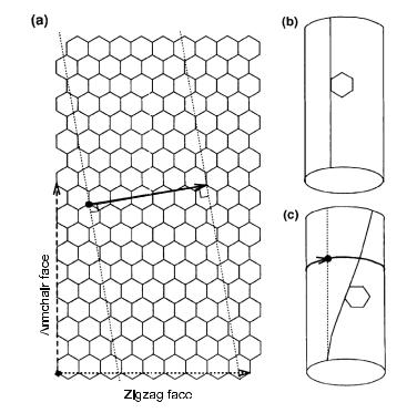
Carbon is a rare element that possesses the ability to form a wide variety of network-like sp2 structures which can be looked upon as graphitic sheets curved in order to eliminate the dangling bonds. In particular, these networklike nanostructures include such nanoclusters as the fullerene molecule C60, single carbon cages other than C60, e.g., C70, and multishell fullerenes, as well as carbon nanotubes, or carbon fibers. It is established that an arc discharge can produce either fullerenes or nanotubes by changing the conditions of the discharge. In fact, with the discovery by Iijima [1.14] of carbon nanotube structures, a new class of materials with the 1D dimensionality, or QWRs, has been introduced. The nanotubes are made of coaxial graphite cylinders, see Figs 1.7b and 1.7a. Each cylinder can be visualized as the conformal mapping of a 2D honeycomb graphene lattice (Fig. 1.7a) onto its surface. Multiwalled, or multiwall, carbon nanotubes consist of several concentric cylinders of the hexagonal network arranged around each other. In what follows we concentrate on singlewalled, or single-shell, nanotubes consisting of one cylinder.
A singlewalled nanotube is specified by a 2D hexagonal lattice vector L called the chiral, or circumferential, vector. Such a nanotube is obtained by rolling a graphite sheet along the vector L and joining one end of the vector to the other end as shown in Fig. 1.7. Thus, the length of circumference is L = |L| and the radius of the cylinder is L/(2π). Each perfect carbon nanotube is translationally periodic along the tube principal axis with the period being dependent on the vector L. Particular nanotubes with the chiral vector being parallel or perpendicular to one of elementary hexagon sides, see dashed and dotted lines in Fig. 1.7a, are called armchair and zigzag nan-

1.3 Nanocrystals and Quantum Dot Structures |
9 |
||||||||
|
|
|
|
|
|
|
|
|
|
|
|
|
|
|
|
|
|
|
|
|
|
|
|
|
|
|
|
|
|
|
|
|
|
|
|
|
|
|
|
|
|
|
|
|
|
|
|
|
|
|
|
|
|
|
|
|
|
|
|
|
|
|
|
|
|
|
|
|
|
3µ


µ
 µ
µ


Fig. 1.6. (a) Cross-sectional bright-field transmission electron micrograph of a
¯
multiple T-shaped QWR structure taken in the [110] zone axis, i.e., with the electron beam aligned along the wire axis. Dark areas correspond to GaAs or GaAs-rich regions. (b) Schematic cross-section of the QWR laser structure. The MQW layer consists of 22 GaAs QWs separated by Al0.35Ga0.65As barriers as illustrated in the magnified part of the QWR region. From [1.13].
otubes, respectively. Other nanotubes are characterized by a screw rotation symmetry and called the chiral nanotubes.
Introducing topological defects, pentagons, heptagons and octagons, in the carbon hexagonal network, one can connect di erent single-walled nanotubes to form three-terminal nanotube heterojunctions, in particular, T and Y junctions, which can be useful in nanoscale electronic devices, see [1.16, 1.17] and references therein.
1.3 Nanocrystals and Quantum Dot Structures
Quantum Dots (QDs) are nanoinclusions of one material inside another material. A semiconductor QD provides charge carrier confinement in all three directions and behaves as an artificial atom. Initially, QDs as well as QWRs were fabricated by the lateral structuring of QWs, including lithographic patterning and etching, selective intermixing by implantation and interdiffusion, strain-induced lateral confinement, growth on patterned substrates, see details in the book [1.18]. Here we discuss in more detail two other
10 1 Kingdom of Nanostructures
Fig. 1.7. (a) The hexagonal 2D lattice of a graphite monoatomic layer (graphene). A carbon nanotube is uniquely determined by the chiral vector, L, shown by a solid arrow. Long-dashed and dotted vectors give rise to armchair and zigzag nanotubes. (b) A graphene sheet rolled up to form a zigzag nanotube. (c) A rolled graphene sheet representing chiral carbon nanotubes. From [1.15].
fabrication techniques for QDs, namely, Stranski-Krastanow growth of selforganized QDs [1.19–1.21] and formation of nanocrystals in semiconductor doped glasses [1.23].
There are three possible modes of heteroepitaxial growth, namely, Frankvan der Merve, Volmer-Weber and Stranski-Krastanow, representing respectively ‘layer-by-layer’, ‘island’ and ‘layer-by-layer plus island’ modes. The particular growth mode for a given heteropair depends on the interface energies and on the lattice mismatch. Experimental results and theoretical analysis [1.22] show that, in the lattice-mismatched InAs/GaAs system, the Stranski-Krastanow mode is realized. At the initial stage, the growth occurs layer by layer to form a wetting layer with the microscopic thickness of one or two monomolecular layers. With increasing InAs deposition threedimensional (3D) coherent strained islands appear which can have the shape of a pyramid with a square base as illustrated in Fig. 1.8. For a dilute system