


Power Amplifier; Concepts and Challenges |
17 |
4.Classification of Power Amplifiers
Power amplifiers have been traditionally categorized under many classes: A, B, C, AB, D, E, F, etc [32]. Power amplifier classes can be categorized either as bias point dependent, such as classes A, B, AB, and C, or depending on the passive elements in the output matching network that shape the drain voltage and current, provided that the transistor in this case operates as a switch. In the next subsections, the details of each operating class are discussed.
4.1Class A, B, AB, and C PAs
The primary distinction between these power amplifier classes is the fraction of the RF cycle for which the transistor conducts. For class A PAs, the transistor is conducting for the entire RF cycle, whereas for class B PAs it is ON for half the RF cycle, and for less than half the RF cycle for class C. Class A, AB, and B amplifiers may be used as linear PAs, whereas class C are more nonlinear in nature [33]. Figure 2.4 illustrates the schematic and current waveforms for the above-mentioned classes of operation. While the third-order intercept point (IP3), adjacent channel power ratio (ACPR), 1 dB compression point, and harmonics are various measures of Linearity of PAs, drain efficiency and power added efficiency (PAE) of the PA are used to indicate the current drawn from the supply. The PAE is defined as

18 RF CMOS POWER AMPLIFIERS:THEORY,DESIGN AND IMPLEMENTATION
where  is the RF output power,
  is the RF input power, and
  is the total dc power drawn from the supply.
The efficiency and output power for a power amplifier operating in class A,
AB, B, or C, are given by [30];
where |
is the supply voltage, |
is the conduction angle of the drain cur- |
rent,  is the pinch-off voltage (knee voltage), and
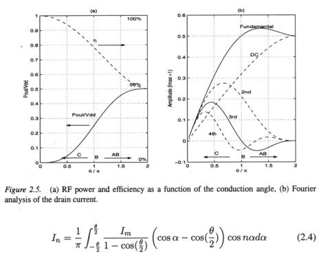
  is the maximum drain current in the input transistor. Equations (2.2) and (2.3) are plotted in Figure 2.5(a). From this figure, it is evident that the increase in efficiency, obtained by reducing the conduction angle is achieved at the expense of the reduced output power from the power amplifier. In deep sub-micron technologies, the low output power of a reduced conduction angle is a major drawback. In order to achieve the required output power, the load resistance has to be lowered to impractical values considering the values of the parasitic resistances.
As the conduction angle of the drain current decreases, the harmonic content of the current signal increases. The magnitude of the nth harmonic of the output
drain current is given by [30];
Power Amplifier; Concepts and Challenges |
19 |
By examining Figure 2.5(b), it is clear that the dc component decreases monotonically as the conduction angle is reduced. In class B, the fundamental component is the same as in class A while the dc component is reduced by  For conduction angles below
  corresponding to class C operation, the dc component continues to drop, but the fundamental component of the current signal also starts to drop below its class A level. This results in high efficiency, and lower power utilization factor (PUF). The odd harmonics can be seen to pass through zero at the class B point, For class AB mode, the third harmonic is not negligible. Still, class AB represents a compromise between linearity, PUF, and efficiency.
4.2Class E
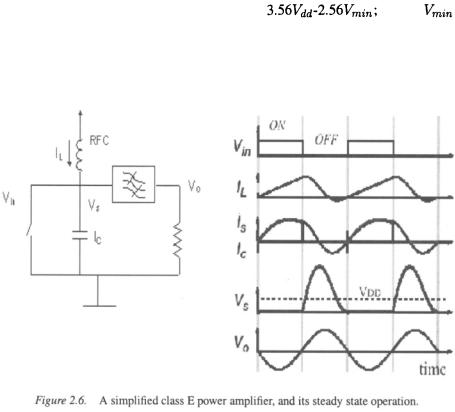
Figure 2.6 shows a conceptual picture of a class E power amplifier [34], [35].
In operation, the input signal  toggles the switch periodically with approximately 50% duty cycle. When the switch is ON, a linearly increasing current is built up through the inductor. At the moment the switch is turned off, this current is steered into the capacitor, causing the voltage across the switch
  to rise. The tuned network is designed such that in steady state,
  returns to zero with a zero slope, immediately before the switch is turned on. The band pass filter then selectively passes the fundamental component of
 to the load, creating a sinusoidal output that is synchronized in phase and frequency with
20 RF CMOS POWER AMPLIFIERS:THEORY,DESIGN AND IMPLEMENTATION
the input. In practical applications,  may be phase or frequency modulated, in which case the information embedded in the modulation is also passed to the output with power amplification [13].
By comparing  and
and  in Figure 2.6, it can be observed that the switch voltage and current are never simultaneously nonzero. Since the instantaneous power dissipation of the switch is the product of these two quantities, the switch is ideally lossless, and all the power from the dc supply is delivered to the radio frequency output. In addition, the capacitor is designed to be fully discharged before the switch is turned ON.
In high-speed operation, the switch transition time can become a signifi- cant fraction of a signal period. During these transitions, the switch voltage and current may be simultaneously nonzero, causing potential power loss in typical switching-mode amplifiers. For proper class E operation, this loss is alleviated at the turn on transistors by a zero switch current resulting from the simultaneously zero  and
and  On the other hand, turnoff transition loss is reduced by delaying the switch voltage rise until the switch is turned off. These properties have made class E-PAs attractive for high efficiency operations.
One of the features of class E amplifiers is the large peak voltage that the
switch sustains in the off state, approximately |
Where |
is the minimum voltage across the transistor. |
Operating at class E requires |
either high transistor breakdown voltage, or operating at  less than the specified value for a given technology. The equations describing the operation of class E will be discussed in Chapter 3.