

03.Combinational circuits
.pdfChapter 3 − Combinational Circuits Page 1 of 26
Table of Content
Table of Content ........................................................................................................................................................... |
1 |
||
3 Combinational Circuits ......................................................................................................................................... |
2 |
||
3.1 |
Analysis of Combinational Circuits .............................................................................................................. |
2 |
|
3.1.1 |
With a Truth Table................................................................................................................................ |
2 |
|
3.1.2 |
With a Boolean Function....................................................................................................................... |
4 |
|
3.2 |
Synthesis of Combinational Circuits............................................................................................................. |
5 |
|
3.3 |
Technology Mapping .................................................................................................................................... |
6 |
|
3.4 |
Minimization of Combinational Circuits ...................................................................................................... |
9 |
|
3.4.1 |
Karnaugh (K) Maps............................................................................................................................... |
9 |
|
3.4.2 |
Don’t-cares.......................................................................................................................................... |
13 |
|
3.4.3 |
* Quine-McCluskey (Tabulation) Method .......................................................................................... |
14 |
|
3.5 |
* Timing Hazards and Glitches................................................................................................................... |
15 |
|
3.6 |
7-Segment Decoder Example...................................................................................................................... |
16 |
|
3.7 |
VHDL Code for Combinational Circuits .................................................................................................... |
19 |
|
3.7.1 |
Structural BCD to 7-Segment Decoder ............................................................................................... |
19 |
|
3.7.2 |
Dataflow BCD to 7-Segment Decoder................................................................................................ |
22 |
|
3.7.3 |
Behavioral BCD to 7-Segment Decoder ............................................................................................. |
22 |
|
3.8 |
Summary Checklist ..................................................................................................................................... |
23 |
|
3.9 |
Exercises ..................................................................................................................................................... |
24 |
|
Index |
....................................................................................................................................................................... |
|
26 |
Microprocessor Design – Principles and Practices with VHDL |
Last updated 7/17/2003 5:56 PM |

Chapter 3 − Combinational Circuits
3 Combinational Circuits
Digital circuits, regardless of whether they are part of the control unit or the datapath, are classified
as either one of two types: combinational or sequential. Combinational circuits are the class of digital circuits where the outputs of the circuit are dependent only on the current inputs. They do not remember the history of past inputs and, therefore, do
not require any memory elements. Sequential circuits on the other hand are circuits in which their outputs are dependent on not only the current inputs but also
on past inputs. Because of their dependency on past inputs, sequential circuits must contain memory elements in order to remember the past input values.
A “large” digital circuit, however, may contain both
combinational circuits and sequential circuits. However, regardless of whether it is a combinational circuit or a sequential circuit, it is nevertheless a digital circuit, and so they use the same basic building blocks – the AND, OR and NOT gates. What makes them different is in the way the gates are connected.
The car security system example from Section 2.9 is an example of a combinational circuit. In the example, the siren is turned on when the master switch is on and someone opens the door. If you close the door then the siren will turn off immediately. With this setup, the output, which is the siren, is dependent only on the inputs, which are the master and door switches. For the security system to be more useful, the siren should remain on even after closing the door after it is first triggered. In order to add this new feature to the security system, we need to modify it so that the output is not only dependent on the master and door switches, but also dependent on whether the door has previously been opened or not. A memory element is needed in order to remember whether the door was previously opened or not, and this results in a sequential circuit. In this chapter, we will look at the design of combinational circuits. We will leave the design of sequential circuits for a later chapter.
In addition to being able to design a functionally correct circuit, we would also like to be able to optimize the circuit in terms of size, speed, and power consumption. Usually, reducing the circuit size will also increase the speed and reduce the power usage. In this chapter, we will only look at reducing the circuit size. Optimizing the circuit for speed and power usage is beyond the scope of this book.
3.1Analysis of Combinational Circuits
Very often we are given a digital logic circuit and we would like to know the operation of the circuit. The analysis of combinational circuits is the process in which we are given a combinational circuit and we want to derive a precise description of the operation of the circuit. In general, a combinational circuit can be described precisely either with a truth table or with a Boolean function.
3.1.1 With a Truth Table
For example, given the combinational circuit of Figure 1, we want to derive the truth table that describes the circuit. We create the truth table by first listing all the inputs found in the circuit, one input per column, followed by all the outputs found in the circuit. Hence, we start with a table with four columns; three columns (x, y, z) for the inputs and one column (f) for the output as shown below
x |
y |
z |
f |
|
|
|
|
Microprocessor Design – Principles and Practices with VHDL |
Last updated 7/17/2003 5:56 PM |

Chapter 3 − Combinational Circuits |
Page 3 of 26 |
x |
y |
z |
|
|
f |
Figure 1. Sample combinational circuit.
The next step is to enumerate all possible combinations of 0’s and 1’s for all the input variables. In general, for a circuit with n inputs there are 2n combinations from 0 to 2n – 1. Continuing on with the example, the table below list the eight combinations for the three variables in order.
x |
y |
z |
f |
0 |
0 |
0 |
|
0 |
0 |
1 |
|
0 |
1 |
0 |
|
0 |
1 |
1 |
|
1 |
0 |
0 |
|
1 |
0 |
1 |
|
1 |
1 |
0 |
|
1 |
1 |
1 |
|
Now, for each row in the table, that is, for each combination of input values, determine what the output value is. This is done by substituting the values for the input variables and tracing through the circuit to the output. For example, using xyz = 000, the outputs for all AND gates are 0, and ORing all the zeros gives a zero, therefore, f = 0. This is shown in the annotated circuit below.
x |
y |
z |
|
0 |
0 |
0 |
|
|
1 |
1 |
|
|
|
0 |
|
|
|
0 |
|
|
|
0 |
f |
|
|
0 |
|
|
|
0 |
|
For xyz = 001, the output for the top AND gate gives a 1, and 1 OR with anything gives a 1, therefore, f = 1 as shown in the annotated circuit below.
Microprocessor Design – Principles and Practices with VHDL |
Last updated 7/17/2003 5:56 PM |
Chapter 3 − Combinational Circuits |
Page 4 of 26 |
x |
y |
z |
|
0 |
0 |
1 |
|
|
1 |
1 |
|
|
|
1 |
|
|
|
0 |
|
|
|
1 |
f |
|
|
0 |
|
|
|
0 |
|
Continuing in this fashion for all input combinations, we can complete the final truth table for the circuit as shown below
x |
y |
z |
f |
0 |
0 |
0 |
0 |
0 |
0 |
1 |
1 |
0 |
1 |
0 |
0 |
0 |
1 |
1 |
1 |
1 |
0 |
0 |
0 |
1 |
0 |
1 |
1 |
1 |
1 |
0 |
0 |
1 |
1 |
1 |
1 |
3.1.2 With a Boolean Function
To derive a Boolean function that describes a combinational circuit, we simply write down the Boolean logical expressions at the output of each gate instead of substituting actual values of 0’s and 1’s for the inputs as we trace through the circuit from the primary input to the primary output. Using the sample combinational circuit of Figure 1, we note that the logical expression for the output of the top AND gate is x'y'z. The logical expressions for the following AND gates are respectively x'yz, xy'z, and xyz. Finally, the outputs from these AND gates are all ORed together. Hence, we get the final expression
f = x'y'z + x'yz + xy'z + xyz
To help keep tract of the expressions at the output of each logic gate, we can annotate the outputs of each logic gate with the resulting logical expression. If we substitute all possible combinations of values for the variables, we should obtain the same truth table as above.
Example 3.1
As another example, consider the combinational circuit below,
x |
y |
z |
|
|
f |
Starting from the primary inputs x, y, and z, we annotate the outputs of each logic gate with the resulting logical expression. Hence, we obtain the annotated circuit below
Microprocessor Design – Principles and Practices with VHDL |
Last updated 7/17/2003 5:56 PM |

Chapter 3 − Combinational Circuits |
Page 5 of 26 |
x |
y |
z |
|
|
|
|
|
|
|
y' |
xy' |
|
|
|
|
|
|
|
|
|
|
|
|
|
|
|
y |
z |
xy' + (y |
z) |
z)) |
|
|
x' |
|
f = x' (xy' + (y |
|||
|
|
|
|
|
|
|
The output of the circuit is the final function f = x' (xy' + (y z)). |
♦ |
3.2Synthesis of Combinational Circuits
Synthesis of combinational circuits is just the reverse procedure of the analysis of combinational circuits. In synthesis, we start with a description of the operation of the circuit. From this description, we derive either the truth table or the Boolean logical function that precisely describes the operation of the circuit. Once we have either the truth table or the logical function, we can easily translate that into a circuit diagram.
For example, let us construct a 3-bit comparator circuit that outputs a 1 if the number is greater than or equal to 5, and 0 otherwise. In other words, a circuit that outputs a 0 if the input is a number between 0 and 4, and outputs a 1 if the input is a number between 5 and 7. Since we are working with decimal numbers in the range 0 to 7, we can use three input bits (x2, x1, and x0) to represent the number. From the description, we obtain the following truth table
x2 |
x1 |
x0 |
f |
0 |
0 |
0 |
0 |
0 |
0 |
1 |
0 |
0 |
1 |
0 |
0 |
0 |
1 |
1 |
0 |
1 |
0 |
0 |
0 |
1 |
0 |
1 |
1 |
1 |
1 |
0 |
1 |
1 |
1 |
1 |
1 |
In constructing the circuit, we are only interested in when the output is a 1, i.e. when the function is a 1. Thus, we need only consider the rows where the output function f = 1. From the above truth table, we see that there are three rows where f = 1 which give the three AND terms x2x1'x0, x2x1x0', and x2x1x0. Notice that the variables in the AND terms are such that it is inverted if its value is a 0, and not inverted if its value is a 1. In the case of the first AND term, we want f = 1 when x2 = 1 and x1 = 0 and x0 = 1, and this is satisfied in the expression x2x1'x0. Finally, we want f = 1 when either one of these three AND terms is equal to 1. So we ORed the three AND terms together giving us our final expression
f = x2x1'x0 + x2x1x0' + x2x1x0
In drawing the schematic diagram, we simply convert the AND operators to AND gates and OR operators to OR gates. The equation is in the sum-of-product format, meaning that it is summing (ORing) the product (AND) terms. A sum-of-product equation translates to a two level circuit with the first level being made up of AND gates and the second level made up of OR gates. Each of the three AND terms contain three variables, so we use a 3-input AND gate for each of the three AND terms. The three AND terms are ORed together, so we use a 3-input OR gate to connect the output of the three AND gates. For each inverted variable, we need an inverter. The schematic diagram derived from the above equation is shown below
Microprocessor Design – Principles and Practices with VHDL |
Last updated 7/17/2003 5:56 PM |
Chapter 3 − Combinational Circuits |
Page 6 of 26 |
x2 |
x1 |
x0 |
|
|
f |
3.3Technology Mapping
To reduce implementation cost and turnaround time, designers often make use of off-the-shelve semi-custom gate arrays. Many gate arrays are ICs that have only NAND gates or NOR gates built in them, but their input and output connections are not yet connected. To use these gate arrays, a designer simply has to specify where to make these connections between the gates. The problem in using these gate arrays to implement our circuit is that we need to convert all AND gates, OR gates, and inverters in our circuit to use only NAND gates or NOR gates depending on what is available in the gate array. More over, these NAND and NOR gates usually have the same number of fixed inputs; usually 3-input.
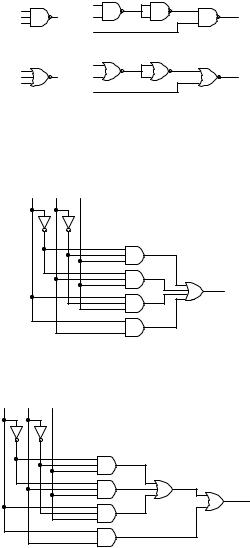
The conversion of any given circuit to use only NAND or NOR gates is possible by observing the following equalities as obtained from the Boolean algebra theorems:
Rule 1: x' ' = x
Rule 2: xy = ((xy)')'
Rule 3: x + y = ((x + y)')' = (x' y' )'
Rule 4: xy = ((xy)')' = (x' + y')'
Rule 5: x + y = ((x + y)')'
Rule 1 simply says that a double inverter can be eliminated altogether. Rule 2 applies Rule 1 to the AND operator. The resulting expression, however, gives us a NAND gate followed by an inverter. Rule 3 changes an OR gate to use two inverters and a NAND gate by first applying the double inverter rule and then De Morgan’s Theorem. Similarly, Rule 4 converts an AND gate to use two inverters and a NOR gate, and Rule 5 converts an OR gate to a NOR gate followed by an inverter.
Rules 2 and 3 are used if we want to convert an AND OR circuit to use only NAND gates, whereas, rules 4 and 5 are used if we want to use only NOR gates.
In a circuit diagram, these rules translate to the following equivalent circuits
Rule 1: 

 =
=
Rule 2: |
= |
Rule 3: |
= |
Rule 4: |
= |
Rule 5: |
= |
Microprocessor Design – Principles and Practices with VHDL |
Last updated 7/17/2003 5:56 PM |

Chapter 3 − Combinational Circuits |
Page 7 of 26 |
Finally, to replace inverters with either the NAND gate or the NOR gate, we note that by simply connecting all the inputs of either the NAND or the NOR gate together, the resulting operation of the gate is like the inverter. Take the 2- input NAND gate for example, we connect the two inputs together so that there is only one input and one output as follows
Since x and y will always have the same value, we can simplify the NAND gate truth table by eliminating the two rows where x ≠ y as shown in the truth table below. The two resulting columns for x and y are now identical and therefore, can be combined into just one column for the one input. As a result, we get a truth table that is exactly the same as that for the inverter.
|
NAND |
|
|
Inverter |
||||
|
|
|
|
|
|
|
|
|
x |
|
|
y |
|
f |
|
|
|
0 |
|
0 |
|
1 |
|
x |
f |
|
0 |
|
|
1 |
|
1 |
|
0 |
1 |
1 |
|
|
0 |
|
1 |
|
1 |
0 |
1 |
|
|
1 |
|
0 |
|
|
|
Similarly, we can get the same functional result by connecting together the two inputs for a NOR gate as shown below.
|
NOR |
|
|
Inverter |
|
x |
y |
f |
|
x |
f |
0 |
0 |
1 |
|
||
0 |
1 |
0 |
|
0 |
1 |
1 |
0 |
0 |
|
1 |
0 |
1 |
1 |
0 |
|
|
|
The inverter function can also be obtained from a 2-input NAND gate by connecting one of its inputs to 1. As shown in the truth table below, by connecting the input x to 1, the first two rows of the table where x = 0 can never occur. This way, with only the last two rows, whatever the second input y is, the output f is always the inverted value of y.
NAND |
Inverter |
x |
y |
f |
|
x |
f |
0 |
0 |
1 |
|
||
0 |
1 |
1 |
|
0 |
1 |
1 |
0 |
1 |
|
1 |
0 |
1 |
1 |
0 |
|
|
|
Another thing that we might want is to get the functionality of a 2-input NAND or NOR gate from a 3-input NAND or NOR gate respectively. The following circuit shows how you can get a 2-input NAND/NOR gate from a 3-input NAND/NOR gate respectively. You may want to check with a truth table that they are indeed equivalent.
2-input NAND gate |
2-input NOR gate |
Microprocessor Design – Principles and Practices with VHDL |
Last updated 7/17/2003 5:56 PM |
Chapter 3 − Combinational Circuits Page 8 of 26
The reverse is to get the functionality of a 3-input NAND or NOR gate from 2-input NAND or NOR gates respectively. These two transformations make use of the following two equalities:
(abc)' = ((ab) c)' = ((ab)'' c)'
(a+b+c)' = ((a+b) + c)' = ((a+b)'' + c)'
Hence, the circuits for the 3-input NAND and NOR gates using 2-input NAND and NOR gates respectively are shown in Figure 2.
=
=
Figure 2. 3-input NAND and NOR gates using 2-input NAND and NOR gates respectively.
Example 3.2
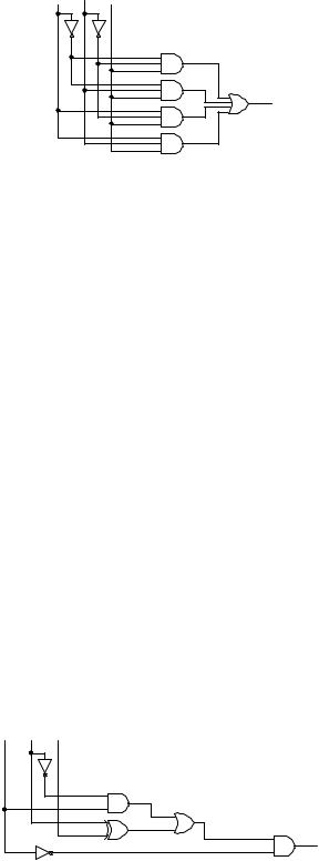
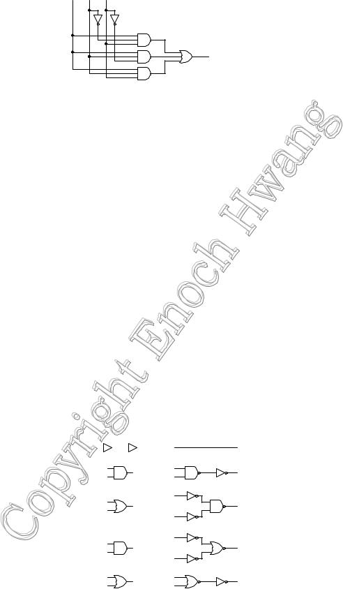
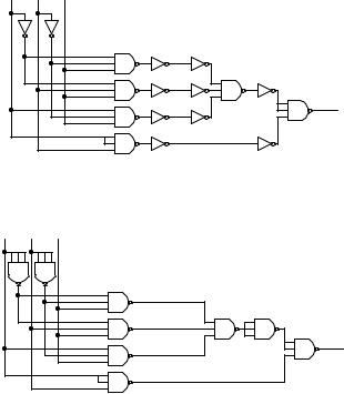
As an example, let us convert the following circuit to use only 3-input NAND gates.
x |
y |
z |
|
|
f |
First, we need to change the 4-input OR gate to a 3- and 2-input OR gates.
x |
y |
z |
|
|
f |
Then we will use Rule 2 to change all the AND gates to 3-input NAND gates with inverters, and Rule 3 to change all the OR gates to 3-input NAND gates with inverters. The 2-input NAND gates are replaced with 3-input NAND gates with two of its inputs connected together.
Microprocessor Design – Principles and Practices with VHDL |
Last updated 7/17/2003 5:56 PM |
Chapter 3 − Combinational Circuits
x |
y |
z |
Page 9 of 26
f
Finally, we eliminate all the double inverters, and replace the remaining inverters with NAND gates with their inputs connected together
x |
y |
z |
|
|
f |
♦
3.4Minimization of Combinational Circuits
When constructing digital circuits, in addition to obtaining a functionally correct circuit, we like to optimize it in terms of circuit size, speed and power consumption. In this section, we will focus on the reduction of circuit size. Usually, by reducing the circuit size, we will also have improved on the speed and power consumption. We have seen in the previous sections that any combinational circuit can be represented using a Boolean function. The size of the circuit is directly proportional to the size or complexity of the functional expression. In fact, it is a one to one correspondence between the functional expression and the circuit size. By using the Boolean algebra theorems, we can transform an expression to another equivalent expression. If the resulting expression is simpler than the original, then we want to implement the circuit based on the simpler expression since that will give us a smaller circuit size.
Using Boolean algebra to transform an expression to one that is simpler is not an easy task, especially for the computer. There is no formula that says which is the next theorem to use. Luckily, there are easier methods for reducing Boolean expressions. The Karnugh map (K-map) method is an easy way for reducing an equation manually and is discussed in section 3.4.1. The Quine-McCluskey or tabulation method for reducing an equation is ideal for programming the computer and is discussed in section 3.4.3.
3.4.1 Karnaugh (K) Maps
To minimize a Boolean equation in the sum-of-products form, we need to reduce the number of product terms by applying the combining Boolean Theorem (Theorem 14) from Section 2.5.1. In so doing we will also have reduced the number of variables used in the product terms. For example, given the following 3-variable function
F = xy'z' + xyz'
we can reduce it to
F= xz' (y' + y)
=xz' 1
=xz'
In other words, two product terms that differ by only one variable whose value is a 0 (primed) in one term and a 1 (unprimed) in the other term, can be combined together to form just one term with that variable omitted as shown
Microprocessor Design – Principles and Practices with VHDL |
Last updated 7/17/2003 5:56 PM |
Chapter 3 − Combinational Circuits |
Page 10 of 26 |
in the example above. Thus, we have reduced the number of product terms and the resulting product term has one less variable. By reducing the number of product terms, we reduce the number of OR operators required, and by reducing the number of variables in a product term, we reduce the number of AND operators required.
Looking at a logic function’s truth table, it is sometimes difficult to see how the product terms can be combined and minimized. A Karnaugh map or K-map for short provides a simple and straight forward procedure for combining these product terms. A K-map is just a graphical representation of a logic function’s truth table where the minterms are grouped in such a way that it allows one to easily see which of the minterms can be combined. It is a 2-dimensional array of squares, each of which represents one minterm in the Boolean function. Thus, the map for an n-variable function is an array with 2n squares.
Figure 3 shows the K-maps for functions with 2, 3, 4, and 5 variables. Notice the labeling of the columns and rows are such that any two adjacent columns or rows differ in only one bit change. This condition is required because we want minterms in adjacent squares to differ in the value of only one variable or one bit, and so these minterms can be combined together. This is why the labeling for the third and fourth columns and the third and fourth rows are always interchanged. When we read K-maps, we need to visualize it as such that the two end columns or rows wrap around so that the first and last columns and the first and last rows are really adjacent to each other because they differ in only one bit also.
In Figure 3 the K-map squares are annotated with its minterm and its minterm number for easy reference only. When we are actually using K-maps to minimize an equation, we will not write these in the squares. Instead, we will be putting 0’s and 1’s in the squares.
Given a Boolean function, we set the value for each K-map square to either a 0 or a 1 corresponding to whether that minterm for the function is a 0-minterm or a 1-minterm. However, since we are only interested in the 1- minterms, the 0’s are sometimes not written in the 0-minterm squares.
x y |
0 |
1 |
|
|
|
|
x yz |
00 |
|
01 |
11 |
10 |
wx yz |
00 |
|
01 |
|
11 |
10 |
|
0 |
1 |
|
|
|
|
|
0 |
1 |
3 |
2 |
|
w'x' 0 |
w'x' 1 |
w'x' 3 |
w'x' 2 |
|||
0 |
x'y' |
x'y |
|
|
|
|
0 |
00 |
|||||||||||
|
|
|
|
x'y'z' |
|
x'y'z |
x'yz |
x'yz' |
y'z' |
|
y'z |
|
yz |
yz' |
|||||
|
|
|
|
|
|
|
|
|
|
|
|
|
|
|
|
||||
|
2 |
3 |
|
|
|
|
|
4 |
5 |
7 |
6 |
|
w'x 4 |
w'x 5 |
w'x 7 |
w'x 6 |
|||
1 |
xy' |
xy |
|
|
|
|
1 |
01 |
|||||||||||
|
|
|
|
xy'z' |
|
xy'z |
xyz |
xyz' |
y'z' |
|
y'z |
|
yz |
yz' |
|||||
|
|
|
|
|
|
|
|
|
|
|
|
|
|
|
|
||||
|
|
|
|
|
|
|
|
|
|
|
|
|
|
12 |
13 |
15 |
14 |
||
|
|
|
|
|
|
|
|
|
|
|
|
|
11 |
wx |
|
wx |
|
wx |
wx |
|
(a) |
|
|
|
|
|
|
|
(b) |
|
|
y'z' |
|
y'z |
|
yz |
yz' |
||
|
|
|
|
|
|
|
|
|
|
|
|
|
|||||||
|
|
|
|
|
|
|
|
|
|
|
wx' |
8 |
wx' |
9 |
11 |
10 |
|||
|
|
|
|
|
|
|
|
|
|
|
|
|
10 |
|
|
wx' |
wx' |
||
|
|
|
|
|
|
|
|
|
|
|
|
|
y'z' |
|
y'z |
|
yz |
yz' |
|
|
|
|
|
|
|
|
|
|
|
|
|
|
|
|
|
||||
|
|
|
|
v = 0 |
|
|
|
|
v = 1 |
|
|
|
|
|
|
|
|
|
|
|
yz |
00 |
|
01 |
|
11 |
10 |
00 |
|
01 |
11 |
10 |
|
|
|
|
(c) |
|
|
|
wx |
|
|
|
|
|
|
|
|
|
|
|
|
|
|
|
|
|
|
|
|
|
0 |
|
1 |
3 |
2 |
|
16 |
17 |
19 |
18 |
|
|
|
|
|
|
|
|
00 |
v'w'x' |
v'w'x' |
v'w'x' |
v'w'x' |
vw'x' |
vw'x' |
vw'x' |
vw'x' |
|
|
|
|
|
|
|
|||
|
y'z' |
|
y'z |
|
yz |
yz' |
y'z' |
|
y'z |
yz |
yz' |
|
|
|
|
|
|
|
|
|
|
|
|
|
|
|
|
|
|
|
|
||||||||
|
01 |
v'w'x4 |
v'w'x5 |
v'w'x7 |
v'w'x6 |
vw'x20 |
vw'x21 |
vw'x23 |
vw'x22 |
|
|
|
|
|
|
|
|||
|
y'z' |
|
y'z |
|
yz |
yz' |
y'z' |
|
y'z |
yz |
yz' |
|
|
|
|
|
|
|
|
|
|
|
|
|
|
|
|
|
|
|
|
||||||||
|
|
12 |
13 |
15 |
14 |
wx |
28 |
29 |
31 |
30 |
|
|
|
|
|
|
|
||
|
11 |
v'wx |
|
v'wx |
|
v'wx |
v'wx |
|
vwx |
vwx |
vwx |
|
|
|
|
|
|
|
|
|
y'z' |
|
y'z |
|
yz |
yz' |
y'z' |
|
y'z |
yz |
yz' |
|
|
|
|
|
|
|
|
|
|
|
|
|
|
|
|
|
|
|
|
||||||||
|
|
v'wx' |
8 |
v'wx' |
9 |
11 |
10 |
|
24 |
25 |
27 |
26 |
|
|
|
|
|
|
|
|
10 |
|
|
v'wx' |
v'wx' |
vwx' |
vwx' |
vwx' |
vwx' |
|
|
|
|
|
|
|
|||
|
y'z' |
|
y'z |
|
yz |
yz' |
y'z' |
|
y'z |
yz |
yz' |
|
|
|
|
|
|
|
|
|
|
|
|
|
|
|
|
|
|
|
|
||||||||
(d)
Figure 3. Karnaugh maps for: (a) 2 variables; (b) 3 variables; (c) 4 variables; (d) 5 variables.
For example, the K-map for the 2-variable function
F = x'y' + x'y + xy
is
Microprocessor Design – Principles and Practices with VHDL |
Last updated 7/17/2003 5:56 PM |