

Finkenzeller K.RFID handbook.2003
.pdf96 |
|
|
|
|
|
|
|
|
|
|
|
|
4 PHYSICAL PRINCIPLES OF RFID SYSTEMS |
|||||||||||||
|
|
|
|
|
|
|
|
|
90 |
|
|
|
|
|
|
|
|
|
|
|
|
|
||||
|
120 |
|
|
|
|
Im in |
Ω |
60 |
|
|
|
|
|
|
|
|||||||||||
|
|
|
|
|
|
|
|
|
|
|
|
|||||||||||||||
|
150 |
|
|
|
|
|
|
|
|
|
|
|
|
30 |
|
|||||||||||
|
|
|
|
|
|
|
|
|
|
|
|
|
|
|
|
|
|
|
||||||||
|
|
|
|
|
|
|
|
|
|
|
|
|
|
|
|
|
|
|
||||||||
|
|
|
|
|
|
|
|
|
|
|
|
|
|
|
|
|
|
fRES > fTX |
RLmax |
|||||||
|
|
|
|
|
|
|
|
|
|
|
|
|
|
|
|
|
|
|
|
|
|
|
||||
|
|
|
|
|
|
|
|
|
|
|
|
|
|
|
|
|
|
|
|
|
|
|
Re in Ω |
|||
|
180 |
|
|
|
|
|
|
|
|
|
|
|
|
|
|
|
|
|
|
|
|
|
|
|
|
0 |
|
|
|
|
|
|
|
|
|
|
0 |
|
5 |
|
10 |
|
15 |
||||||||||
|
|
|
|
|
|
|
|
|
|
|
|
|
|
|
|
|||||||||||
|
|
|
|
|
|
|
|
|
|
|
|
|
RLmin |
|
|
|
|
|
|
|
|
|
|
|
RLmax |
|
|
|
|
|
|
|
|
|
|
|
|
|
|
|
|
|
|
|
|
|
|
|
|
|
|
|
|
|
|
|
|
|
|
|
|
|
|
|
|
|
|
|
|
|
|
fRES < f TX |
|
|
|
|
||||
|
210 |
|
|
|
|
|
|
|
|
|
|
|
|
|
|
|
|
|
330 |
|||||||
|
240 |
|
|
|
|
|
|
|
|
|
300 |
|
|
|
|
|
||||||||||
|
|
|
|
|
|
|
|
|
|
|
|
|
|
|
||||||||||||
|
|
|
|
|
|
|
|
|
|
|
|
|
|
|||||||||||||
|
|
|
|
|
|
|
|
|
|
|
|
|
|
|
|
|
|
|
|
|
|
|
|
|||
|
|
|
|
|
|
fRES = fTX |
270 |
|
|
|
|
|
|
|
|
|
|
|
|
|
||||||
|
|
|
|
|
|
|
|
|
|
|
|
|
|
|
|
|
|
|
|
|
|
|
|
|||
fRES = fTX + 3% fRES = fTX − 1%
Figure 4.35 Locus curve of ZT (RL = 0.3–3 k ) in the impedance plane as a function of the load resistance RL in the transponder at different transponder resonant frequencies
Figure 4.35 shows the corresponding locus curve for ZT = f (RL). This shows that the transformed transponder impedance is proportional to RL. Increasing load resistance RL, which corresponds with a lower(!) current in the data carrier, thus also leads to a greater value for the transformed transponder impedance ZT. This can be explained by the influence of the load resistance RL on the Q factor: a high-ohmic load resistance RL leads to a high Q factor in the resonant circuit and thus to a greater current step-up in the transponder resonant circuit. Due to the proportionality ZT j ωM · i2 — and not to iRL — we obtain a correspondingly high value for the transformed transponder impedance.
If the transponder resonant frequency is detuned we obtain a curved locus curve for the transformed transponder impedance ZT. This can also be traced back to the influence of the Q factor, because the phase angle of a detuned parallel resonant circuit also increases as the Q factor increases (RL ↑), as we can see from a glance at Figure 4.34.
Let us reconsider the two extreme values of RL:
Z |
(R |
0) |
= |
ω2k2 · L1 · L2 |
(4.53) |
|
R2 + j ωL2 |
||||||
T |
L → |
|
|

4.1 MAGNETIC FIELD |
|
|
|
|
|
|
97 |
(‘short-circuited’ transponder coil) |
|
|
|
|
|
|
|
Z (R |
L → ∞ |
) |
= |
ω2k2 · L1 · L2 |
(4.54) |
||
1 |
|
||||||
T |
|
|
|
||||
|
|
|
|
j ωL2 + R2 + |
|
|
|
|
|
|
|
j ωC2 |
|
||
(unloaded transponder resonant circuit). |
|
|
|
|
|||
Transponder inductance L2 |
Let us now investigate the influence of inductance L2 |
||||||
on the transformed transponder impedance, whereby the resonant frequency of the transponder is again held constant, so that C2 = 1/ωTX2 L2.
Transformed transponder impedance reaches a clear peak at a given inductance value, as a glance at the line diagram shows (Figure 4.36). This behaviour is reminiscent of the graph of voltage u2 = f (L2) (see also Figure 4.15). Here too the peak transformed transponder impedance occurs where the Q factor, and thus the current i2 in the transponder, is at a maximum (ZT j ωM · i2). Please refer to Section 4.1.7 for an explanation of the mathematical relationship between load resistance and the Q factor.
4.1.10.3Load modulation
Apart from a few other methods (see Chapter 3), so-called load modulation is the most common procedure for data transmission from transponder to reader by some margin.
|Z ′ | (Ohm) T
35
30
25
20
15
10
5
0 |
× 10−7 |
1 × 10⁻⁶ |
1 × 10⁻⁵ |
1 × 10⁻⁴ |
1 |
fRES = fTX L2 (H) fRES = fTX + 3%
fRES = fTX − 0.5%
Figure 4.36 The value of ZT as a function of the transponder inductance L2 at a constant resonant frequency fRES of the transponder. The maximum value of ZT coincides with the maximum value of the Q factor in the transponder
98 |
4 PHYSICAL PRINCIPLES OF RFID SYSTEMS |
By varying the circuit parameters of the transponder resonant circuit in time with the data stream, the magnitude and phase of the transformed transponder impedance can be influenced (modulation) such that the data from the transponder can be reconstructed by an appropriate evaluation procedure in the reader (demodulation).
However, of all the circuit parameters in the transponder resonant circuit, only two can be altered by the data carrier: the load resistance RL and the parallel capacitance C2. Therefore RFID literature distinguishes between ohmic (or real) and capacitive load modulation.
In this type of load modulation a parallel resistor Rmod is switched on and off within the data carrier of the transponder in time with the data stream (or in time with a modulated subcarrier) (Figure 4.37). We already know from the previous section that the parallel connection of Rmod (→ reduced total resistance) will reduce the Q factor and thus also the transformed transponder impedance ZT. This is also evident from the locus curve for the ohmic load modulator: ZT is switched between the values ZT (RL) and ZT (RL||Rmod) by the load modulator in the transponder (Figure 4.38). The phase of ZT remains almost constant during this process (assuming
fTX = fRES).
In order to be able to reconstruct (i.e. demodulate) the transmitted data, the falling voltage uZT at ZT must be sent to the receiver (RX) of the reader. Unfortunately, ZT is not accessible in the reader as a discrete component because the voltage uZT is induced in the real antenna coil L1. However, the voltages uL1 and uR1 also occur at the antenna coil L1, and they can only be measured at the terminals of the antenna coil as the total voltage uRX. This total voltage is available to the receiver branch of the reader (see also Figure 4.25).
The vector diagram in Figure 4.39 shows the magnitude and phase of the voltage components uZT, uL1 and uR1 which make up the total voltage uRX. The magnitude and phase of uRX is varied by the modulation of the voltage component uZT by the load modulator in the transponder. Load modulation in the transponder thus brings about the amplitude modulation of the reader antenna voltage uRX. The transmitted data is therefore not available in the baseband at L1; instead it is found in the modulation products (= modulation sidebands) of the (load) modulated voltage u1 (see Chapter 6).
Capacitive load modulation In capacitive load modulation it is an additional capacitor Cmod, rather than a modulation resistance, that is switched on and off in time with the data stream (or in time with a modulated subcarrier) (Figure 4.40). This causes the resonant frequency of the transponder to be switched between two frequencies.
i1 |
M |
i2 R2 |
|
Rmod |
|
L1 |
|
L2 |
u2 |
RL |
|
|
|
|
C2 |
S |
Figure 4.37 Equivalent circuit diagram for a transponder with load modulator. Switch S is closed in time with the data stream — or a modulated subcarrier signal — for the transmission of data

4.1 MAGNETIC FIELD |
|
|
|
|
|
|
|
|
|
|
|
|
99 |
|
|
Im in Ω |
|
|
|
|
|
|
|
|
|
|
|
|
|
|
|
|
|
|
|
|
|
|
|
|
Re in Ω |
|
||
|
|
|
|
|
|
|
|
|
|
|
|
|
0 |
|
0 |
|
10 |
|
|
20 |
Z ′ |
(R |
) |
||||||
|
|
|
||||||||||||
|
|
|
|
|
|
|
|
|
|
|
||||
|
Z ′ (R |
||R |
|
) |
|
|
|
T |
|
L |
|
|||
|
mod |
|
|
|
|
|
|
|
||||||
|
T L |
|
|
|
|
|
|
|
|
|
|
|
|
|
330
300
270
Figure 4.38 Locus curve of the transformed transponder impedance with ohmic load modulation (RL||Rmod = 1.5–5 k ) of an inductively coupled transponder. The parallel connection of the modulation resistor Rmod results in a lower value of ZT
Im |
uZT |
uRX
uRX-mod
uL1
uR1 |
Re |
Figure 4.39 Vector diagram for the total voltage uRX that is available to the receiver of a reader. The magnitude and phase of uRX are modulated at the antenna coil of the reader (L1) by an ohmic load modulator
We know from the previous section that the detuning of the transponder resonant frequency markedly influences the magnitude and phase of the transformed transponder impedance ZT. This is also clearly visible from the locus curve for the capacitive load modulator (Figure 4.41): ZT is switched between the values ZT(ωRES1) and ZT(ωRES2) by the load modulator in the transponder. The locus curve for ZT thereby passes

100 |
|
4 PHYSICAL PRINCIPLES OF RFID SYSTEMS |
||
i1 |
M |
R2 |
Cmod |
|
|
i2 |
|
|
|
L1 |
L2 |
u2 |
RL |
|
|
|
C2 |
S |
|
Figure 4.40 Equivalent circuit diagram for a transponder with capacitive load modulator. To transmit data the switch S is closed in time with the data stream — or a modulated subcarrier signal
Re in Ω
0 |
10 |
|
20 |
|
|
|
|
|
|
|
Z ′ |
(C |
) |
|
|
|
|
T |
2 |
|
Z ′ (C |
2 |
+ C |
mod |
) |
|
|
T |
|
|
|
|
||
330
Im in Ω
300
270
Figure 4.41 Locus curve of transformed transponder impedance for the capacitive load modulation (C2||Cmod = 40–60 pF) of an inductively coupled transponder. The parallel connection of a modulation capacitor Cmod results in a modulation of the magnitude and phase of the transformed transponder impedance ZT
through a segment of the circle in the complex Z plane that is typical of the parallel resonant circuit.
Demodulation of the data signal is similar to the procedure used with ohmic load modulation. Capacitive load modulation generates a combination of amplitude and phase modulation of the reader antenna voltage uRX and should therefore be processed in an appropriate manner in the receiver branch of the reader. The relevant vector diagram is shown in Figure 4.42.
Demodulation in the reader For transponders in the frequency range <135 kHz the load modulator is generally controlled directly by a serial data stream encoded in the baseband, e.g. a Manchester encoded bit sequence. The modulation signal from the transponder can be recreated by the rectification of the amplitude modulated voltage at the antenna coil of the reader (see Section 11.3).
In higher frequency systems operating at 6.78 MHz or 13.56 MHz, on the other hand, the transponder’s load modulator is controlled by a modulated subcarrier signal

4.1 MAGNETIC FIELD |
|
101 |
|
|
Im |
uZT |
|
|
|
||
uRX
uRX-mod
uL1
uR1 |
Re |
Figure 4.42 Vector diagram of the total voltage uRX available to the receiver of the reader. The magnitude and phase of this voltage are modulated at the antenna coil of the reader (L1) by a capacitive load modulator
(see Section 6.2.4). The subcarrier frequency fH is normally 847 kHz (ISO 14443-2), 423 kHz (ISO 15693) or 212 kHz.
Load modulation with a subcarrier generates two sidebands at a distance of ±fH to either side of the transmission frequency (see Section 6.2.4). The information to be transmitted is held in the two sidebands, with each sideband containing the same information. One of the two sidebands is filtered in the reader and finally demodulated to reclaim the baseband signal of the modulated data stream.
The influence of the Q factor As we know from the preceding section, we attempt to maximise the Q factor in order to maximise the energy range and the retroactive transformed transponder impedance. From the point of view of the energy range, a high Q factor in the transponder resonant circuit is definitely desirable. If we want to transmit data from or to the transponder a certain minimum bandwidth of the transmission path from the data carrier in the transponder to the receiver in the reader will be required. However, the bandwidth B of the transponder resonant circuit is inversely proportional to the Q factor.
B = |
fRES |
(4.55) |
Q |
Each load modulation operation in the transponder causes a corresponding amplitude modulation of the current i2 in the transponder coil. The modulation sidebands of the current i2 that this generates are damped to some degree by the bandwidth of the transponder resonant circuit, which is limited in practice. The bandwidth B determines a frequency range around the resonant frequency fRES, at the limits of which the modulation sidebands of the current i2 in the transponder reach a damping of 3 dB relative to the resonant frequency (Figure 4.43). If the Q factor of the transponder is

102 |
4 PHYSICAL PRINCIPLES OF RFID SYSTEMS |
′ | (Ohm) T
120
100
80
60
|Z
Modulation products by
load modulation with modulated subcarrier
20 |
|
|
0 |
× 107 1.25 |
× 107 1.3 × 10⁷ 1.35 × 10⁷ 1.4 × 10⁷ 1.45 × 10⁷ 1.5 × 10⁷ |
1.2 |
Q = 15
Q = 30
Q = 60
Figure 4.43 The transformed transponder impedance reaches a peak at the resonant frequency of the transponder. The amplitude of the modulation sidebands of the current i2 is damped due to the influence of the bandwidth B of the transponder resonant circuit (where fH = 440 kHz, Q = 30)
too high, then the modulation sidebands of the current i2 are damped to such a degree due to the low bandwidth that the range is reduced (transponder signal range).
Transponders used in 13.56 MHz systems that support an anticollision algorithm are adjusted to a resonant frequency of 15–18 MHz to minimise the mutual influence of several transponders. Due to the marked detuning of the transponder resonant frequency relative to the transmission frequency of the reader the two modulation sidebands of a load modulation system with subcarrier are transmitted at a different level (see Figure 4.44).
The term bandwidth is problematic here (the frequencies of the reader and the modulation sidebands may even lie outside the bandwidth of the transponder resonant circuit). However, the selection of the correct Q factor for the transponder resonant circuit is still important, because the Q factor can influence the transient effects during load modulation.
Ideally, the ‘mean Q factor’ of the transponder will be selected such that the energy range and transponder signal range of the system are identical. However, the calculation of an ideal Q factor is non-trivial and should not be underestimated because the Q factor is also strongly influenced by the shunt regulator (in connection with the distance d between transponder and reader antenna) and by the load modulator itself. Furthermore, the influence of the bandwidth of the transmitter antenna (series resonant circuit) on the level of the load modulation sidebands should not be underestimated.
Therefore, the development of an inductively coupled RFID system is always a compromise between the system’s range and its data transmission speed (baud

4.1 MAGNETIC FIELD |
103 |
|ZT′| (Ohm)
25
Modulation products by load modulation with modulated
subcarrier
20
15
10
5
0
1.2 × 10⁷ 1.3 × 10⁷ 1.4 × 10⁷ 1.5 × 10⁷ 1.6 × 10⁷ 1.7 × 10⁷
f (Hz)
Q = 10
Figure 4.44 If the transponder resonant frequency is markedly detuned compared to the transmission frequency of the reader the two modulation sidebands will be transmitted at different levels. (Example based upon subcarrier frequency fH = 847 kHz)
rate/subcarrier frequency). Systems that require a short transaction time (that is, rapid data transmission and large bandwidth) often only have a range of a few centimetres, whereas systems with relatively long transaction times (that is, slow data transmission and low bandwidth) can be designed to achieve a greater range. A good example of the former case is provided by contactless smart cards for local public transport applications, which carry out authentication with the reader within a few 100 ms and must also transmit booking data. Contactless smart cards for ‘hands free’ access systems that transmit just a few bytes — usually the serial number of the data carrier — within 1–2 seconds are an example of the latter case. A further consideration is that in systems with a ‘large’ transmission antenna the data rate of the reader is restricted by the fact that only small sidebands may be generated because of the need to comply with the radio licensing regulations (ETS, FCC). Table 4.4 gives a brief overview of the relationship between range and bandwidth in inductively coupled RFID systems.
4.1.11 Measurement of system parameters
4.1.11.1 Measuring the coupling coefficient k
The coupling coefficient k and the associated mutual inductance M are the most important parameters for the design of an inductively coupled RFID system. It is precisely these parameters that are most difficult to determine analytically as a result of the — often complicated — field pattern. Mathematics may be fun, but has its limits.

104 |
4 PHYSICAL PRINCIPLES OF RFID SYSTEMS |
Table 4.4 Typical relationship between range and bandwidth in 13.56 MHz systems. An increasing Q factor in the transponder permits a greater range in the transponder system. However, this is at the expense of the bandwidth and thus also the data transmission speed (baud rate) between transponder and reader
System |
Baud rate |
fSubcarrier |
fTX |
|
Range |
ISO 14443 |
106 kBd |
847 kHz |
13.56 MHz |
0 |
–10 cm |
ISO 15693 short |
26.48 kBd |
484 kHz |
13.56 MHz |
0 |
–30 cm |
ISO 15693 long |
6.62 kBd |
484 kHz |
13.56 MHz |
0 |
–70 cm |
Long-range system |
9.0 kBd |
212 kHz |
13.56 MHz |
0 |
–1 m |
LF system |
−0–10 kBd |
No subcarrier |
<125 kHz |
0 |
–1.5 m |
|
V+ |
|
− |
N1 |
|
Reader coil |
|
|
+ |
R1 |
|
Test transponder |
|
|
|
|
|
coil |
|
|
V− |
VT |
V |
Wave-form generator |
|
|
d |
|
VR |
f0 = 125 kHz
Figure 4.45 Measurement circuit for the measurement of the magnetic coupling coefficient k. N1: TL081 or LF 356N, R1: 100–500 (reproduced by permission of TEMIC Semiconductor GmbH, Heilbronn)
Furthermore, the software necessary to calculate a numeric simulation is often unavailable — or it may simply be that the time or patience is lacking.
However, the coupling coefficient k for an existing system can be quickly determined by means of a simple measurement. This requires a test transponder coil with electrical and mechanical parameters that correspond with those of the ‘real’ transponder. The coupling coefficient can be simply calculated from the measured voltages UR at the reader coil and UT at the transponder coil (in Figure 4.45 these are denoted as VR and VT):
k = Ak · UR |
· |
|
|
LT |
(4.56) |
|
|
UT |
|
|
|
LR |
|

4.1 MAGNETIC FIELD |
105 |
i1 M i2
uTR
LR LT
Cpara |
Ccable Cprobe |
Figure 4.46 Equivalent circuit diagram of the test transponder coil with the parasitic capacitances of the measuring circuit
where UT is the voltage at the transponder coil, UR is the voltage at the reader coil, LT and LR are the inductance of the coils and AK is the correction factor (<1).
The parallel, parasitic capacitances of the measuring circuit and the test transponder coil itself influence the result of the measurement because of the undesired current i2. To compensate for this effect, equation (4.56) includes a correction factor AK. Where CTOT = Cpara + Ccable + Cprobe (see Figure 4.46) the correction factor is defined as:
Ak = 2 − |
1 |
(4.57) |
1 − (ω2 · CTOT · LT) |
In practice, the correction factor in the low capacitance layout of the measuring circuit is AK 0.99 − 0.8 (TEMIC, 1977).
4.1.11.2Measuring the transponder resonant frequency
The precise measurement of the transponder resonant frequency so that deviations from the desired value can be detected is particularly important in the manufacture of inductively coupled transponders. However, since transponders are usually packed in a glass or plastic housing, which renders them inaccessible, the measurement of the resonant frequency can only be realised by means of an inductive coupling.
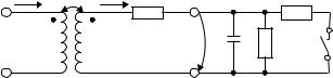
The measurement circuit for this is shown in Figure 4.47. A coupling coil (conductor loop with several windings) is used to achieve the inductive coupling between transponder and measuring device. The self-resonant frequency of this coupling coil should be significantly higher (by a factor of at least 2) than the self-resonant frequency of the transponder in order to minimise measuring errors.
A phase and impedance analyser (or a network analyser) is now used to measure the impedance Z1 of the coupling coil as a function of frequency. If Z1 is represented
i1 M
Z1 |
L1 |
L2 |
? |
Figure 4.47 The circuit for the measurement of the transponder resonant frequency consists of a coupling coil L1 and a measuring device that can precisely measure the complex impedance of Z1 over a certain frequency range