

Fung R.Improving accuracy of ADCs
.pdfImproving Accuracy of Analog-to-Digital Converters
Author: Richard Fung
Date: Nov. 14, 2002
Student Number: 961412560

Abstract – This paper introduces three popular analog-to-digital converter (ADC) architectures to readers: the flash ADC, the multi-step flash ADC, and the pipeline ADC. The fundamental operating principles of these three architectures are described. The specific topic of interest of this paper is methods of improving ADC accuracy. For the flash ADC, the concept of 2X interpolation to increase ADC resolution without significant area/power overhead is described. A design technique in reducing inter-channel mismatch for a time-interleaved multi-step flash ADC is then presented. Finally for the pipeline ADC architecture, a “passive capacitor mismatch error averaging” methodology is illustrated which relaxes capacitor matching requirement, reducing first order mismatch errors to second order.
I. Introduction
With the ever-increasing capability of digital signal processing, many analog signal conditioning are performed in the digital domain today. This is partly due to the fact that the costs associated with digital signal processing are continuing to drop, thanks to the rapid decrease in semiconductor process geometry. As a result of such migration, the need for high accuracy analog-to-digital converters (ADCs) is in high demand where the most accurate digital representation of the analog input signal is desired before performing any type of signal processing.
According to its application, a different kind of ADC is used. Each architecture has its implication on speed, power dissipation, and area, which in turns governs the feasibility of a converter type for a desired accuracy and resolution.
This paper presents three popular types of ADCs: the flash architecture, the multi-step flash architecture, and the pipeline architecture. The design focuses for accuracy for these architectures are also discussed. Finally, examples of techniques in increasing the accuracy of these ADC architectures are discussed. Section II presents to unfamiliar readers with some common specifications that are used to describe an ADC’s performance. In section III, the flash ADC architecture is discussed. A derivative of the flash ADC, the
multi-step flash ADC is presented in section IV. Section V introduces one of the most popular ADC architecture, the pipeline ADC, along with its design considerations. To conclude this paper, section VI briefly discusses about future developments of ADCs.
II. ADC Specifications
The topic of this paper centers around accuracy constraints in analog-to-digital converters, it is logical to first brief the readers in various specifications commonly found describing the performance of an ADC.
A. Quantization Error (QE)
Quantization error is the result of an infinite level analog signal being mapped to a finite number of voltages offered by an ADC with a given resolution. In the case of an ideal ADC, minimization of quantization error at each code step is only possible by increasing the resolution of the ADC. It is given by
QE = Vin − Vstaircase
Vstaircase = D VLSB
where D is the output code of the ADC.
B. Differential Non-Linearity (DNL)
Differential non-linearity describes the error in each voltage step from its previous step, using the ideal step size as a reference. Specifically, it is given by
DNL = Vstep − VLSB
VLSB
Note that DNL is normalized to one LSB. If DNL = -1 LSB, it is guaranteed that a missing code has occurred.
C. Integral Non-Linearity (INL)
The integral non-linearity represents the nonlinearity over the entire range of the ADC. One method of describing INL is by drawing a straight line between the end points of the nonideal ADC transfer function, and the INL is the difference between the code transition points and the straight line. A typical INL curve is shown in Figure 1.
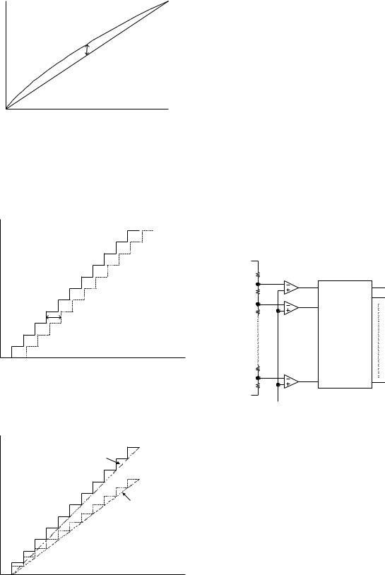
INL
Figure 1: A typical INL curve.
C. Offset Error
An offset error occurs when there is a difference between the value of the first code transition and the ideal value of 0.5 LSB. Note that offset error is constant throughout the entire range of codes. This concept is illustrated in Figure 2.
Offset Error
Figure 2: Offset errors in ADC.
D. Gain Error
When the slope of the transfer characteristic differs from that of an ideal ADC, it is said to have a gain error, shown in Figure 3.
Ideal ADC: K=1
Non-Ideal ADC: K < 1
Figure 3: Gain error of an ADC.
E. Aperture Error
It is a transient effect that introduces errors between the sample and hold modes. In CMOS technology, MOS transistors are used as the switches in the sample and hold circuits. MOS transistors exhibit an input voltage dependent behaviour, where it would not turn off until the condition VG < Vin – Vt is met. As a result, it introduces variation in aperture time (the time it takes to disconnect the sampling capacitor to the analog input voltage source). Note that the aperture error is directly related to the frequency of the input signal, and the worst-case aperture error occurs at the zero crossing (assume the input signal is a sine wave), where dV/dt is the greatest.
III. Flash ADCs
The flash ADC uses an upper and a lower reference voltages, along with a resistor string to generate 2N–1 reference voltages for comparison
with the input voltage, as show in Figure 4.
Vref +
DN-1
DN-2
2N - 1: N
Decoder
D0
Vref -
Vin
Figure 4: Block diagram of flash ADC.
The flash ADC is able to achieve the highest conversion speed, due to the fully parallel approach in its architecture. Each clock pulse generates a digital output word. However, its area doubles for increase in each bit of resolution, where the number of comparators required is 2N-1, rendering it unfeasible for highresolution applications. The large number of comparators at the input also implies a great amount of power dissipation, and large input capacitance. Traditionally, they are limited to 8- bit of resolution.
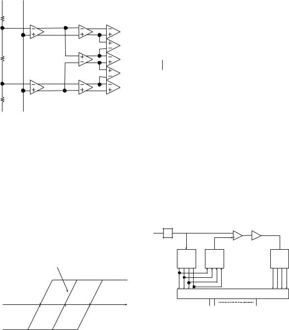
A. 2X Interpolation
One method of reducing the number of comparators and resistor elements used in a flash ADC is by means of interpolation [1]. A 2X interpolation architecture is shown in Figure 5.
Interpolating
Preamplifier Amplifiers
Vin
Figure 5: ADC with interpolation.
Performance indices of the preamplifier such as input common-mode range, input capacitance, power dissipation, overdrive recovery speed, voltage gain, and capacitive feedthrough to the reference resistor ladder often place tight requirements on the preamplifier. Thus, using interpolation to reduce the number of preamplifiers relaxes its design requirements.
The resolution of the flash ADC is increased with interpolation by means of creating additional zero-crossings between preamplifier output levels. This concept is illustrated in
Figure 6.
Interpolated Zero
Crossing
VR,j |
VR,j+1 |
Figure 6: The concept of 2X interpolation.
In [1], it was shown that interpolation also reduces the DNL of the ADC.
B. Accuracy of Flash ADCs
Accuracy of the flash ADC architecture relies on the following:
o Matching of the resistor string.
o Input offset voltage of the comparators o Kickback noise of comparators [1]
With resistor and offset voltage mismatch, the worst case INL occurs at the middle of the string, as calculated as follows [3]:
|
|
|
Vref |
s N −1 |
∆ R |
|
|
|
|
|
|
|
INL |
|
MAX = |
∑ |
K |
+ |
|
VOS,i |
|
MAX |
|||
|
|
|
||||||||||
|
2 |
N |
R |
|
|
|
||||||
|
|
|
|
k =1 |
|
|
|
|
|
|
||
The offset voltage in the comparator is inevitable. However, many designs tend to utilize offset-cancellation techniques in reducing the offset voltages inherent to comparators.
IV. Multi-Step Flash ADCs
A multi-step flash ADC is constructed with two or more flash ADCs cascaded, where the first ADC performs coarse conversion while all other ADCs perform fine conversions separately. It greatly reducing the number of comparators required for the conversion comparing to the flash architecture. However, additional circuitries are required connecting each cascaded flash ADC. The block level diagram is shown in Figure 7.
Subtractor |
Residue Amp |
S/H 
 2N/2
2N/2
|
V1 |
|
|
MSB |
DAC |
LSB |
|
ADC |
ADC |
||
|
|||
MSBs |
|
LSBs |
Latches
Outputs
Figure 7: 2 Step Flash Architecture.
The coarse conversion is done at the first ADC in determining the MSB outputs. The MSB outputs then drive a coarse DAC, regenerating an analog signal that corresponds to the decoded MSB. This resulting signal is then subtracted from the input signal, resulting in a residual
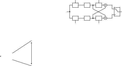
voltage that would be amplified by 2N/2 times. At this point, the amplified signal has a voltage range equivalent to the original input signal. The amplified residual voltage then proceeds to the succeeding stage to obtain the LSB outputs. Since there is a latency between the MSB outputs and the LSB outputs, latches are required to synchronize such delays. It should be noted that utilizing the multi-step flash approach reduces the conversion speed of the converter, since at least 2 conversions are required per input
sample voltage. Figure 8 would better illustrate the operating principle of the 2-step flash ADC.
|
VREF |
|
|
|
VREF |
|
|
|
|
|
|
|
|
|
|||||
11 |
|
|
|
11 |
|
|
|
||
|
|
|
|
|
|
||||
10 |
|
|
|
Subtract and 10 |
|
|
|
||
|
|
|
|
|
|
||||
Vin |
|
|
|
|
Expand by 2N/2 |
|
|||
|
|
|
|
|
|||||
01 |
|
|
|
01 |
|
|
|
||
|
|
|
|
|
|
||||
00 |
|
|
|
00 |
|
|
|
||
|
|
|
|
|
|
||||
|
|
Coarse |
|
Fine |
|||||
|
|
Conversion |
Conversion |
||||||
Figure 8: The ideal behind the 2-step flash ADC.
A. Accuracy of 2-Step Flash ADCs
The accuracy of the 2-step flash ADC is dependent primarily on the linearity of the first ADC in the chain. The reason behind this is that if the first ADC determines the incorrectly the range of the input voltage, then the second ADC stage must be operating in the incorrect range. Therefore, the first ADC must possess the accuracy of the overall converter (i.e. If 8-bit accuracy is desired in a 4-4 2-step flash ADC, the first 4 bit ADC must have 8-bit resolution whereas the second ADC only require 4-bit resolution).
The additional circuitries in the 2-step flash ADC also determine the accuracy of the converter. The subtractor and the residue amplifier must add and amplify the signal to within 1/2 LSB of the ideal value. This would hint that the linearity of the amplifier must be considered.
B. Interchannel Mismatch Error Averaging Technique
In [7], the author described an error averaging technique as a solution to the interchannel mismatch problem in high speed interleaved
ADC for video applications. The circuit used in error averaging is shown in Figure 9.
CLK |
|
CLKB |
S/H |
A/D |
D-1 |
|
|
Delay |
Input |
|
Output |
|
|
Delay |
S/H |
A/D |
Output Select |
D-1 |
||
CLKB |
|
CLK |
Figure 9: Averaged parallel sampling block diagram.
The author also described this topology as feedforward two-tap averaging of parallel signal.
On alternate clock phase, the input signal is sampled by either of the parallel channels. After the analog-to-digital conversion, the resulting signal goes through a one tap delay (denoted by the D-1 element) and summed with the signal in the opposite channel to compensate for interchannel mismatches. At the output select block, the two parallel signals are multiplexed to the output at double the sampling rate. The author stated that this averaging methodology reduces the effective input bandwidth of the sampler [7].
The concept behind this averaging technique exploits the memory aspect of the delay element, and utilizes the inter-channel mismatch error from the previous ½ cycle to average the signal errors in the current cycle on the parallel channel. It should be noted to readers that in time-interleaved ADCs, the jitter requirements of the 2-phase clock pose performance implications on the ADC. Incorrect sampling time on parallel channels would result in distortions in the sampled waveform.
V. Pipeline ADCs
The pipeline ADC takes the 2-step flash ADC and expands it to N-cascaded converters, with one or more bits being converted at each stage. Each pipeline stage has its own sample-and-hold circuit. It is capable of achieving high resolution at relatively high speed, while preserving the low power aspect without significantly decreasing the conversion time. Since inter-stage gain elements are used to achieve nearly identical signal swing at each stage, identical circuits could be used in
each stage of the pipeline. Figure 10 shows the block diagram of a typical pipeline ADC.
Vin S/H |
|
|
|
Vref/2 |
X2 |
S/H |
X2 |
S/H |
|
Vref/2 |
|
Vref/2 |
|
|
DN-1 |
|
DN-2 |
|
D0 |
Figure 10: Block diagram of a pipeline ADC.
Each pipeline stage consist of the following: a S/H circuit, a sub ADC, a DAC, and a differencing fixed-gain amplifier [2]. An advantage of this architecture is that each stage has the full analog-signal sample time period to perform its S/H and partial conversion, which significantly reduces the required speed of the conversion circuits. A disadvantage of this type of converter is that a S/H circuit must be present at each stage of the pipeline, which results in power overhead on the converter. As a result, for a low power design, the converter must employ a low power S/H.
A. Accuracy of Pipeline ADCs
Like the multi-step flash ADC, the pipeline ADC has a dependency on the most significant stage for accuracy, due to the propagation characteristics of the pipeline. Going down the pipeline, each succeeding requires less accuracy than the stage preceding it.
The number of bits per stage greatly affects the overall performance of the pipeline ADC [8]. By lowering the number of bits per stage, the power dissipation of the overall converter is reduced. Increasing the number of bits per stage would increase the converter’s overall linearity. One method of increasing overall linearity while minimizing power is to increase a pipeline stage’s resolution by adding redundancy. A 1.5 bit per stage means one bit is converted along with a ½ bit of redundancy.
The major sources of error of the pipeline ADC are as follows:
•Capacitor mismatch
•Comparator offset voltages
•Sample-and-hold offset voltages
•Gain errors in the inter-stage amplifiers
•Sub ADCs nonlinearity
•Sub DACs nonlinearity
•Opamp settling time errors
For the pipeline architecture, the opamps within the S/H amplifiers limit the speed of the pipelined converters.
In [2], the authors stated that the gain error in the first stage S/H circuit changes the conversion range of the ADC, but does not affect linearity. However, the equivalent error that combines the gain error in the inter-stage amplifier and second stage S/H does affect linearity. The effect of this gain error is small due to the lower resolution requirements required by stages following the first stage. A method of reducing or eliminating the offset errors, gain errors, and sub ADC nonlinearity is the use of digital correction [2]. In this case, the sub DAC non-linearity and opamp settling time error limits the performance of the overall converter.
B. Digital Correction
For high speed ADCs that achieves more than 10 bits of resolution, a technique called digital correction is often used. Its operating principle is by adding redundancy to two neighboring ADC output stages. It is named as such because the final correction to the ADC output is a digital logic computational operation. For example, if only 2 stages are in the pipeline of the ADC, the LSB output would overlap the MSB output by a pre-defined number of bits. The LSBs are then added to or subtracted from the MSBs according to their weighting at the overlap bit to compute the final digitally corrected value of the input analog signal.
C. Capacitor Matching Considerations
In the mismatch point of view, large capacitors match better and would result in more accurate circuits. However, large capacitors increases power dissipations.
One solution to the capacitor-matching problem with smaller size capacitors is the use of calibration [8]. However, it represents overhead in additional circuitries required to perform calibration, and its disadvantage out-weights its advantage at some point. In [8], the author proposed inter-stage scaling of capacitors, where the capacitor sizes are scaled according to the accuracy and noise level requirements. Going down the pipeline, the capacitor matching and noise requirements are relaxed as a result of the reduced in required accuracy. By scaling the
capacitor sizes for each stage, considerable amount of power is saved.
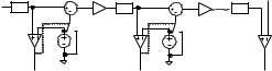
D. Active and Passive Capacitor Mismatch Error-Averaging
One major source of error in pipeline ADCs that uses switched-capacitor circuits is the mismatch of the capacitors. The INL of the pipeline architecture strongly relies on their matching [5].
A technique called capacitor mismatch error averaging was first introduced by Song [6] et al. in 1988. The idea originally presented interchanges the roles of two sampling capacitors during the amplification phase, generating two residue voltages that contain complementary errors. The subsequent stage opamp then proceeds to average the two residue voltages. This method is capable of obtaining excellent linearity with poorly matched capacitors. Although this capacitor mismatch error averaging technique greatly reduces the capacitor-matching requirement (thus reducing the size of the sampling capacitors), it does represent overhead in other circuit complexity in terms of additional averaging amplifiers and capacitors.
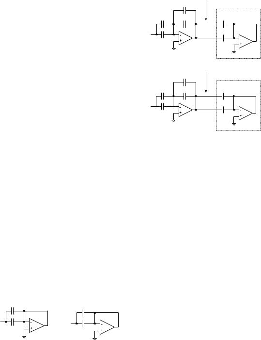
A passive capacitor mismatch error averaging technique based on the above active capacitor mismatch error averaging technique was described in [5]. The author observed that the essence of correcting the mismatch error is to generate a pair of complementary residue voltages and cancel the errors through averaging. Using a passive technique, the overhead of the additional averaging amplifier was taken out. The concept is shown in Figure 11.
Sampling Phase 1 |
Sampling Phase 2 |
C1' |
C1'' |
|
Vin' |
|
Vin'' |
|
C2' |
C2'' |
|
|
C1' = C1'' = C/2
C2' = C2'' = C/2
Figure 11: Passive capacitor error-averaging technique [5].
Vo' = 2Vin - Vref + delta
Transfer Phase 1
C1'
Next Stage
C2' |
C1'' |
C3' |
Vref |
|
|
C2'' |
|
C4' |
|
|
|
C3' = C3'' = C/2 |
|
|
C4' = C4'' = C/2 |
|
Vo'' = 2Vin - Vref - delta |
|
|
|
|
C2' |
Transfer Phase 2 |
|
|
Next Stage |
C1' |
C2'' |
C3'' |
Vref |
|
|
C1'' |
|
C4'' |
|
|
Figure 12: Transfer phase of the erroraveraging technique.
There are two pairs of capacitors and an opamp in the residue amplifier.
The sampling phase 1 samples Vin’ produced by the previous stage onto C1’ and C2’. The sampling phase 2 samples Vin’’ onto C1’’ and C2’’. The transfer phase 1 follows, having C1’ and C1’’ connected in the feedback loop generating the first output residue voltage Vo’ and sampled by the first pair of capacitors C3’ and C4’ in the next stage. In transfer phase 2, the C1 and C2 capacitors are swapped generating the second output residue voltage Vo’’. This voltage is sampled across the second set of sampling capacitors C3’’ and C4’’ in the subsequent stage. The sequence of operation described above is essentially performing double sampling and double integration, which is performed by each stage of the pipeline repetitively. The double sampling at the input of the converter is not required, but is essential for all subsequent stages in order to achieve the error averaging effect.
If each capacitor is associated with a mismatch
coefficient δ , where C1’ = 0.5C(1+ δ 1), then the pair of output voltages could be expressed as follows:
Vo’=(2Vin-Vref)+λ 1(Vin-Vref)+λ 2’(Vin-Vref)+λ 3∆ Vin
Vo’’=(2Vin-Vref)-λ 1(Vin-Vref)+λ 2’’(Vin-Vref)+λ 3∆ Vin
Where

λ1 = 0.5 (δ 2’ + δ 2’’ -δ 1’ - δ 1’’)
λ3 = 0.5 (δ 1’ + δ 2’ -δ 1’’ - δ 2’’)
λ2’ = 0.25 (δ 1’ + δ 1’’) (δ 1’ + δ 1’’ - δ 2’ - δ 2’’)
λ2’’ = 0.25 (δ 2’ + δ 2’’) (δ 2’ + δ 2’’ - δ 1’ - δ 1’’)
The author made the following important observations from the above equations:
•The residue voltages contain first order error that is suppressed to the second order by the averaging effect, provided the errors are complementary.
•The pair of output residue voltage only contains error terms generated by itself (λ 1 terms), and are complementary.
The gain error due to capacitor mismatch could be further expressed as follows, assuming C3’=0.5C(1+δ 3’) and C3’’=0.5C(1+δ 3’’):
Vo = Vo 'C3'+Vo ''C3'' = (2 +ε )Vin −(1+ε )VREF C3 '+C3''
The gain error term in the above term is
ε =18(δ1'+δ1"−δ 2'−δ 2")(δ1'+δ1"−δ 2'−δ 2"−2δ3'+2δ3")
If all δ terms are uncorrelated, then E[ε ]=σ 2/2 and var(ε )=σ 4. The author noted that the positive mean of the gain error introduced by averaging tends to cancel out the negative gain error caused by opamp finite dc gain effect. The speed requirement of comparator in the proposed circuit is also relaxed; with only second order mismatch error in capacitors.
Interested readers could refer to [5] for a second technique in achieving passive capacitor mismatch averaging that yields different expressions in the residue output voltages and gain error.
VI. Future Development
There is no single ADC architecture that is suitable for high speed, high-resolution applications while maintaining low power and small area requirements. The challenge in future ADC designs would be at the architectural level, where such requirements and constraints are met. This is due to the fact that the fundamental limits of existing ADC architectures are well
understood, for which new design techniques are only able to further enhance the accuracy of a given architecture. The groundbreaking ADC architecture that simultaneously meets all critical design parameters is yet to be discovered.
VII. Conclusion
Three different ADC architectures were presented in this paper, along with various methodologies to improve their accuracy. When all parameters are optimized in a given design, it is often the inevitable mismatch that limits a converter’s accuracy. Several approaches to minimizing mismatch errors were presented in this paper, while many other methods exist in the ADC design community.
References
[1] Yun-Ti Wang and Behzad Razavi, “An 8-Bit 150-MHz CMOS A/D Converter”, IEEE J. Solid-State Circuits, vol. 35, pp. 308-317, Mar. 2000
[2]Stephen H. Lewis and Paul R. Gray, “A Pipelined 5- Msample/s 9-bit Analog-to-Digital Cconverter”, IEEE J. Solid-State Circuits, vol. 22, pp. 954-961, Dec. 1987
[3]R. Jacob Baker, Harry W. Li, and David E. Boyce, “CMOS Circuit Design, Layout, and Simulation”, IEEE Press, 1998
[4]David F. Hoeschele, “Analog-to-digital and Digital-to- Analog Conversion Techniques”, John Wiley & Sons, 1994
[5]Yun Chiu, “Inherently Linear Capacitor Error-Averaging Techniques for Pipelined A/D Conversion”, IEEE Trans On
Circuits And Systems II: Analog and Digital Signal Processing, Vol. 47, 3, Mar. 2000
[6] B.-S. Song, M. F. Tompsett, and K. R. Lakshmikumar, “A 12-bit 11-Msample/s capacitor error-averaging pipelined A/D converter,” IEEE J. Solid-State Circuits, vol. 23, pp. 1324-1333, Dec. 1988
[7]K. Nakamura, M. Hotta, L.R. Carley, and D.J. Allstot, “An 85 mW, 10B, 40 Msample/s CMOS Parallel-Pipelined ADC”, IEEE J. Solid-State Circuits, vol. 30, no. 3, Mar. 1995
[8]J.H. Hall and D.G. Nairn, “A 100mW 10 Bit 100MS/S All CMOS ADC”, Advanced A/D and D/A Conversion Techniques and their Applications, 27-28 July 1999 Conference publication No. 466, pp. 5-8, Jul 1999