


104 Radio Engineering for Wireless Communication and Sensor Applications
nl g /2 from the junction. If a 1 = 1 and a2 = 0, then b1 = r = |
||||||||||
(Z 02 |
− Z 01 )/(Z 01 + Z 02 ) = S11 . The voltage transmission coefficient |
|||||||||
is t = 1 + r. The normalized voltage wave b2 |
is obtained from t |
|||||||||
by |
using |
(5.11) and |
(5.12): b2 = (1 |
+ r) √Z 01 /Z 02 = |
||||||
2 |
√ |
Z 01 Z 02 |
|
/(Z 01 + Z 02 ) = S21 . Correspondingly, if a1 |
= 0 and a2 |
|||||
= |
1, S22 |
= r and b1 |
= (1 − r) √Z 02 /Z 01 = 2 |
√ |
Z 01 Z 02 |
/ |
||||
(Z 01 |
+ Z 02 ) = S12 , which may also be recognized directly due to |
|||||||||
the reciprocity.
• A load having an impedance of Z L is a one-port circuit. Its scattering matrix has only one scattering parameter: S11 = r L = (Z L − Z 0 )/ (Z L + Z 0 ), the voltage reflection coefficient of the load terminating a transmission line.
The measurement of scattering parameters is much easier than the measurement of the Z - or Y -parameters. For example, S11 is obtained by measuring the voltage reflection coefficient r1 = b1 /a1 at port 1, as all the other ports are terminated with their characteristic impedance Z 0i and therefore a2 . . . an = 0. It is also an advantage that changing the position of a reference plane only changes the phases of the scattering parameters. For example, if the reference plane of port 1 of a two-port is moved outward
an electrical distance of bl = u, S11 changes to e −2juS11 , S12 to e −juS12 , and S21 to e −juS21 , while S22 remains unchanged.
The transmission matrix [T ] relates the input waves to output waves.
Thus, in the case of a two-port we have |
|
|
|||
Fa2 G FT21 |
T22 GFb1 G |
|
|||
b2 |
= |
T11 |
T12 |
a1 |
(5.19) |
|
|
|
|
||
The transmission matrix is calculated from the scattering parameters as
[T ] = |
F |
S21 − S11 S22 /S12 |
S22 /S12 |
G |
(5.20) |
|
−S11 /S12 |
1/S12 |
|||||
|
|
The transmission matrix of a circuit consisting of blocks connected in series is obtained by multiplying the transmission matrices of the blocks.
5.3 Signal Flow Graph, Transfer Function, and Gain
A signal flow graph [7–9] is a graphical representation of the scattering matrix. It illustrates the equations governing the operation of a circuit. The
Microwave Circuit Theory |
105 |
equations for such transfer functions as gain and reflection coefficient can be derived with the aid of signal flow graphs. Even the analysis of a circuit, which has more than one internal reflection leading to an infinite number of reflected waves, may be kept clear using a signal flow graph.
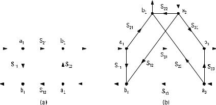
In a flow graph, there are two nodal points for each port. The values of the voltage waves, ai and bi , are assigned to these nodes. The nodes are connected with branches whose gains correspond to the scattering parameters. Signal may flow between two nodes along a branch only to that direction given by the arrow, that is, from node a to node b. Figure 5.5 shows the signal flow graphs for a two-port and three-port.
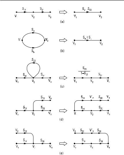
A given transfer function can be solved from a signal flow graph by using the simplification rules explained here and shown in Figure 5.6 [7]:
•Two branches in a series, Figure 5.6(a), with no other branches connected to the common node, can be replaced with one branch whose gain is the product of the gains of the two branches:
V3 = S32 V2 = S32 S21 V1 |
(5.21) |
The normalized voltage waves ai and bi are denoted here with Vi .
•Two branches in parallel, Figure 5.6(b), can be replaced with a single branch whose gain is the sum of the gains of the two branches:
|
V2 = SaV1 + SbV1 = (Sa + Sb ) V1 |
(5.22) |
||||||
|
|
|
|
|
|
|
|
|
|
|
|
|
|
|
|
|
|
|
|
|
|
|
|
|
|
|
|
|
|
|
|
|
|
|
|
Figure 5.5 Signal flow graph for (a) a two-port and (b) a three-port.
106 Radio Engineering for Wireless Communication and Sensor Applications
Figure 5.6 Simplification of flow graphs: (a) branches in series; (b) branches in parallel;
(c) self-loop; (d) duplication of node with duplication of feeding branch; and
(e)duplication of node with duplication of leaving branch.
•A self-loop connected to a node can be eliminated, if the gain of the branch(es) feeding the node is divided by 1 minus the gain of
the loop, because from V2 = S21 V1 + S22 V2 it follows
V2 |
= |
|
S21 |
|
V1 |
(5.23) |
|
1 |
− S22 |
||||||
|
|
|
|
||||

Microwave Circuit Theory |
107 |
•A node can be duplicated by duplicating the branch(es) feeding the node, Figure 5.6(d), or by duplicating the branch leaving the node, Figure 5.6(e).
The following examples illustrate how flow graphs can be simplified and transfer functions solved.
Example 5.1
Derive the input reflection coefficient r in for a two-port when the output port (port 2) is terminated with a load impedance Z L . The characteristic impedance of both ports is Z 0 .
Solution
The voltage reflection coefficient for the load is rL = (Z L − Z 0 )/(Z L + Z 0 ). This is also the gain of the branch connected to the output port in the flow graph of Figure 5.7(a). The node a2 is then duplicated by duplicating the branch rL [Figure 5.7(b)]. The gain of the self-loop is S22 rL according to the rule of branches in series. Then the self-loop is eliminated [Figure 5.7(c)].
Figure 5.7 Solving the input reflection coefficient for a two-port using a flow graph and its simplification rules: (a) a flow-graph presentation of a terminated two-port;
(b) duplication of a node; (c) elimination of a self-loop; and (d) combination of branches in a series.
108 Radio Engineering for Wireless Communication and Sensor Applications
The rule of branches in series is used again [Figure 5.7(d)]. The input reflection coefficient is obtained by applying the rule of branches in parallel:
rin = S11 |
+ |
S21 S12 rL |
(5.24) |
|||
1 |
− |
S22 rL |
||||
|
|
|
||||
Example 5.2
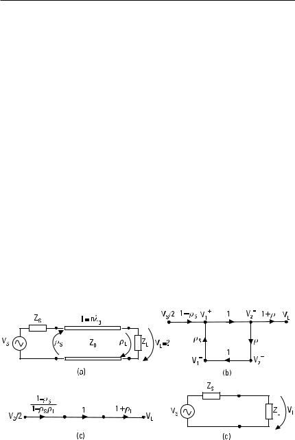
A lossless transmission line is connected between a generator and load. The length of the line is l = nl g (n is integer) and its characteristic impedance is Z 0 , Figure 5.8(a). The load impedance is Z L . The output impedance of the generator is Z S . What is the load voltage VL , if the generator voltage is VS ?
Solution
It is not necessary to normalize the voltages because both ports of the line (two-port) have the same characteristic impedance. The branches representing S11 and S22 are not drawn in Figure 5.8(b) because their gain is zero. Now S21 = S12 = e −jbl = 1. The node having a voltage of VS /2 represents the generator because this voltage corresponds to available power of VS2 /(8Z S ) of the generator. The voltage transmission coefficient from the generator to the line is 1 − rS . A branch having a gain of 1 + r L is added for the calculation of the load voltage VL . By duplicating the node V2−, using the rule of branches in series, and eliminating the self-loop, the flow graph of Figure 5.8(c) is obtained. From this we get
Figure 5.8 Solving the load voltage using flow graphs: (a) a terminated nl g transmission line fed from a generator; (b) its flow-graph presentation; (c) elimination of a self-loop; and (d) an equivalent circuit of the flow graph presented in (c), equivalent to the circuit in (a).

Microwave Circuit Theory |
109 |
|||||
VL = |
(1 − r S ) (1 + r L ) |
× |
VS |
|||
1 |
− rS rL |
|
2 |
|
||
|
|
|
||||
Because the reflection coefficients are rS = (Z S − Z 0 )/(Z S + Z 0 ) and rL =
(Z L − Z 0 )/(Z L + Z 0 ), the load voltage is VL = Z L VS /(Z S + Z L ), which may be seen also from Figure 5.8(d) by using voltage division.
5.3.1 Mason’s Rule
Instead of the flow graph simplification, transfer functions can also be found by using Mason’s rule [10]. According to Mason’s rule, the ratio of a dependent variable (voltage of a node) to an independent variable produced by a source (voltage of the feed node) is
P1 F1 − ∑L (1)1 + ∑L (2)1 − . . .G
+P 2 F1 − ∑L (1)2 + ∑L (2)2 − . . .G + P 3 [1 − . . . ]
T =
1 − ∑L (1) + ∑L (2) − ∑L (3) + . . .
(5.25)
where
P 1 , P 2 , . . . are the gains of the forward paths between the input and output nodes;
SL (1), SL (2), . . . are the sums of the loop gains of the first order, second order, and so on;
SL (1)1, SL (2)1, . . . are the sums of the loop gains of the first order, second order, and so on, for such loops, which do not touch path 1; SL (1)2, SL (2)2, . . . are the sums of the loop gains of the first order, second order, and so on, for such loops, which do not touch path 2.
A path is a continuous succession of branches having arrows pointing to the same direction. It is either a forward path connecting the input node to the output node, or a loop, which originates and terminates on the same node. A path passes each node in the loop only once. The path gain is the product of all the gains in the path. The loop gain is the product of the gains in the loop. The loop gain of the first order means the gain of an individual loop; the loop gain of the second order means the product of the
110 Radio Engineering for Wireless Communication and Sensor Applications
gains of two nontouching loops, and so on. Nontouching loops are separate loops that do not touch each other at any node.
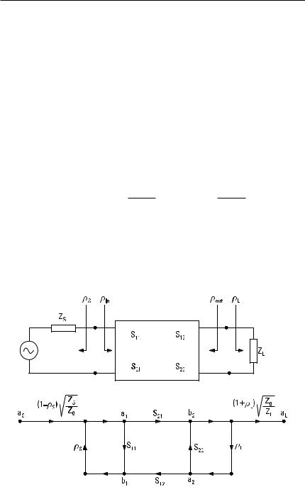
Example 5.3
A generator and a load are connected to a two-port, the transducer power gain, that is, the ratio of the load, P L , to the available power of the generator, P impedance is Z 0 .
as in Figure 5.9. Find power coupled to the S , a . The characteristic
Solution
In the flow graph, aS and aL are normalized voltages corresponding to the available power of the generator and the power coupled to the load, respectively. There is only one path from the input node aS to the output node aL . Its gain is
P 1 = (1 − r S ) √Z S /Z 0 S21 (1 + r L ) √Z 0 /Z L
There are three loops, and the sum of their gains is
∑L (1) = S11 rS + S22 rL + S21 rL S12 r S
The loops S11 rS and S22 r L are nontouching; thus,
Figure 5.9 Two-port connected between a generator and a load.

Microwave Circuit Theory |
111 |
∑L (2) = S11 r S S22 r L
All loops touch path P 1 and therefore
∑L (1)1 = ∑L (2)1 = . . . = 0
Using (5.25), the voltage of the output node is
(1 − r S ) S21 (1 + rL ) √Z S /Z L
aL = 1 − S11 rS − S22 rL − S21 rL S12 rS + S11 rS S22 rL × aS
5.3.2 Gain of a Two-Port
The final expression of the above solution gives us a good basis to present different definitions of the gain of a two-port. The transducer power gain (Gt ) can be presented in several ways:
Gt = |
P L |
= |
| aL |2 |
= |
|
| S21 |2 X1 − | r S |2 CX1 − | r L |2 C |
||||||
|
|
|
|
|
|
|
|
|||||
P S, a |
| aS |2 |
|
| (1 |
− S11 rS ) (1 |
− S22 rL ) − S12 S21 rS rL |2 |
|||||||
|
|
|
|
|||||||||
= |
|
| S21 |2 X1 − | r S |2 CX1 − | rL |2 C |
(5.26) |
|||||||||
|
| 1 − r S r in |2 | 1 − S22 r L |2 |
|
||||||||||
= |
|
| S21 |2 X1 − | r S |2 CX1 − | rL |2 C |
|
|
||||||||
|
| 1 − S11 rS |2 | 1 − rout r L |2 |
|
|
|
||||||||
where r out is the reflection coefficient of the output port 2.
The power gain (Gp ) of a two-port is defined as the ratio of the power coupled to the load, P L , to the power coupled to the two-port, P in . Using the flow graph we obtain
Gp = |
P L |
= |
|
| aL |2 |
= |
|
| S21 |2 X1 − | r L |2 C |
|
Pin |
| a1 |
|2 X1 − | rin |2 C |
| 1 |
− S22 rL |2 X1 − | rin |2 C |
||||
|
|
|
(5.27)
The available power gain (Ga ) is defined as the ratio of the available output power of the two-port, Pout , a , to the available power of the generator,
P S , a :
112 Radio Engineering for Wireless Communication and Sensor Applications
Ga = |
Pout , a |
= |
P L ( r L = r out* |
) |
= |
|
| S21 |2 X1 − | rS |2 C |
|
P S, a |
|
P S, a |
|
| 1 |
− S11 rS |2 X1 − | rout |2 C |
|||
|
|
|
|
|
||||
(5.28)
The maximum available power gain (Ga, max ) is the available power gain in that case when the input port is conjugate-matched to the generator:
Ga , max = |
P L ( rL = r out* |
) |
||
|
|
(5.29) |
||
Pin ( rS = r in* |
) |
|||
|
|
|||
How Ga, max can be expressed using the scattering parameters of a two-port is presented in Chapter 8, (8.28). In a unilateral case (S12 = 0), the maximum available power gain is
Ga , max = |
|
| S21 |
|2 |
(5.30) |
|
X1 |
− | S11 |2 CX1 − | S22 |2 C |
||||
|
|
||||
The insertion gain (Gi ) is the ratio of the power coupled to the load from the two-port, P L , to the power coupled to the load directly from the generator, P d (no two-port between):
Gi = |
P L |
= |
| S21 |
|2 |1 − rS rL |2 |
(5.31) |
|
P d |
|1 − rS rin |2 |1 − S22 r L |2 |
|||||
|
|
|
||||
If both the generator and load are matched to the characteristic impedance
Z 0 , r S = rL = 0 and Gi = | S12 | 2. The inverse of Gi is called the insertion loss:
L i = |
1 |
= |
P d |
(5.32) |
|
Gi |
P L |
||||
|
|
|
The insertion gain and insertion loss are parameters, which can be measured directly. Other gains of a two-port may be calculated from measured scattering parameters and impedances Z S and Z L .
Microwave Circuit Theory |
113 |
References
[1]Kuh, E. S., and R. A. Rohrer, Theory of Linear Active Networks, San Francisco, CA: Holden-Day, 1967.
[2]Lay, D. C., Linear Algebra and Its Applications, 3rd ed., Reading, MA: Addison Wesley, 2002.
[3]Collin, R. E., Foundations for Microwave Engineering, 2nd ed., New York: IEEE Press, 2001.
[4]Ramo, S., J. Whinnery, and T. van Duzer, Fields and Waves in Communication Electronics, New York: John Wiley & Sons, 1965.
[5]Belevitch, V., ‘‘Transmission Losses in 2n -Terminal Networks,’’ Journal of Applied Physics, Vol. 19, No. 7, 1948, pp. 636–638.
[6]Montgomery, C. G., R. H. Dicke, and E. M. Purcell, Principles of Microwave Circuits, Radiation Laboratory Series, New York: McGraw-Hill, 1948.
[7]Kuhn, N., ‘‘Simplified Signal Flow Graph Analysis,’’ Microwave Journal, November 1963, pp. 59–66.
[8]Bryant, G. H., Principles of Microwave Measurements, London, England: Peter Peregrinus, 1988.
[9]Nyfors, E., and P. Vainikainen, Industrial Microwave Sensors, Norwood, MA: Artech House, 1989.
[10]Mason, S. J., ‘‘Feedback Theory: Further Properties of Signal Flow Graphs,’’ IRE Proc., Vol. 44, July 1956, pp. 920–926.
6
Passive Transmission Line and
Waveguide Devices
Transmitters and receivers are composed of many kinds of passive and active devices. Some important passive devices based on sections of transmission lines or waveguides are covered in this chapter. Frequency-selective passive devices, resonators and filters, are the topic of Chapter 7. Standardized symbols for various passive devices are shown in Figure 6.1. Most passive devices are reciprocal; only isolators and circulators, which are based on ferrites, are nonreciprocal.
Components or devices used in radio equipment at various frequency ranges can be divided into three groups, according to their size in wavelengths:
1.Lumped components, such as capacitors and coils, are usable up to UHF and even higher frequencies. Their size is small compared to a wavelength. As the frequency increases, lumped elements become lossy and their parasitic reactances and radiation loss increase. For example, a capacitor may become a resonant circuit as a result of the parasitic inductances of the connecting wires.
2.Distributed components are made of sections of transmission lines or waveguides. Their size is comparable to a wavelength, and the phase differences between the parts of a component are significant. Distributed components are used at microwave and millimeter-wave ranges. However, waveguide components eventually become lossy and difficult to fabricate as the frequency increases.
115