

154 Radio Engineering for Wireless Communication and Sensor Applications
a dielectric resonator is much smaller than the size of a cavity resonator operating at the same frequency. Electric and magnetic fields concentrate within the resonator, but part of the field is outside the cylinder and this part may be employed in coupling. The radiation loss is low and the quality factor is mainly determined by the loss in the dielectric material. The unloaded quality factor Q 0 is typically 4,000 to 10,000 at 10 GHz. A given resonator can operate at several resonance modes, of which the TE01d mode is the most used.
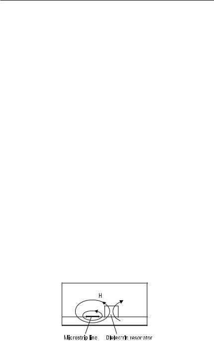
Dielectric resonators are used in filters and transistor oscillators at frequencies from 1 to 50 GHz. If the frequency of an oscillator is stabilized with a dielectric resonator, it is called a dielectric resonator oscillator (DRO). Figure 7.10 shows how a DRO is coupled to a microstrip line. The magnetic fields of the line and the resonator have common components. The resonator is simply placed on the substrate, and the strength of the coupling can be adjusted by changing the distance of the resonator from the strip. To reduce radiation loss, the structure is enclosed within a metal case.
7.2 Filters
A resonator with two couplings passes through signals having frequencies near the resonance frequency; in other words, it acts as a bandpass filter. A hollow metal waveguide acts as a highpass filter, because it has a cutoff frequency that depends on the dimensions.
In general a filter is a two-port, which prevents propagation of undesired signals while desired signals pass it. In an ideal case, there is no insertion loss in the passband, but the attenuation in the stopband is infinite. Depending on the appearance of these bands, the filter is said to be a bandpass, bandstop, lowpass, or highpass filter. An ideal filter has a linear phase response, which allows a signal containing several frequency components to pass through
Figure 7.10 Dielectric resonator coupled to a microstrip line.
Resonators and Filters |
155 |
without distortion. Filters are used also for multiplexing (combining signals at different frequencies) and demultiplexing (separating signals at different frequencies). Also, reactive impedance matching circuits, tuning circuits in oscillators and amplifiers, delay lines, and slow-wave structures act as filters.
In the design of filters, two basic methods are used: the image parameter method and insertion loss method [3, 5, 6]. In the image parameter method, simple filter sections are cascaded to provide the desired passband-stopband characteristics. However, the required frequency response for the whole frequency range cannot be exactly synthesized. An iterative design process is used to improve the frequency response. On the contrary, the insertion loss method allows the synthesis of an exact response. We study the insertion loss method in more detail in the following section.
A filter design using the insertion loss method gives as a result a circuit consisting of lumped elements. At microwave frequencies, distributed elements are used instead of lumped ones as already discussed in Chapter 4. To realize distributed elements corresponding to the desired lumped elements, we use transmission line sections and aid the design with Richards’ transformation, the Kuroda identities, as well as the impedance and admittance inverters.
7.2.1 Insertion Loss Method
In the insertion loss method, the filter design and synthesis is started by choosing the desired frequency response. This is followed by calculation of the normalized (in terms of frequency and impedance) component values for a lowpass filter prototype. These normalized component values can also be obtained from tables presented in the literature [6]. Then the normalized filter is converted to the desired frequency band and impedance level.
The insertion loss of a filter containing only reactive elements is obtained from its reflection coefficient as
L = |
|
1 |
(7.34) |
|
− | r(v) |2 |
||
1 |
|
||
The power reflection coefficient | r(v ) |2 of all realizable linear, passive circuits can be expressed as a polynomial of v2, that is, it is an even function of v . It follows from this fact that the insertion loss of (7.34) can always be written as [3, 7]

156 Radio Engineering for Wireless Communication and Sensor Applications
L = 1 + |
P (v 2 ) |
|
(7.35) |
|
Q 2(v) |
||||
|
|
|||
where P is a polynomial of v 2 and Q is a polynomial of v .
The most frequently used filter responses are the maximally flat and Chebyshev responses. In the following we study these filter responses in more detail.
Maximally Flat Response The maximally flat response is also called the binomial or Butterworth response. It provides the flattest possible passband for a given order of the filter, that is, in practice for a given number of reactive elements. The insertion loss for the lowpass filter prototype is
L = 1 + k 2 S |
v |
D2N |
(7.36) |
vc |
where N is the order of the filter and vc is its cutoff (angular) frequency. Note that here Q 2(v) = 1. The passband is from 0 to vc , and at vc the insertion loss is L = 1 + k 2. Most often the band edge is chosen to be the 3-dB point, and then k = 1. At frequencies well above the cutoff frequency (v >> vc ) the insertion loss is L ≈ k 2(v /vc )2N and, thus, it increases 20N dB per decade.
Chebyshev Response The Chebyshev response is often also called the equalripple response. The insertion loss is
L = 1 + k 2TN2 S |
v |
D |
(7.37) |
vc |
where TN is the N th order Chebyshev polynomial, which can also be written as
TN S |
v |
D = cos FN arccos S |
v |
DG |
(7.38) |
||||
vc |
vc |
||||||||
when 0 ≤ v/vc ≤ 1, and |
|
||||||||
TN S |
v |
D = cosh FN arcosh S |
v |
DG |
(7.39) |
||||
vc |
vc |
||||||||
Resonators and Filters |
157 |
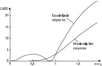
when v/vc ≥ 1. In the passband, L varies between values 1 and 1 + k 2. At v = 0 the insertion loss is L = 1 if N is odd, and L = 1 + k 2, if N is even. When v >> vc , L ≈ k 2(2v/vc )2N /4, which is to say, the insertion loss increases 20N dB per decade, as is also the case with a maximally flat response. The insertion loss is, however, 22N /4 times larger than that of a maximally flat response of the same order. In Figure 7.11 these responses are compared to each other.
Other important filter responses are the elliptic amplitude response and the linear phase response. The insertion loss of the maximally flat and Chebyshev responses increases monotonically in the stopband. In some applications a given minimum stopband insertion loss is adequate but a sharper cutoff response is desired. In such a case an elliptic filter is a good choice [8]. In some other applications (e.g., in multiplexers) a phase response as linear as possible is desired. Then a linear phase filter is the correct choice. However, a good phase response and a sharp cutoff response are incompatible requirements, so in designing a filter for a good phase response one must compromise with the amplitude response.
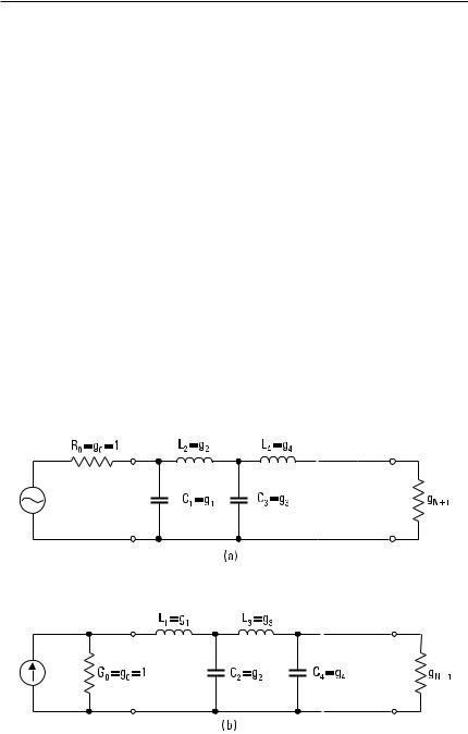
A normalized lowpass filter consists of shunt (parallel) capacitors and series inductors g k . The generator source impedance is g 0 = 1V or the source admittance is g 0 = 1S, depending on whether the filter prototype starts with a shunt capacitor or with a series inductor, respectively, and the cutoff
Figure 7.11 Maximally flat and Chebyshev (equal-ripple) responses of a lowpass filter (N = 3, k = 1).
158 Radio Engineering for Wireless Communication and Sensor Applications
frequency is vc = 1. The order N of the filter is the number of reactive elements in the filter. As already discussed, the first element may be a shunt element, as in Figure 7.12(a), or a series element, as in Figure 7.12(b). The response in both cases is the same. The element g N + 1 is the load resistance if g N is a shunt capacitor, and the load conductance if g N is a series inductor.
With the equivalent circuits presented in Figure 7.12, it is possible to calculate the component values that provide a given response. For the maximally flat response the prototype component values are g 0 = 1, g N + 1 = 1, and
|
F |
2N |
G |
|
g k = 2 sin |
|
(2k − 1)p |
|
(7.40) |
|
|
|
where k = 1 . . . N. For the Chebyshev response, calculation of the component values is more difficult, so we omit it here. Tables 7.1 through 7.3 represent element values for maximally flat and Chebyshev (equal ripple) lowpass filter prototypes.
After the lowpass filter prototype design is completed, the circuit designed is converted to the correct frequency and correct impedance level.
Figure 7.12 Lowpass filter prototypes: beginning with (a) a parallel element, and (b) a series element.
Resonators and Filters |
159 |
Table 7.1
Element Values for the Maximally Flat Lowpass Filter Prototype (g 0 = 1, vc = 1)
N |
g 1 |
g 2 |
g 3 |
g 4 |
g 5 |
g 6 |
g 7 |
|
|
|
|
|
|
|
|
1 |
2.0000 |
1.0000 |
|
|
|
|
|
2 |
1.4142 |
1.4142 |
1.0000 |
|
|
|
|
3 |
1.0000 |
2.0000 |
1.0000 |
1.0000 |
|
|
|
4 |
0.7654 |
1.8478 |
1.8478 |
0.7654 |
1.0000 |
|
|
5 |
0.6180 |
1.6180 |
2.0000 |
1.6180 |
0.6168 |
1.0000 |
|
6 |
0.5176 |
1.4142 |
1.9318 |
1.9318 |
1.4142 |
0.5176 |
1.0000 |
|
|
|
|
|
|
|
|
Source: [6].
Table 7.2
Element Values for a Chebyshev Lowpass Filter Prototype (g 0 = 1, vc = 1, ripple 0.5 dB)
N |
g 1 |
g 2 |
g 3 |
g 4 |
g 5 |
g 6 |
g 7 |
1 |
0.6986 |
1.0000 |
|
|
|
|
|
2 |
1.4029 |
0.7071 |
1.9841 |
|
|
|
|
3 |
1.5963 |
1.0967 |
1.5963 |
1.0000 |
|
|
|
4 |
1.6703 |
1.1926 |
2.3661 |
0.8419 |
1.9841 |
|
|
5 |
1.7058 |
1.2296 |
2.5408 |
1.2296 |
1.7058 |
1.0000 |
|
6 |
1.7254 |
1.2479 |
2.6064 |
1.3137 |
2.4758 |
0.8696 |
1.9841 |
|
|
|
|
|
|
|
|
Source: [6].
Table 7.3
Element Values for a Chebyshev Lowpass Filter Prototype (g 0 = 1, vc = 1, ripple 3.0 dB)
N |
g 1 |
g 2 |
g 3 |
g 4 |
g 5 |
g 6 |
g 7 |
|
|
|
|
|
|
|
|
1 |
1.9953 |
1.0000 |
|
|
|
|
|
2 |
3.1013 |
0.5339 |
5.8095 |
|
|
|
|
3 |
3.3487 |
0.7117 |
3.3487 |
1.0000 |
|
|
|
4 |
3.4389 |
0.7483 |
4.3471 |
0.5920 |
5.8095 |
|
|
5 |
3.4817 |
0.7618 |
4.5381 |
0.7618 |
3.4817 |
1.0000 |
|
6 |
3.5045 |
0.7685 |
4.6061 |
0.7929 |
4.4641 |
0.6033 |
5.8095 |
|
|
|
|
|
|
|
|
Source: [6].
160 Radio Engineering for Wireless Communication and Sensor Applications
If the generator resistance is R 0 , the scaled element values (symbols with prime) are
L k′ = R 0 L k |
(7.41) |
Ck′ = Ck /R 0 |
(7.42) |
R L′ = R 0 R L |
(7.43) |
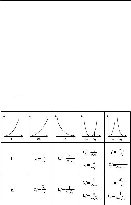
where L k , Ck , and R L are the prototype values g k and g N + 1 . Figure 7.13 shows the scaling of the cutoff frequency from 1 to vc , and the transformations to a highpass, bandpass, and bandstop filter. In a bandpass filter, an LC series circuit corresponds to a series inductor of the lowpass prototype, and an LC parallel circuit corresponds to a shunt capacitor of the lowpass prototype. On the other hand, in a bandstop filter, an LC parallel circuit corresponds to a series inductor, and an LC series circuit corresponds to a shunt capacitor of the lowpass prototype. In the equations for Figure 7.13,
v 0 = √v1 v 2 , D = (v2 − v 1 )/v0 , and v 1 and v2 are the limits of the filter frequency band.
Figure 7.13 |
Frequency scaling and transformations of a lowpass filter prototype, v 0 |
= |
|
√v 1 v 2 , D = (v 2 − v 1 )/v 0 . |
|