

Lm016L
.pdfApplication Notes for Character Mode LCDs |
Page 11 of 24 |
2 x 40
2 x 24
2 x 20
2 x 16
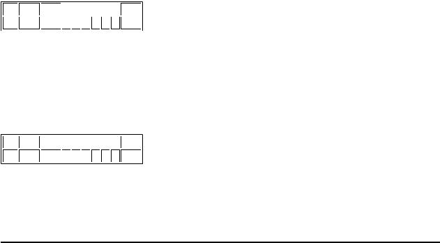
2 x 8
80 81 82 83 84 85 86 87 88 89 8A 8B 8C 8D 8E 8F 90 91 92 93 94 95 96 97 ... A5 A6 A7 C0 C1 C2 C3 C4 C5 C6 C7 C8 C9 CA CB CC CD CE CF D0 D1 D2 D3 D4 D5 D6 D7 ... E5 E6 E7
2 Line Display Addresses
2 x 40
2 x 24
2 x 20
2 x 16
2 x 8
81 82 83 84 85 86 87 88 89 8A 8B 8C 8D 8E 8F 90 91 92 93 94 95 96 97 98 ... A6 A7 80 C1 C2 C3 C4 C5 C6 C7 C8 C9 CA CB CC CD CE CF D0 D1 D2 D3 D4 D5 D6 D7 D8 ... E6 E7 C0
2 Line Display with Display Shifted Left (I/D=1, S=1. See Entry Mode Set Instruction)
F. INSTRUCTION TABLE
|
|
|
|
|
|
|
|
|
|
|
|
Execution |
|
Instruction |
RS R/W DB7 DB6 DB5 DB4 DB3 DB2 DB1 DB0 |
Description |
Time |
||||||||||
(when Fcp or |
|||||||||||||
|
|
|
|
|
|
|
|
|
|
|
|
||
|
|
|
|
|
|
|
|
|
|
|
|
fosc is 250KHz) |
|
|
|
|
|
|
|
|
|
|
|
|
Clears Display and |
|
|
Clear Display |
0 |
0 |
0 |
0 |
0 |
0 |
0 |
0 |
0 |
1 |
returns cursor to the 80uS = |
||
Home Position |
1.64mS |
||||||||||||
|
|
|
|
|
|
|
|
|
|
|
|||
|
|
|
|
|
|
|
|
|
|
|
(Address 00) |
|
|
|
|
|
|
|
|
|
|
|
|
|
Returns cursor to |
|
|
|
|
|
|
|
|
|
|
|
|
|
Home Position. |
|
|
Return Home |
0 |
0 |
0 |
0 |
0 |
0 |
0 |
0 |
1 |
* |
Returns shifted |
40uS = 1.6mS |
|
display to original |
|||||||||||||
|
|
|
|
|
|
|
|
|
|
|
|
||
|
|
|
|
|
|
|
|
|
|
|
position. Does not |
|
|
|
|
|
|
|
|
|
|
|
|
|
clear display |
|
|
|
|
|
|
|
|
|
|
|
|
|
Sets DD RAM |
|
|
|
|
|
|
|
|
|
|
|
|
|
counter to |
|
|
|
|
|
|
|
|
|
|
|
|
|
increment or |
|
|
Entry Mode Set |
0 |
0 |
0 |
0 |
0 |
0 |
0 |
1 |
I/D |
S |
decrement (I/D) |
40uS |
|
Specifies cursor or |
|||||||||||||
|
|
|
|
|
|
|
|
|
|
|
display shift during |
|
|
|
|
|
|
|
|
|
|
|
|
|
to Data Read or |
|
|
|
|
|
|
|
|
|
|
|
|
|
Write (S) |
|
|
|
|
|
|
|
|
|
|
|
|
|
Sets Display |
|
|
Display |
|
|
|
|
|
|
|
|
|
|
ON/OFF (D), cursor |
|
|
ON/OFF |
0 |
0 |
0 |
0 |
0 |
0 |
1 |
D |
C |
B |
ON/OFF (C), and |
40uS |
|
Control |
|
|
|
|
|
|
|
|
|
|
blink character at |
|
|
|
|
|
|
|
|
|
|
|
|
|
cursor position |
|
|
|
|
|
|
|
|
|
|
|
|
|
Moves cursor or |
|
|
Cursor or |
0 |
0 |
0 |
0 |
0 |
1 |
S/C |
R/L |
* |
* |
shifts the display |
40uS |
|
Display Shift |
w/o changing DD |
||||||||||||
|
|
|
|
|
|
|
|
|
|
|
|||
RAM contents 


 Sets data bus
04/09/98

Application Notes for Character Mode LCDs |
Page 12 of 24 |
Function Set |
0 0 |
0 |
Set CG RAM
0 0 0
Address
Set DD RAM
0 0 1
Address
Read Busy Flag |
0 1 BF |
& Address |
|
SIZE=2>Write
Data from DD 1 0 or CG RAM
Read Data from |
1 1 |
DD or CG RAM |
|
I/D=1: Increment
S=1: Display Shift on data entry
S/C=1: Display Shift (RAM unchanged)
R/L=1: Shift to the Right DL=1: 8 bits
N=1: 2 Lines
F=1: 5x10 Dot Font D=1: Display ON C=1: Cursor ON B=1: Blink ON BF=1: Cannot accept instruction
* Don't Care
0 1 DL N F * *
1 |
ACG |
ADD
AC
Write Data
Read Data
I/D=0: Decrements
S=0: Cursor Shift on data entry S/C=0: Cursor Shift (RAM unchanged)
R/L=0: Shift to the Left DL=0: 4 bits
N=0: 1 Line
F=0: 5x7 Dot Font
D=0: Display OFF
C=0: Cursor OFF
B=0: Blink OFF
BF=0: Can accept instruction
length (DL), # of display lines (N), and character font
(F)
Sets CG RAM address. CG RAM data is sent and received after this instruction
Sets DD RAM address. DD RAM data is sent and received after this instruction
Reads Busy Flag (BF) and address counter contents
Writes data to DD or CG RAM and increments or decrements address counter (AC)
Reads data from DD or CG RAM and increments or decrements address counter (AC)
Definitions:
DD RAM: Display data RAM
CG RAM: Character generator RAM
ACG: CG RAM Address
ADD: DD RAM
Address(Cursor
Address) AC: Address
Counter used for both DD and CG RAM Address
40uS
40uS
40uS
1uS
40uS
40uS
Execution Time changes when Frequency changes per the following example:
If FCP or fosc is 27 KHz
40uS x 250/270 = 37uS
G. INSTRUCTION DESCRIPTION
CLEAR DISPLAY
CODE
RS R/W DB7 


 DB0
DB0
0 |
0 |
0 |
0 0 0 0 0 0 1 |
Writes space code "20" (hexadecimal) into all the DD RAM addresses. The cursor returns to Address 0 (ADD="80") and display, if it has been shifted, returns to the original position. In other words, display disappears and the cursor goes to the left edge of the display (the first line if a 2 or 4 line display module is used).
04/09/98

Application Notes for Character Mode LCDs |
Page 13 of 24 |
RETURN HOME
CODE
RS R/W DB7 

 DB0
DB0
0 |
0 |
0 |
0 0 0 0 0 1 * |
* Don't Care
Returns the cursor to Address 0 (ADD="80") and display, if it has been shifted, to the original position. The DD RAM contents remain unchanged.
ENTRY MODE SET
CODE
RS R/W DB7 

 DB0
DB0
0 0 |
0 |
0 0 0 0 1 I/D S |
I/D: Increments (I/D=1) or decrements (I/D=0) the DD RAM address by one when writing or reading a character code from DD RAM. The cursor moves to the right when incremented by one. The same applies to writing and reading CG RAM.
S: Shifts the entire display to either the right or the left when S is 1; to the left when I/D=1 and to the right when I/D=0. Therefore, the cursor looks as if stood stil while only the display has moved. Display is not shifted when reading from DD RAM. Display is not shifted when S=0.
DISPLAY ON/OFF CONTROL
CODE
RS R/W DB7 

 DB0 0 0 0 0 0 0 1 D C B
D: Display is turned ON when D=1 and OFF when D=0. When display is turned off due to D=0, the display data remains in the DD RAM and it can be displayed immediately by setting D=1.
C: The cursor is displayed when C=1 and not displayed when C=0. Even if the cursor disappears, function of I/D, etc. does not change during display data write. The cursor is displayed using 5 dots in the 8th lines when the 5 x 7 dot character font is selected and in the 11th line when 5 x 10 dot character font is selected.
B: The character residing at the cursor position blinks when B=1. The blink is done by switching between all dots ON and display characters at 0.4 second interval. The cursor and the blink can be set concurrently.
Detached |
Attached |
Blinking Character |
Cursor Position
CURSOR OR DISPLAY SHIFT
CODE
RS R/W DB7 

 DB0
DB0
0 0 |
0 |
0 0 1 S/C R/L * * |
* Don't Care
04/09/98

Application Notes for Character Mode LCDs |
Page 14 of 24 |
Shifts the cursor position or display to the right or left without writing or reading the display data. This function is used for correction or search of display.
S/C R/L
0 0
Shifts the cursor position to the left. (AC is decremented by one.)
0 1
Shifts the cursor position to the right. (AC is incremented by one).
1 0
Shifts the entire display to the left.
The cursor follows the display shift.
1 1
Shifts the entire display to the right.
The cursor follows the display shift.
FUNCTION SET
CODE
RS R/W DB7 

 DB0 0 0 0 0 1 DL N F * *
* Don't Care
DL: Sets interface data length. Data is sent or received in 8 bit length (DB7-DB0) when DL=1 and 4 bit length (DB7-DB4) when DL=0. When 4 bit length is selected, data must be sent or received in 2 operations.
N: Sets number of display lines. F: Sets character font.
(Together, N & F set the duty cycle).
SET CG RAM ADDRESS
CODE
RS R/W DB7 

 DB0 0 0 0 1 A A A A A A
Sets the CG RAM address in a binary number of AAAAAA to the address counter, and data is written or read from the MPU related to the CG RAM after this. This is used for programming the Character Generator (CG) RAM.
SET DD RAM ADDRESS
CODE
RS R/W DB7 

 DB0 0 0 1 A A A A A A A
Sets the DD RAM address in a binary number of AAAAAAA in the address counter. Data is written or read from the MPU related to the DD RAM after this. When N=0 (1 line display), AAAAAAA is "00" to "47" (hexadecimal) When N=1 (2 line display),
AAAAAAA for the first line is "00" to "27" and "40" to "67", (hexadecimal) for the second line. Because the MSB is set to "!", the hex codes are actually "80" to "C0", "80" to "A7", and "C0" to "E7" respectively. See Display Addressing for more information.
READ BUSY FLAG AND ADDRESS
CODE
RS R/W DB7 

 DB0 0 1 BF A A A A A A A
04/09/98
Application Notes for Character Mode LCDs |
Page 15 of 24 |
When BF=1, the system is internally operating on a previously received instruction. The next instruction will not be received until BF=0. The value of the address counter also to read during this operation, and is given in binary AAAAAAA. Whether CG or DD RAM address is read is determined by the previous instruction.
WRITE DATA TO CG OR DD RAM
CODE
RS R/W DB7 

 DB0 1 0 D D D D D D D D
Writes binary 8 bit data DDDDDDD to the CG or the DD RAM. Whether the CG or the DD RAM is to be written is determined by the previous designation (CG RAM address setting or DD RAM address setting). After write, the address is automatically incremented or decremented by one according to entry mode. Display shift also follows the entry mode.
READ DATA FROM CG OR DD RAM
CODE
RS R/W DB7 

 DB0 1 1 D D D D D D D D
Reads binary 8 bit data DDDDDDD from the CG or the DD RAM. Whether the CG RAM or the DD RAM is to be read is determied by the previous designation. Prior to inputting this read instruction, either the CG RAM address set instruction or the DD RAM address set instruction must be executed. If it is not done, the first read data becomes invalid, and data of the next address is read normally from the second read. After read, the address is automatically incremented or decremented by one according to the entry mode. However, display shift is not performed regardless of entry mode types.
H. THE USE OF CG-RAM
Character Generator (CG) RAM is a useful accessory. It does not have to be used or attended to during any normal display operation. CG RAM allows the creation of up to 8 special character or symbols. Once programmed, the newly formed characters may be accessed as if they were in the "normal" CG ROM. This ROM contains 192 unchangeable characters. Thus the CG RAM expands the character representation available to the user.
NOTE: This is a RAM, and must be reprogrammed if display power is interrupted. If used regularly, programming can be made part of the initialization routine.
There are two distinct areas of RAM within the display module. The main area, 80 bytes wide, is dedicated to the display and is called Display Data (DD) RAM. CG RAM consists of 64 bytes which range from 40 to 7F (hex), or 4 5x10 (or 5x11) symbols. 40-47 locate the first, custom 5x7 character. 40 is the top row of this character, 47 is the 8th row. Similarly, 48-4F locate the second CG character, and 78-7F locate the 8th custom character. The locations 40-7F are the CG "Programming" locations only! Once programmed, these special characters are displayed by writing to character font locations 00-07 (hex). 00 will retun that character residing in locations 40-47, 01 returns 48-4F. etc. (See Font Chart).
While the CG RAM byte is 8 bits wide, only the 5 least significant bits appear on the LCD. Thus D4 represents the left-most dot and D0 the right-most dot. To illustrate, loading a CG RAM byte with 1F turns all dots in that row on; loading a byte with 00 turns all dots off. All 7 or 8 rows must be programmed at each desired CG location.
Programming procedure is:
a)with RS=0 enter the address of the top row of the character to be programmed (i.e. 40,48,50, etc.)
b)with RS=1 enter pattern data for row 1 (top row)
c)continue to enter pattern data for rows 2-8; it is not necesary to enter additional addresses if the module has been initialized with command 06 (auto increment of cursor).
04/09/98

Application Notes for Character Mode LCDs |
Page 16 of 24 |
This procedure may be continued until all CG bytes have been loaded.
The CG RAM can create an attractivew, "reverse-video" 3 x 5 pattern. Numerals look especially good in this format. Most letters can be executed. The limitation of 8 characters can be circumvented by creating a "library" of custom symbols, each totalling 8, resident in the host system. Eight custom symbols can be displayed at any ONE time. The CG RAM can be periodically reloaded as display requirements change. If you reload a CG location which is currently on the display, the change will be immediately apparent. Displays employing multiple controllers (ie. 4 x 40, 2 x 80. 4 x 80) may create 8 symbols per controller. The CG RAM adds interest and flexibility to the LCD module.
CG RAM, DD RAM, and pattern examples for 5 x 7 Dot Character patterns
Character Codes |
CG RAM Address |
Character Patterns |
|
(DD RAM Data) |
|
(CG RAM Data) |
|
7 6 5 4 3 2 1 0 |
5 4 3 2 1 0 |
7 6 5 4 3 2 1 0 |
|
<<Higher order bits <<Higher order bits <<Higher order bits |
|||
Lower order bits >> Lower order bits >> Lower order bits >> |
|||
|
0 0 0 0 0 0 |
* * * 1 1 1 1 0 |
|
|
0 0 0 0 0 1 |
* * * 1 0 0 0 1 |
|
|
0 0 0 0 1 0 |
* * * 1 0 0 0 1 - Character |
|
0 0 0 0 * 0 0 0 |
0 0 0 0 1 1 |
* * * 1 1 1 1 0 - Pattern |
|
0 0 0 1 0 0 |
* * * 1 0 1 0 0 - Example (1) |
||
|
|||
|
0 0 0 1 0 1 |
* * * 1 0 0 1 0 |
|
|
0 0 0 1 1 0 |
* * * 1 0 0 0 1 |
|
|
0 0 0 1 1 1 |
* * * 0 0 0 0 0 - Cursor Position |
|
|
0 0 1 0 0 0 |
* * * 1 0 0 0 1 |
|
|
0 0 1 0 0 1 |
* * * 0 1 0 1 0 |
|
|
0 0 1 0 1 0 |
* * * 1 1 1 1 1 - Character |
|
0 0 0 0 * 0 0 1 |
0 0 1 0 1 1 |
* * * 0 0 1 0 0 - Pattern |
|
0 0 1 1 0 0 |
* * * 1 1 1 1 1 - Example (2) |
||
|
|||
|
0 0 1 1 0 1 |
* * * 0 0 1 0 0 |
|
|
0 0 1 1 1 0 |
* * * 0 0 1 0 0 |
|
|
0 0 1 1 1 1 |
* * * 0 0 0 0 0 - Cursor position |
|
0 0 0 0 * 0 1 0 |
0 1 0 0 0 0 |
* * * 1 0 0 0 1 |
|
0 1 0 0 0 1 |
* * * 1 1 0 1 1 |
||
|
|||
|
1 1 1 1 0 1 |
* * * 0 0 1 0 0 - Character Pattern |
|
0 0 0 0 * 1 1 1 |
1 1 1 1 1 0 |
* * * 0 1 0 1 0 - Example (8) |
|
|
1 1 1 1 1 1 |
* * * 1 1 0 1 1 - Cursor position |
|
*Don't Care
Notes:
1.Character code bits 0-2 correspond to CG RAM address bits 3-5 for a total of 8 patterns.
2.CG RAM address codes 0-2 designate character pattern line. The 8th line is the cursor position. It is logically "OR'ed" with the cursor instruction.
3.Character patterns are loaded into CG RAM data bits 0-4 as shown in the table. (Bit 4 is the left side). Since CG RAM bits 5-7 are not used, they may be used for general data RAM.
4.CG RAM patterns are displayed on the LCD when character code bits 4-7 are all "0". Bit 3 is a don't care bit. Therefore, character pattern (1) can be selected with character code "00" or "08" (hexadecimal).
5."1" in the character pattern turn a dot "ON". "0" indicates a non-selected dot.
CG RAM, DD RAM, and pattern examples for 5 x 10 Dot Character patterns
04/09/98

Application Notes for Character Mode LCDs |
Page 17 of 24 |
Character Codes |
CG RAM Address |
Character Patterns |
|
(DD RAM Data) |
|
(CG RAM Data) |
|
7 6 5 4 3 2 1 0 |
5 4 3 2 1 0 |
7 6 5 4 3 2 1 0 |
|
<<Higher order bits <<Higher order bits <<Higher order bits |
|||
Lower order bits >> Lower order bits >> Lower order bits >> |
|||
|
0 0 0 0 0 0 |
* * * 0 0 0 0 0 |
|
|
0 0 0 0 0 1 |
* * * 0 0 0 0 0 |
|
|
0 0 0 0 1 0 |
* * * 1 0 1 1 0 |
|
|
0 0 0 0 1 1 |
* * * 1 1 0 0 1 - Character |
|
|
0 0 0 1 0 0 |
* * * 1 0 0 0 1 - Pattern |
|
|
0 0 0 1 0 1 |
* * * 1 0 0 0 1 - Example (1) |
|
|
0 0 0 1 1 0 |
* * * 1 1 1 1 0 |
|
0 0 0 0 * 0 0 * |
0 0 0 1 1 1 |
* * * 1 0 0 0 0 |
|
0 0 1 0 0 0 |
* * * 1 0 0 0 0 |
||
|
|||
|
0 0 1 0 0 1 |
* * * 1 0 0 0 0 |
|
|
0 0 1 0 1 0 |
* * * 0 0 0 0 0 - Cursor Position |
|
|
0 0 1 0 1 1 |
* * * * * * * * |
|
|
0 0 1 1 0 0 |
* * * * * * * * |
|
|
0 0 1 1 0 1 |
* * * * * * * * |
|
|
0 0 1 1 1 0 |
* * * * * * * * |
|
|
0 0 1 1 1 1 |
* * * * * * * * |
|
0 0 0 0 * 0 1 * |
0 1 0 0 0 0 |
* 0 1 0 0 0 0 * |
|
0 1 0 0 0 1 |
* 0 1 0 0 0 1 * |
||
|
|||
|
1 1 1 1 0 1 |
* * * * * * * * - Character |
|
0 0 0 0 * 1 1 * |
1 1 1 1 1 0 |
* * * * * * * * - Pattern |
|
|
1 1 1 1 1 1 |
* * * * * * * * - Example (4) |
|
*Don't Care
Notes:
1.Character code bits 1 & 2 correspond to CG RAM address bits 4 & 5 for a total of 4 patterns.
2.CG RAM address codes 0-3 designate character pattern line. The 11th line is the cursor position. It is logically "OR'd" with the cursor instruction. Since lines 12-16 are not used for the display, they may be used as general data RAM.
3.Character patterns are loaded into CG RAM data bits 0-4 as shown in the table. (Bit 4 is the left side). Since CG RAM bits 5-7 are not used, they may be used for general data RAM.
4.CG RAM patterns are displayed on the LCD when character code bits 4-7 are all "0". Bits 0 & 3 are a "don't care" bits. Therefore, character pattern (1) can be selected with character code "00". "01", "08", or "09" (hexadecimal).
5."1" in the character pattern turn a dot "ON". "0" indicates a non-selected dot.
IV APPENDIX
A. DESIGNER'S CHECKLIST
Below is a summary of hardware design considerations and precautions:
POWER:
1.Supply a transient-free +5Vthis supply should power all components which drive the data control bus.
2.Provide the specified "VDD-VO" voltage to the module's contrast pin (VO). Do not connect a capacitor between this point and ground, VO must never exceed VDD.
3.This VDD-VO spec may exceed 5V, on some models, indicating that a negative supply is required. The negative source is connected to one end of the VO control potentiometer.
4.Never insert or remove a module from a live circuit.
HARDWARE:
04/09/98

Application Notes for Character Mode LCDs |
Page 18 of 24 |
1.Develop a uniquely decoded "E" strobe puse, active high, to accompany each module transaction.
2.This "E" strobe must be at least 450 nS wide.
3.Module inputs RS and R/W "set-up" 140 nS prior to the rise of "E".
4.Data sets-up 195 nS prior to the fall of "E".
5.RS, R/W, and data all "hold" 10 nS after the fall of "E".
6.Assign the display a "global" address which generates a uniquely decoded output.
7.Assign 1 or 2 additional bits, whether address or control, to drive the RS and R/W inputs. (R/W may be grounded for write-only applications.
8.Observe the module's "execution-time". (See software section). The module "goes-busy" for some 40 to 1600 microseconds after a transaction. Transfers during this "busy" period will not be accepted.
9.Utilize the host's extended timing mode, if available, when transacting with the LCD. Use those instructions which prolong the RD and WR, or other appropriate data strobes.
10.If a parallel port is used to drive the RS, R/W and "E" control lines, be certain not to set the "E" control lines, be certain not to set the "E" bit simultaneously with RS and R/W. This violates the moduel's set-up time. A separate instruction must be employed.
MOUNTING
1.Install so that the module is warp free and no pressure is applied to the bezel.
2.Protect the display surface from contamination and foreign objects.
B.PRECAUTIONS IN HANDLING AND OPERATING LCD MODULES
These precautions apply equally to modules from all makers - not just Densitron. When these rules are followed an extraordinary service life can be achieved. Violation of these guidelines can cause problems ranging from erratic operation to catastrophic display failure.
POWER SUPPLY PRECAUTIONS:
1.Identify and, at all times, observe absolute maximum ratings for both logic and LC driver. Note that there is some variance between models. Check yours!
2.Prevent the application of reverse polarity, however, briefly.
3.Use a clean power source free from transients. Power up conditions are occasionally "jolting".
4.The +5V power for the module should also supply the power to all devices which may access the display. Don't allow the data bus to be driven when the logic supply is disabled.
5.Do NOT install a capacitor between the VO (contrast) pin and ground. VDD must, at all times, exceed the VO voltage level. The capacitor combines with the contrast potentiometer to form an R- C network which "holds-up" VO, at the power-down, damaging the module.
OPERATING PRECAUTIONS:
1.Do NOT plug or unplug the module which the system is live.
2.Minimize the cable run between the module and host. Long lengths may introduce noise or damaging voltages due to antenna-effect.
3.Don't disable the EL backlight by interrupting the AC line. Unloaded inverters produce voltage extremes which may arc within a cable or at the display.
MECHANICAL/ENVIRONMENTAL PRECAUTIONS:
1.Improper soldering is the major cause of module difficulty, Water based solders are not recommended. Densitron recommends Kester"44" resin solder. The flux is non-corrosive and electrically non-conductive. The flux residues do not need to be cleaned off.
2.Mount the module so that it is free from torque and physical loads.
3.The display font is an easily scratched, plastic polarizer. Avoid contact and clean only when necessary with soft, absorbent cotton dampened with petroleum benzine.
4.Employ anti-static procedures, always, while handling the module. Use a lear protection plate between the module and the outside world.
5.Prevent moisture build-up upon the module.
04/09/98

Application Notes for Character Mode LCDs |
Page 19 of 24 |
C. TROUBLESHOOTING GUIDE
Sympton:
A)No display after initialization and data sent. Probable cause:
1.VO voltage not properly set. Check specification. Some displays require a negative voltage at this pin. Set up VO with potentiometer that will adjust over full range from VDD to VSS, or VDD to VEE (-5VDC). (See Power Supply Section).
2.Timing violated. Check that all set up times are followed. check that Enable pulse must be 450nS minimum.
3.Execution times violated. Do not send signals for 15mS after power up. Allow 1.6mS after Clear and Return Home Instructions are sent; 40mS after other instructions and the data are sent.
4.Improper initialization. It's always a good idea to send an initialization routine after power up. The internal routine leaves the display in the OFF condition.
5.Do not store in direct sunlight.
6.If leakage of the liquid crystal material should occur, all contact with this material, particularly ingestion, must be avoided. If skin or clothing becomes contaminated, wash thoroughly with soap and water.
7.Display misconnected. Check all connections. Ensure no I/O pads are bridged.
8.Signal levels incorrect. Insure data bus components have CMOS or TTL level outputs. Measure 2.4VDC min. for logic high and I/O connections on display.
9.Power supply out of tolerance or "dirty". Check +5VDC and ground.
B)Displays randomly or unreliably.
Probable cause:
Check b), c). d), e), & g) above.
C) Only 1 line will display on a 2 line module.
Probable cause:
Display initialized as 1 line display. Send proper initialization codes.
C) Missing rows or columns of dots Probable cause:
Display has been mounted so that torque or pressure is applied to PPC and/or bexel. Unmount and recheck.
D. TIMING DIAGRAMS
Write Operation
04/09/98

Application Notes for Character Mode LCDs |
Page 20 of 24 |
ITEM |
SYM |
MIN MAX UNIT |
|
Enable Cycle Time |
tcycE |
1000 |
nS |
Enable Pulse Width |
PW EH 450 |
nS |
|
Enable Rise/Fall Time tEr, tEf |
|
25 nS |
|
Address Set-up Time |
tAS |
140 |
nS |
Address Hold Time |
tAH |
10 |
nS |
Data Start-up Time |
tDSW |
195 |
nS |
Data Hold Time |
tDHR |
10 |
nS |
|
|
|
|
|
|
|
|
Read Operation |
|
|
|
ITEM |
SYM |
MIN MAX UNIT |
|
Enable Cycle Time |
tcyc E |
1000 |
nS |
Enable Pulse Width |
PW E |
450 |
nS |
Enable Rise/Fall Time tEr, tEf |
25 |
nS |
|
Address Set-up Time |
tAS |
140 |
nS |
Address Hold Time |
tAH |
10 |
nS |
Data Delay Time |
tDSW |
320 |
nS |
Data Hold Time |
tDHR |
10 |
nS |
|
|
|
|
|
|
|
|
E. FONT CHART
04/09/98