

Lab2 / Литература / Описания датчиков / MPX4115 Data Sheet
.pdfM
SEMICONDUCTOR TECHNICAL DATA
Order this document by MPX4115A/D
$"$ |
|
" ##%" # |
|
" M |
|
# |
%$ " ##%" |
$ $" |
" |
" |
$" !!$ |
C ! C |
$ |
||
! "$%" C ! #$
C "$
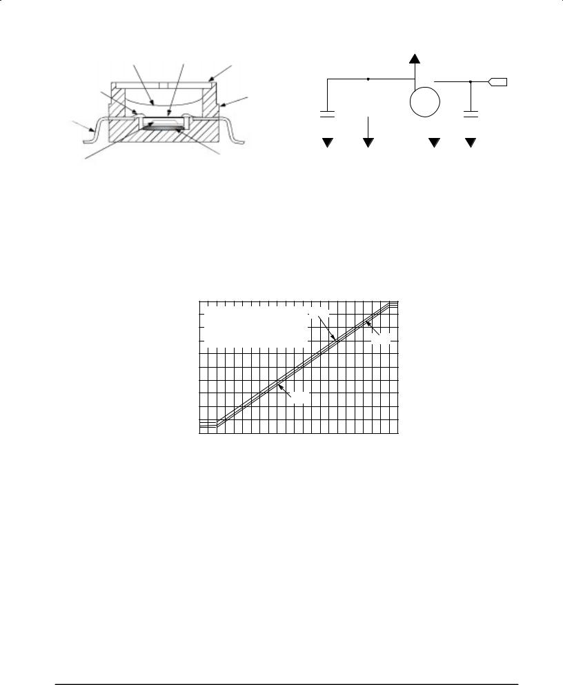
Motorola's MPX4115A/MPXA4115A series sensor integrates on±chip, bipolar op amp circuitry and thin film resistor networks to provide a high output signal and temperature compensation. The small form factor and high reliability of on±chip integration make the Motorola pressure sensor a logical and economical choice for the system designer.
The MPX4115A/MPXA4115A series piezoresistive transducer is a state±of±the±art, monolithic, signal conditioned, silicon pressure sensor. This sensor combines advanced micromachining techniques, thin film metallization, and bipolar semiconductor processing to provide an accurate, high level analog output signal that is proportional to applied pressure.
Figure 1 shows a block diagram of the internal circuitry integrated on a pressure sensor chip.
Features
•1.5% Maximum Error over 0° to 85°C
•Ideally suited for Microprocessor or Microcontroller± Based Systems
•Temperature Compensated from ±40° to +125°C
•Durable Epoxy Unibody Element or Thermoplastic (PPS) Surface Mount Package
Application Examples
•Aviation Altimeters
•Industrial Controls
•Engine Control
•Weather Stations and Weather Reporting Devices
*'
|
|
|
( " ! |
|
|
" '( |
|
' "' " |
|
|
( !$& ()& |
|
" |
|
|
|
|
|
|
||||
|
|
#!$"' ( #" |
|
)" |
*9>= |
||
! "( |
|
|
|
||||
|
|
" |
|
|
& & " |
|
|
|
|
|
|
|
|
||
|
|
|
" '( |
|
|
' ( & ) (&- |
|
|
|
|
|||||
|
|
|
|
|
|
|
|
|
|
|
$"' " & "# #"" (' |
||||
|
|
|
#& '! |
|
#)( " $ |
* |
|
|
" |
|
|
|
|
||
|
|
|
$"' " & "# #"" (' #& |
||||
|
|
|
)" #- |
* |
|
||
Figure 1. Fully Integrated Pressure Sensor
Schematic
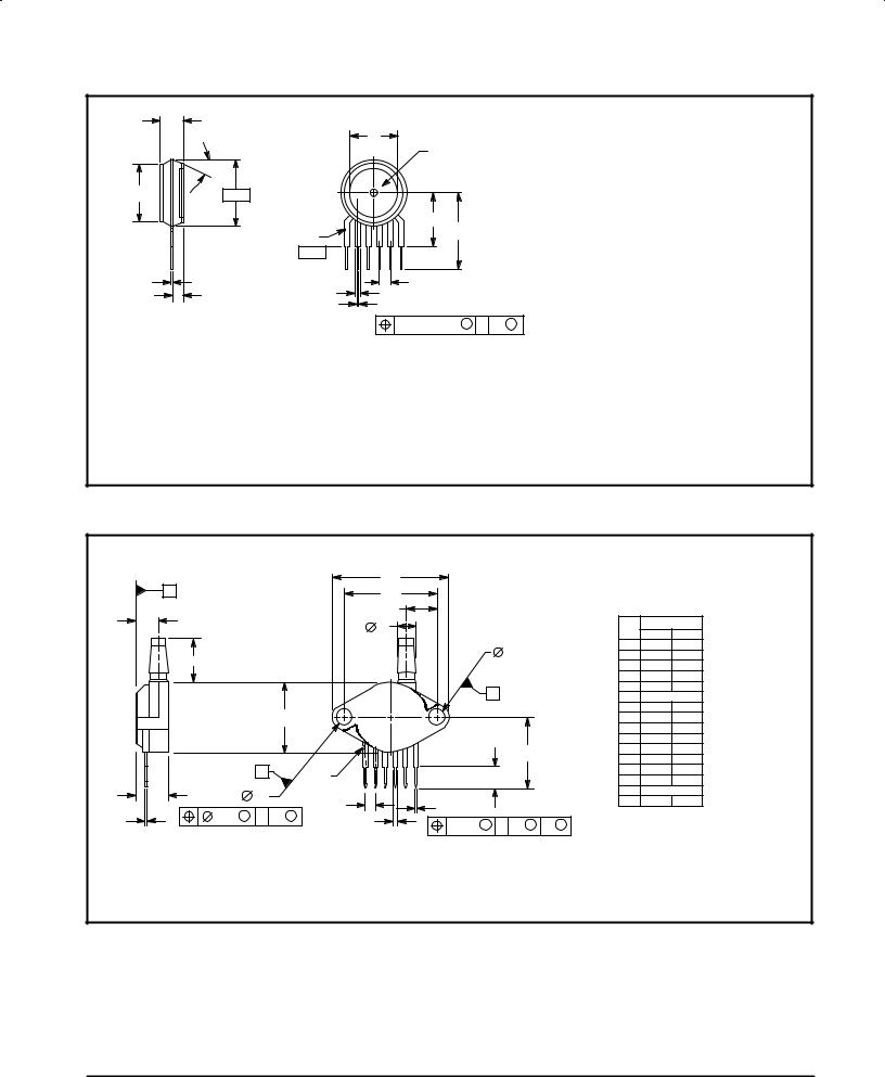
SMALL OUTLINE PACKAGE
MPXA4115A6U
CASE 482
MPXA4115AC6U
CASE 482A
PIN NUMBER
1 |
N/C |
5 |
N/C |
|
|
|
|
2 |
VS |
6 |
N/C |
3 |
Gnd |
7 |
N/C |
|
|
|
|
4 |
Vout |
8 |
N/C |
|
NOTE: Pins 1, 5, 6, 7, and 8 are |
|
internal device connections. Do not |
|
connect to external circuitry or |
REV 4 |
ground. Pin 1 is noted by the notch in |
the lead. |
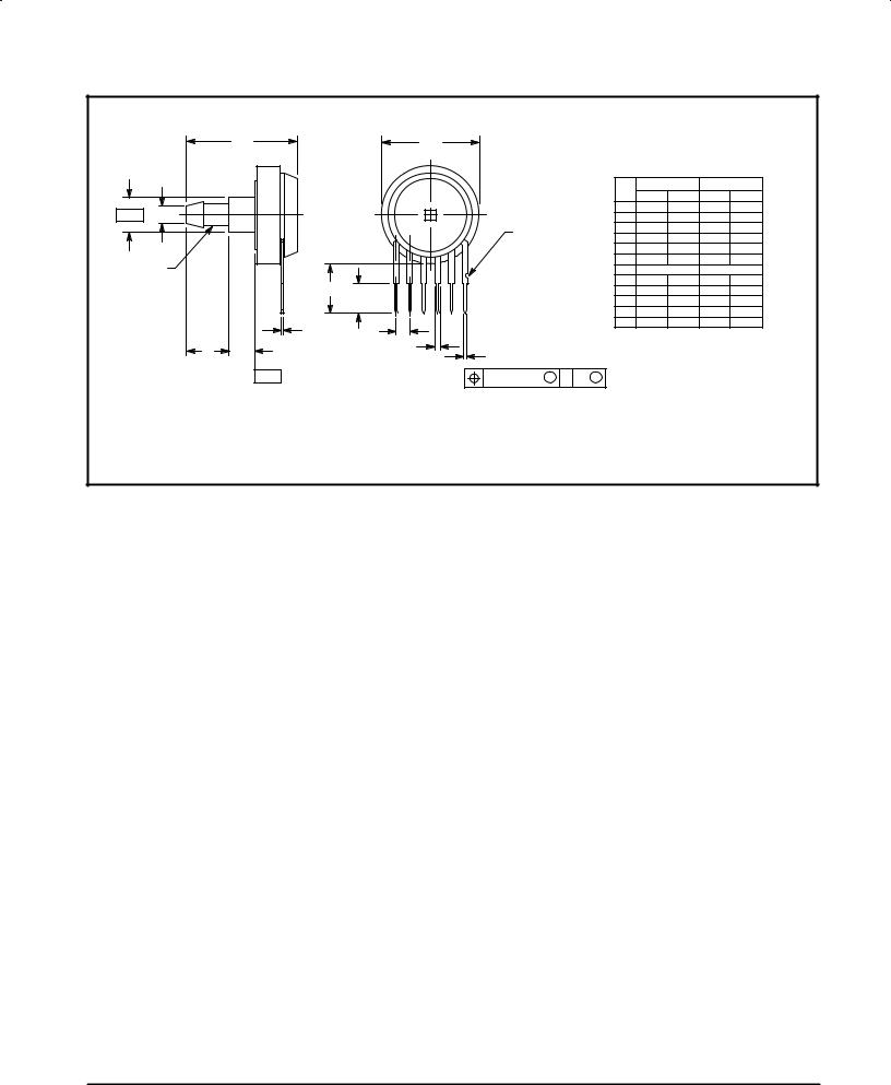
" M M # E E
INTEGRATED
PRESSURE SENSOR
15 to 115 kPa (2.2 to 16.7 psi)
0.2 to 4.8 Volts Output
UNIBODY PACKAGE
MPX4115A
CASE 867
MPX4115AP
CASE 867B
MPX4115AS
CASE 867E
PIN NUMBER
1 |
Vout |
4 |
N/C |
2 |
Gnd |
5 |
N/C |
|
|
|
|
3 |
VS |
6 |
N/C |
NOTE: Pins 4, 5, and 6 are internal device connections. Do not connect to external circuitry or ground. Pin 1 is noted by the notch in the lead.
Motorola Sensor Device Data |
1 |
Motorola, Inc. 2001 |
|

M M |
E E |
|
|
|
|
|
|
|
|
|
|
MAXIMUM RATINGS(NOTE) |
|
|
|
|
|
|
|
|
|
|
|
Parametrics |
|
|
Symbol |
|
|
|
Value |
|
Units |
||
|
|
|
|
|
|
|
|
|
|
|
|
Maximum Pressure (P1 P2) |
|
|
Pmax |
|
|
|
400 |
|
|
kPa |
|
Storage Temperature |
|
|
Tstg |
|
±40° to +125° |
|
|
°C |
|||
Operating Temperature |
|
|
TA |
|
±40° to +125° |
|
|
°C |
|||
NOTE: Exposure beyond the specified limits may cause permanent damage or degradation to the device. |
|
|
|
||||||||
OPERATING CHARACTERISTICS (VS = 5.1 Vdc, TA = 25°C unless otherwise noted, P1 P2. |
Decoupling circuit shown in Figure 3 |
||||||||||
required to meet Electrical Specifications.) |
|
|
|
|
|
|
|
|
|
|
|
|
|
|
|
|
|
|
|
|
|
||
Characteristic |
|
Symbol |
Min |
|
Typ |
|
Max |
|
Unit |
||
|
|
|
|
|
|
|
|
|
|
|
|
Pressure Range |
|
|
POP |
15 |
|
Ð |
|
115 |
|
kPa |
|
Supply Voltage(1) |
|
|
V |
4.85 |
|
5.1 |
|
5.35 |
|
Vdc |
|
|
|
|
S |
|
|
|
|
|
|
|
|
Supply Current |
|
|
Io |
Ð |
|
|
7.0 |
|
10 |
|
mAdc |
Minimum Pressure Offset(2) |
(0 to 85°C) |
|
V |
0.135 |
|
0.204 |
|
0.273 |
|
Vdc |
|
@ VS = 5.1 Volts |
|
|
off |
|
|
|
|
|
|
|
|
|
|
|
|
|
|
|
|
|
|
|
|
|
|
|
|
|
|
|
|
|
|
|
|
Full Scale Output(3) |
(0 to 85°C) |
|
V |
4.725 |
|
4.794 |
|
4.863 |
|
Vdc |
|
@ VS = 5.1 Volts |
|
|
FSO |
|
|
|
|
|
|
|
|
|
|
|
|
|
|
|
|
|
|
|
|
|
|
|
|
|
|
|
|
|
|
|
|
Full Scale Span(4) |
(0 to 85°C) |
|
V |
4.521 |
|
4.590 |
|
4.659 |
|
Vdc |
|
@ VS = 5.1 Volts |
|
|
FSS |
|
|
|
|
|
|
|
|
|
|
|
|
|
|
|
|
|
|
|
|
|
|
|
|
|
|
|
|
|
|
|
|
Accuracy(5) |
(0 to 85°C) |
|
Ð |
Ð |
|
|
Ð |
|
±1.5 |
|
%V |
|
|
|
|
|
|
|
|
|
|
|
FSS |
Sensitivity |
|
|
V/P |
Ð |
|
|
45.9 |
|
Ð |
|
mV/kPa |
|
|
|
|
|
|
|
|
|
|
|
|
Response Time(6) |
|
|
t |
Ð |
|
|
1.0 |
|
Ð |
|
ms |
|
|
|
R |
|
|
|
|
|
|
|
|
Output Source Current at Full Scale Output |
|
Io+ |
Ð |
|
|
0.1 |
|
Ð |
|
mAdc |
|
Warm±Up Time(7) |
|
|
Ð |
Ð |
|
|
20 |
|
Ð |
|
ms |
Offset Stability(8) |
|
|
Ð |
Ð |
|
|
±0.5 |
|
Ð |
|
%V |
|
|
|
|
|
|
|
|
|
|
|
FSS |
NOTES: |
|
|
|
|
|
|
|
|
|
|
|
1.Device is ratiometric within this specified excitation range.
2.Offset (Voff) is defined as the output voltage at the minimum rated pressure.
3.Full Scale Output (VFSO) is defined as the output voltage at the maximum or full rated pressure.
4.Full Scale Span (VFSS) is defined as the algebraic difference between the output voltage at full rated pressure and the output voltage at the minimum rated pressure.
5.Accuracy is the deviation in actual output from nominal output over the entire pressure range and temperature range as a percent of span at 25°C due to all sources of error including the following:
• Linearity: Output deviation from a straight line relationship with pressure over the specified pressure range.
• Temperature Hysteresis: Output deviation at any temperature within the operating temperature range, after the temperature is
|
|
cycled to and from the minimum or maximum operating temperature points, with zero differential |
|
|
pressure applied. |
• |
Pressure Hysteresis: |
Output deviation at any pressure within the specified range, when this pressure is cycled to and from |
|
|
minimum or maximum rated pressure at 25°C. |
• |
TcSpan: |
Output deviation over the temperature range of 0° to 85°C, relative to 25°C. |
• |
TcOffset: |
Output deviation with minimum pressure applied, over the temperature range of 0° to 85°C, relative |
|
|
to 25°C. |
6.Response Time is defined as the time for the incremental change in the output to go from 10% to 90% of its final value when subjected to a specified step change in pressure.
7.Warm±up Time is defined as the time required for the product to meet the specified output voltage after the pressure has been stabilized.
8.Offset Stability is the product's output deviation when subjected to 1000 cycles of Pulsed Pressure, Temperature Cycling with Bias Test.
MECHANICAL CHARACTERISTICS
Characteristics |
Typ |
Unit |
|
|
|
Weight, Basic Element (Case 867) |
4.0 |
grams |
|
|
|
Weight, Small Outline Package (Case 482) |
1.5 |
grams |
|
|
|
2 |
Motorola Sensor Device Data |
|
|
|
|
M |
M |
E E |
|||||
|
|
|
|
|
|
|
|
* |
|
|
|
)# ' #" |
|
'( " '' |
|
|
|
|
|
|
|
|
|
# ( |
|
|
|
|
|
|
|
|
|
||
|
'( |
$ |
|
|
|
|
|
|
|
|
|
|
|
|
|
|
|
|
|
#)($)( |
|||
|
$ |
|
|
|
|
|
|
*9>= |
|||
+ & #" |
( &!#$ '( |
|
|
*< |
|
|
|||||
|
|
|
|
|
|
||||||
|
|
|
|
|
|
|
|
|
|||
|
|
|
|
|
|
|
|
|
|
||
|
|
|
' |
|
|
|
|
$' |
|
|
|
|
|
|
|
|
|
|
|
|
|
||
|
|
|
|
|
|
|
|
|
|
|
|
& ! |
|
|
|
|
|
|
|
|
|
|
|
|
|
|
.0 |
0.0 |
" |
|
0 |
: |
|||
'# )( ! "( |
#" |
|
|
|
|
|
|
|
|
|
|
|
|
|
|
|
|
|
|
|
|||
|
|
|
|
|
|
|
|
|
|
|
|
' * ))! & & " |
|
|
|
|
|
|
|
|
|
|
|
Figure 2. Cross Sectional Diagram SOP |
Figure 3. Recommended power supply decoupling |
||||||||||
|
(not to scale) |
|
|
|
and output filtering. |
|
|
||||
|
|
|
For additional output filtering, please refer to |
||||||||
|
|
|
|
Application Note AN1646. |
|
|
|||||
Figure 2 illustrates the absolute sensing chip in the basic chip carrier (Case 482).
Figure 3 shows the recommended decoupling circuit for interfacing the output of the integrated sensor to the A/D input of a microprocessor or microcontroller. Proper decoupling of the power supply is recommended.
|
.0 |
|
|
|
|
|
|
|
|
|
|
|
|
|
. |
(& "' & )" ( #" |
|
|
! , |
|
|
|
|
|
|||
|
.0 |
*9>= |
|
<* .00 $ .0 ± |
;;9; |
|
|
|
|
|
|
||
|
*' |
|
. |
*0/ |
|
|
|
|
|
|
|
|
|
|
|
|
|
|
|
|
|
|
|
||||
#)($)( *96=< |
3. |
( !$ |
|
0 =9° |
|
|
|
|
(-$ |
|
|
||
3.0 |
|
|
|
|
|
|
|
|
|
|
|
|
|
. |
|
|
|
|
|
|
|
|
|
|
|
|
|
.0 |
|
|
|
|
|
|
|
|
|
|
|
|
|
|
. |
|
|
|
|
|
! " |
|
|
|
|
|
|
|
|
|
|
|
|
|
|
|
|
|
|
||
|
.0 |
|
|
|
|
|
|
|
|
|
|
|
|
|
0. |
|
|
|
|
|
|
|
|
|
|
|
|
|
0 |
0 0 |
30 3 0 0 |
|
0 |
0 0 0 |
00 0 |
0 |
|
0 |
|||
|
|
||||||||||||
|
|
|
|
|
$;1<<>;1 ;12 |
=9 |
<1.610 ?./>>7 |
48 |
5$. |
|
|
|
|
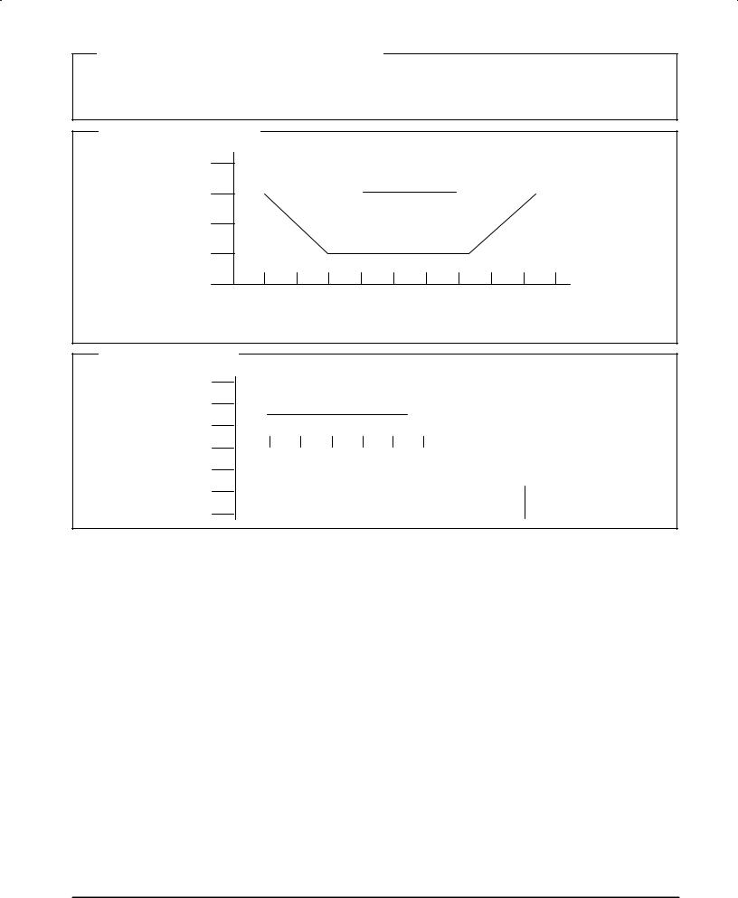
Figure 4. Output versus Absolute Pressure
Figure 4 shows the sensor output signal relative to pressure input. Typical minimum and maximum output curves are shown for operation over 0 to 85°C temperature range. The output will saturate outside of the rated pressure range.
A fluorosilicone gel isolates the die surface and wire bonds from the environment, while allowing the pressure signal to be transmitted to the silicon diaphragm. The
MPX4115A/MPXA4115A series pressure sensor operating characteristics, internal reliability and qualification tests are based on use of dry air as the pressure media. Media other than dry air may have adverse effects on sensor performance and long±term reliability. Contact the factory for information regarding media compatibility in your application.
Motorola Sensor Device Data |
3 |
M M E E
Transfer Function (MPX4115A, MPXA4115A)
Nominal Transfer Value: Vout = VS x (0.009 x P ± 0.095)
± (Pressure Error x Temp. Factor x 0.009 x VS) VS = 5.1 ± 0.25 Vdc
Temperature Error Band
|
|
|
MPX4115A, MPXA4115A Series |
|
|
|
|||||
|
.0 |
|
|
;1.5 |
$948=< |
|
|
|
|
|
|
|
|
|
|
|
|
|
|
|
|||
|
3.0 |
|
|
#$ |
|
'"&!$"! % |
|
|
|
|
|
|
|
|
|
0 |
|
3 |
|
|
|
|
|
|
|
|
|
|
|
|
|
|
|||
(17:1;.=>;1 |
|
|
|
0 |
=9 |
|
|
|
|
|
|
.0 |
|
|
|
|
3 |
|
|
|
|
||
;;9; |
|
|
|
|
|
|
|
||||
|
|
|
|
|
|
|
|
|
|
|
|
./=9; |
|
|
|
|
|
|
|
|
|
|
|
|
.0 |
|
|
|
|
|
|
|
|
|
|
|
0.0 |
|
|
|
|
|
|
|
|
|
|
|
0 |
0 |
0 |
0 |
|
0 |
0 |
0 |
00 |
0 |
0 |
|
|
|
|
|
(17:1;.=>;1 48 ° |
|
|
|
|
||
NOTE: The Temperature Multiplier is a linear response from 0°C to ±40°C and from 85°C to 125°C |
|||||||||||
Pressure Error Band
$;1<<>;1.;;9;5$
3.0
.0
.0
0.0
.0
A .0
A3.0
;;9; 474=< 29; $;1<<>;1
0 |
0 |
0 |
0 |
00 |
0 |
|
$;1<<>;1 48 5$. |
|||
|
|
|
|
|||||||
|
|
|
|
|
|
|
$;1<<>;1 |
|
;;9; !.@ |
|
|
|
|
|
|
|
|
|
|||
|
|
|
|
|
|
|
|
=9 |
5$ |
. ±A . 5$. |
ORDERING INFORMATION Ð UNIBODY PACKAGE
Device Type |
Options |
Case No. |
MPX Series Order No. |
Marking |
|
|
|
|
|
Basic Element |
Absolute, Element Only |
867 |
MPX4115A |
MPX4115A |
|
|
|
|
|
Ported Elements |
Absolute, Ported |
867B |
MPX4115AP |
MPX4115AP |
|
|
|
|
|
|
Absolute, Stove Pipe Port |
867E |
MPX4115AS |
MPX4115A |
|
|
|
|
|
ORDERING INFORMATION Ð SMALL OUTLINE PACKAGE
Device Type |
Options |
Case No. |
MPX Series Order No. |
Packing Options |
Marking |
|
|
|
|
|
|
Basic Element |
Absolute, Element Only |
482 |
MPXA4115A6U |
Rails |
MPXA4115A |
|
|
|
|
|
|
|
Absolute, Element Only |
482 |
MPXA4115A6T1 |
Tape and Reel |
MPXA4115A |
|
|
|
|
|
|
Ported Element |
Absolute, Axial Port |
482A |
MPXA4115AC6U |
Rails |
MPXA4115A |
|
|
|
|
|
|
|
Absolute, Axial Port |
482A |
MPXA4115AC6T1 |
Tape and Reel |
MPXA4115A |
|
|
|
|
|
|
4 |
Motorola Sensor Device Data |

M M E E
INFORMATION FOR USING THE SMALL OUTLINE PACKAGE (CASE 482)
MINIMUM RECOMMENDED FOOTPRINT FOR SURFACE MOUNTED APPLICATIONS
Surface mount board layout is a critical portion of the total design. The footprint for the surface mount packages must be the correct size to ensure proper solder connection interface between the board and the package. With the correct
fottprint, the packages will self±align when subjected to a solder reflow process. It is always recommended to design boards with a solder mask layer to avoid bridging and shorting between solder pads.
0. 00 (-$ ,
|
|
|
|
|
|
|
|
0. 0 |
|
|
|
|
|
. |
||||
|
|
|
|
|
|
|
|
|
|
|
|
|
|
|
|
|
||
|
|
|
|
|
|
|
|
. |
|
|
|
|
|
|
|
|
|
|
0.0 0 (-$ , |
|
|
|
|
|
|
|
|
|
|
|
|
|
|
|
|
|
|
|
|
|
|
|
|
|
|
|
|
|
|
|
|
|
|
|
||
|
|
|
|
|
|
|
|
|
|
|
|
|
|
|
|
|
||
|
|
|
|
|
|
|
|
|
|
|
|
|
|
|
|
|||
|
|
|
|
|
|
|
|
|
|
|
|
|
|
|
|
|||
. |
|
|
|
|
|
|
|
|
|
|
|
|
0.300 |
|
||||
|
|
|
|
|
|
|
|
|
|
|
. |
|||||||
|
|
|
|
|
|
|
|
|
|
|
|
|
|
|
||||
|
|
|
|
|
|
|
|
|
|
|
|
|
|
|||||
|
|
|
|
|
|
|
|
|
|
|
|
|
|
|
|
|
|
|
|
|
|
|
|
|
|
|
|
|
|
|
|
|
|
|
|
|
|
|
|
|
|
|
|
|
|
|
|
|
|
|
|
|
|
|
|
|
|
|
|
|
|
|
|
|
|
|
|
|
|
|
|
|
|
|
|
|
|
|
|
|
|
|
|
0. 00 (-$ , |
|
48/3 |
|
|
|
|
|
|||
|
|
|
|
|
|
|
|
|
|
|
|
|
||||||
|
|
|
|
|
|
|
|
. |
77 |
' |
||||||||
|
|
|
|
|
|
|
|
|||||||||||
|
|
|
|
|
|
|
|
|||||||||||
|
|
|
|
|
|
|
|
|
|
|
|
|
|
|
|
|
||
Figure 5. SOP Footprint (Case 482)
Motorola Sensor Device Data |
5 |

M M E E
SMALL OUTLINE PACKAGE DIMENSIONS
±A±
±B±
S
N
J
 K
K
D 8 PL
|
0. 0.0 0 ! ( ' ' |
G
C |
H |
|
±T± |
PIN 1 IDENTIFIER |
EA |
M |
A E |
"#( '. ! "' #" " " (# & " " $ & "'
- . ! .
. #"( " ! "' #" " .
3.! "' #" " # "#( " ) !# $(&)' #".
. ! , !)! !# $(&)' #" 0. 0.00 .
. * &( |
')& ' (-$ & (. |
|||||
|
|
|
|
|
|
|
|
|
E |
E E |
|
||
|
|
|
A |
|
A |
|
|
A |
0. |
0. |
0. |
0. |
|
|
B |
0. |
0. |
0. |
0. |
|
|
|
0. |
0. 30 |
.3 |
. |
|
|
|
0.03 |
0.0 |
0. |
.0 |
|
|
|
0. 00 ' |
. ' |
|
||
|
|
0.00 |
0.0 0 |
0.0 |
0. |
|
|
|
0.00 |
0.0 |
0. 3 |
0. |
|
|
|
0.0 |
0.0 |
. |
. 0 |
|
|
|
0 |
|
0 |
|
|
|
|
0. 0 |
0. |
0. |
0. |
|
|
|
0. 0 |
0. |
.0 |
. |
|
CASE 482±01
ISSUE O
±A±
N ±B±
S
J
 K
K
D 8 PL
|
0. 0.0 0 ! ( ' ' |
G
W
V
C
|
H |
|
±T± |
PIN 1 IDENTIFIER |
EA |
M |
A E |
"#( '. ! "' #" " " (# & " " $ & "'
- . ! .
. #"( " ! "' #" " .
3.! "' #" " # "#( " ) !# $(&)' #".
. ! , !)! !# $(&)' #" 0. 0.00 .
. * &( |
')& ' (-$ & (. |
|||||
|
|
E |
E E |
|
||
|
|
|
A |
|
A |
|
|
A |
0. |
0. |
0. |
0. |
|
|
B |
0. |
0. |
0. |
0. |
|
|
|
0. 00 |
0. 0 |
. 0 |
3. |
|
|
|
0.03 |
0.0 |
0. |
.0 |
|
|
|
0. 00 ' |
. ' |
|
||
|
|
0.00 |
0.0 0 |
0.0 |
0. |
|
|
|
0.00 |
0.0 |
0. 3 |
0. |
|
|
|
0.0 |
0.0 |
. |
. 0 |
|
|
|
0 |
|
0 |
|
|
|
|
0. |
0. |
. |
.3 |
|
|
|
0. 0 |
0. |
.0 |
. |
|
|
|
0. |
0. |
. |
. |
|
|
|
0. |
0. |
. |
3. |
|
CASE 482A±01
ISSUE A
6 |
Motorola Sensor Device Data |
M M E E
UNIBODY PACKAGE DIMENSIONS
|
C |
|
|
|
|
R |
|
|
|
POSITIVE PRESSURE |
|
|
M |
(P1) |
|
|
|
|
|
B |
±A± |
|
|
|
|
N |
|
|
PIN 1 |
L |
|
|
|
|
|
|
|
|
|
|
EA ±T± |
|
|
|
A E |
|
|
J |
F |
G |
|
S |
D 6 PL |
|
|
|
|
|
|
|
|
0. 3 0.00 ! |
( ! |
|
'(- |
'(- |
'(- |
|
$ " . *#)( |
$ " . #$ " |
$ " |
|
. )" |
. )" |
|
|
3. * |
3. *#)( |
|
|
. * |
. *')$$ - |
|
|
. * |
. *#)( |
|
|
. * , |
. #$ " |
|
"#( '. ! "' #" " " (# & " " $ & "'
|
- . ! . |
|
|
|
|
|
|
0. #"( " |
! "' #" " . |
||||||
. ! "' #" ' " )' * # ( !# |
|||||||
'(#$ |
& " . |
!# |
'(#$ |
& " "#( (# , |
|||
|
.00 0. 30 . |
|
|
|
|
|
|
|
|
|
|
|
|
|
|
|
|
E |
E E |
|
|||
|
|
|
A |
|
|
A |
|
|
A |
0. |
0. 30 |
. |
|
.00 |
|
|
B |
0. |
0. 3 |
3.0 |
|
3. |
|
|
|
0. 00 |
0. 0 |
.0 |
|
. |
|
|
|
0.0 |
0.033 |
0. |
|
0. |
|
|
|
0.0 |
0.0 |
. |
|
. 3 |
|
|
|
0. 00 ' |
. ' |
|
|||
|
|
0.0 |
0.0 |
0.3 |
|
0. 0 |
|
|
|
0. |
0. |
. |
|
. |
|
|
|
30 |
"#! |
30 |
"#! |
|
|
|
|
0. |
0. |
.0 |
|
. |
|
|
|
0. 30 |
0. 0 |
0. |
|
. 3 |
|
|
|
0.0 0 |
0. 0 |
. |
|
. |
|
3. #$ "
. )" 3. *#)(. *')$$ -. *#)(. #$ "
CASE 867±08
ISSUE N
BASIC ELEMENT
|
|
|
|
|
|
A |
"#( ' |
|
|
|
|
|
|
T |
|
|
|
|
|
. ! "' #"' |
& |
" ! ! ( &'. |
|
||||
EA A E |
|
|
|
|
|
U |
. ! "' #"' |
" |
(# & " ' |
$ & |
'! |
||
|
|
|
|
|
|
|
L |
- . ! . |
|
|
|
|
|
|
|
|
|
|
|
|
|
|
|
|
|
|
|
R |
|
|
|
|
|
V |
|
|
E E |
|
|
||
|
|
|
|
|
|
|
|
|
A |
|
|
||
|
|
|
|
|
|
|
|
|
|
||||
|
|
|
|
|
|
|
Q |
A |
.0 |
. |
|
|
|
|
N |
|
|
|
|
|
B |
. |
. |
|
|
||
|
|
|
|
|
|
|
|
. |
. |
|
|
||
|
|
|
|
|
|
|
|
|
|
||||
|
|
|
|
|
|
|
|
|
0. |
0. |
|
|
|
|
|
|
|
|
|
|
Q |
|
. |
. 3 |
|
|
|
|
|
|
|
|
|
|
|
. ' |
|
|
|
||
|
|
|
|
|
B |
|
|
|
0.3 |
0. |
|
|
|
|
|
|
|
|
|
|
|
. |
. |
|
|
||
|
|
|
|
|
|
|
|
|
.3 |
. |
|
|
|
|
|
|
|
|
|
|
0. |
. |
|
|
|||
|
|
|
|
|
|
|
|
|
|
||||
|
|
|
|
|
|
|
|
|
3. |
.0 |
|
|
|
|
|
|
|
|
|
|
K |
|
|
||||
|
|
|
|
|
|
|
|
3. |
.0 |
|
|
||
|
|
|
|
|
|
|
|
|
|
||||
|
|
|
P |
|
|
PIN 1 |
S |
|
. |
.3 |
|
|
|
|
|
|
|
|
|
|
. |
. |
|
|
|||
C |
|
|
P |
|
|
|
|
|
3. ' |
|
|
|
|
|
|
|
|
G |
6X D |
|
. |
. 3 |
|
|
|||
|
0. |
! |
( |
% |
! |
|
|
|
|
|
|
||
|
F |
|
|
|
|
|
|
||||||
J |
0. 3 ! ( $ ' % ' |
'(- |
|
|
|
|
|||||||
|
|
|
|
|
|
|
|
|
|||||
|
|
|
|
|
|
|
|
$ " . * |
|
|
|
|
|
|
|
|
|
|
|
|
|
|
#)( |
|
|
|
|
|
|
|
|
|
|
|
|
|
. )" |
|
|
|
|
|
|
|
|
|
|
|
|
|
3. * |
|
|
|
|
|
|
|
|
|
|
|
|
|
. * |
|
|
|
|
|
|
|
|
|
|
|
|
|
. * |
|
|
|
|
|
|
|
|
|
|
|
CASE 867B±04 |
|
. *, |
|
|
|
|
|
|
|
|
|
|
|
|
|
|
|
|
|
|
|
|
|
|
|
|
|
ISSUEF F |
|
|
|
|
|
|
PRESSURE SIDE PORTED (AP, GP)
Motorola Sensor Device Data |
7 |
M M E E
UNIBODY PACKAGE DIMENSIONSÐCONTINUED
|
|
C |
A |
"#( ' |
|
|
|
|
|
|
. ! "' #" " |
" |
(# & " " $& "' |
||||
|
|
|
|
|||||
|
|
|
|
-. ! |
. |
|
|
|
|
|
|
|
. #"( " ! "' #" " . |
||||
|
|
|
|
|
E |
E E |
||
|
|
|
|
|
|
A |
|
A |
±B± |
V |
|
|
A |
0. 0 |
0. 0 |
. 3 |
. |
|
|
B |
0. |
0. |
. |
. |
||
|
|
|
PIN 1 |
|
0. 0 |
0. 0 |
. |
0. |
|
|
|
|
0.0 |
0.033 |
0. |
0. |
|
|
|
|
|
|||||
|
|
|
|
E |
0. |
0. |
. |
. |
PORT #1 |
|
|
|
0.0 |
0.0 |
. |
. 3 |
|
|
|
|
0. 00 ' |
. ' |
||||
POSITIVE |
|
|
|
0.0 |
0.0 |
0.3 |
0. |
|
PRESSURE |
K |
|
||||||
|
|
0.3 |
0.3 |
. |
. 3 |
|||
|
(P1) |
|
||||||
|
|
S |
|
|
0.300 |
0.3 0 |
. |
. |
|
|
|
|
|
0. 0 |
0. 0 |
. |
. 0 |
|
|
J |
G |
|
0. |
0. |
. |
. 3 |
|
|
|
|
|
|
|
||
|
N |
E |
F |
|
'(- |
|
|
|
|
D 6 PL |
|
$" |
. * |
|
|
||
|
|
|
|
|
|
#)( |
|
|
|
|
±T± |
|
|
|
. )" |
|
|
|
|
0. 3 0.00 ! |
( ! |
|
3. * |
|
||
|
|
|
|
|
|
. * |
|
|
. * . *,
CASE 867E±03
ISSUE D
PRESSURE SIDE PORTED (AS, GS)
8 |
Motorola Sensor Device Data |

M M E E
Motorola reserves the right to make changes without further notice to any products herein. Motorola makes no warranty, representation or guarantee regarding the suitability of its products for any particular purpose, nor does Motorola assume any liability arising out of the application or use of any product or circuit, and specifically disclaims any and all liability, including without limitation consequential or incidental damages. ªTypicalº parameterswhich may be provided in Motorola data sheets and/or specifications can and do vary in different applications and actual performance may vary over time. All operating parameters, including ªTypicalsº must be validated for each customerapplication by customer's technical experts. Motorola does not convey any license under its patent rights nor the rights of others. Motorola products are not designed, intended, or authorized for use as components in systems intended for surgical implant into the body, or other applications intended to support or sustain life, or for any other application in which the failure of the Motorola product could create a situation where personal injury or death may occur. Should Buyer purchase or use Motorola products for any such unintended or unauthorized application,
Buyer shall indemnify and hold Motorola and its officers, employees, subsidiaries, affiliates, and distributors harmless against all claims, costs, damages, and expenses, and reasonable attorney fees arising out of, directly or indirectly, any claim of personal injury or death associated with such unintended or unauthorized use, even if such claim alleges that Motorola was negligent regarding the design or manufacture of the part. Motorola and  are registered trademarks of Motorola, Inc. Motorola, Inc. is an Equal Opportunity/Affirmative Action Employer.
How to reach us: |
|
USA/EUROPE/Locations Not Listed: Motorola Literature Distribution; |
JAPAN: Motorola Japan Ltd.; SPS, Technical Information Center, 3±20±1, |
P.O. Box 5405, Denver, Colorado 80217. 1±303±675±2140 or 1±800±441±2447 |
Minami±Azabu. Minato±ku, Tokyo 106±8573 Japan. 81±3±3440±3569 |
Technical Information Center: 1±800±521±6274 |
ASIA/PACIFIC: Motorola Semiconductors H.K. Ltd.; Silicon Harbour Centre, |
|
2, Dai King Street, Tai Po Industrial Estate, Tai Po, N.T., Hong Kong. |
|
852±26668334 |
HOME PAGE: http://www.motorola.com/semiconductors/ |
|
Motorola Sensor Device Data |
9 |
◊ |
MPX4115A/D |