

Furber S.ARM system-on-chip architecture.2000
.pdfThe JTAG boundary scan test architecture |
229 |
• EXTEST: here the boundary scan register is connected between TDI and TOO and the pin states are captured and controlled by the register. Referring to the state transition diagram in Figure 8.15 on page 228, the pin states are captured in the Capture DR state and shifted out of the register via the TDO pin in the Shift DR state. As the captured data is shifted out, new data is shifted in via the TDI pin, and this data is applied to the boundary scan register outputs (and hence the output pins) in the Update DR state. This instruction exists to support the testing of board-level connectivity.
• IDCODE: here the ID register is connected between TDI and TDO. In the Capture DR state the device ID (a hard-wired identification number giving the manufacturer, part number and version of the part) is copied into the register which is then shifted out in the Shift DR state.
Other public instructions may include:
|
• INTEST: here the boundary scan register is connected between TDI and TDO and |
|
the core logic input and output states are captured and controlled by the register. |
|
Note that the inputs are driven to the complement of the values supplied. Other |
|
wise the operation is similar to EXTEST. This instruction exists to support the |
|
testing of the core logic. |
PCB testing |
The principal goal of the JTAG test circuit is to enable the continuity of tracks and |
|
the connectivity of solder connections on printed circuit boards (PCBs) to be tested. |
|
This has become difficult since the introduction of surface mount packages which |
|
do not require through-holes in the circuit board. Previously 'bed of nails' testers |
|
could contact all the pins on each 1C package from the back of the PCB to check |
|
continuity; surface mount packages typically have the pins closer together and the |
|
tracks accessible only on the component side of the board, making the 'bed of nails' |
|
approach inapplicable. |
|
When the surface mount components have a JTAG test interface, this can be used |
|
(using the EXTEST instruction) to control outputs and observe inputs independently |
|
of the normal function of the chip, so board-level connectivity can readily be checked |
|
from chip to chip. If the board also contains components which do not have a JTAG |
|
interface these will require 'bed of nails' contacts, but these can be used together with |
|
the JTAG interfaces where available to minimize the cost and difficulty of building the |
|
production test equipment. |
VLSI testing |
High-complexity integrated circuits require extensive production testing to identify |
|
faulty devices before they get built into product. A production 1C tester is a very |
|
expensive piece of equipment, and the time each device spends on the tester is an |
|
important factor in its manufacturing cost. Since the JTAG test circuitry operates |
|
through serial access, it is not a high-speed way to apply test vectors to the core |
230 |
Architectural Support for System Development |
logic. Furthermore, it is not possible to apply test vectors through the JTAG port at the normal operating speed of the device to check its performance.
Therefore the JTAG architecture is not a generic solution to all the problems of VLSI production testing. However, it can solve a number of problems:
•The JTAG port can be used for in-circuit functional testing of an 1C (provided that the INTEST instruction is supported).
•It gives good control of the 1C pins for parametric testing (checking the drive of the output buffers, leakage, input thresholds, and so on). This uses only the EXTEST instruction which is required on all JTAG compliant devices.
•It can be used to access internal scan paths to improve the controllability and observability of internal nodes that are hard to access from the pins.
•It can be used to give access to on-chip debug functions with no additional pins and without interfering with the system functions. This is exploited by the ARM EmbeddedlCE debug architecture described briefly below and in detail in Section 8.7 on page 232.
•It offers an approach to the functional testing of macrocell-based designs as described below.
These uses are all in addition to its principal purpose, which is in the production testing of printed circuit boards.
Embedded-ICE |
The ARM debug architecture, described in Section 8.7 on page 232, is based on an |
|
extension of the JTAG test port. The EmbeddedlCE module introduces breakpoint |
|
and watchpoint registers which are accessed as additional data registers using spe- |
|
cial JTAG instructions, and a trace buffer which is similarly accessed. The scan path |
|
around the ARM core macrocell is used to introduce instructions into the ARM |
|
pipeline without interfering with other parts of the system and these instructions can |
|
be used to access and modify the ARM and system state. |
|
The debug architecture gives most of the functionality of a conventional In-Circuit |
|
Emulation system to debug an ARM macrocell on a complex system chip, and since |
|
the JTAG test access port is used to control the debug hardware, no additional pins are |
|
required on the chip. |
Macrocell testing |
A growing trend in the design of complex system chips is to incorporate a number |
|
of complex, pre-designed macrocells, together with some application-specific |
|
custom logic. The ARM processor core is itself one such macrocell; the others may |
|
come from ARM Limited, a semiconductor partner or some third party supplier. |
|
In such cases the designer of the system chip will have limited knowledge of the |
|
macrocells and will depend on the macrocell suppliers for the production test pat- |
|
terns for each macrocell. |
The JTAG boundary scan test architecture |
231 |
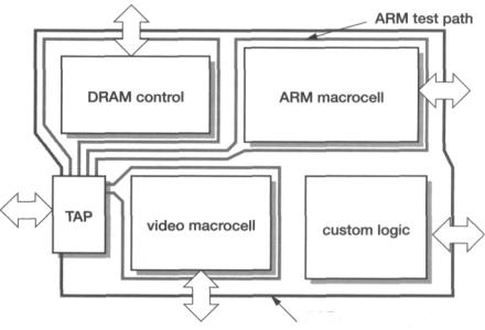
Since the macrocells are buried within the system chip, the designer is faced with the problem of devising a way to apply the supplied test vectors to each of the macro-cells in turn. Test patterns must also be generated for the custom logic part of the design, but the designer is assumed to understand that part of the logic.
There are various approaches to getting the test patterns onto the edges of the macrocells:
•Test modes may be provided which multiplex the signals from each macrocell in turn onto the pins of the system chip.
•An on-chip bus may support direct test access to each macrocell which is attached to it (see Section 8.2 on page 216).
•Each macrocell may have a boundary scan path through which the test patterns may be applied using an extension of the JTAG architecture.
This last approach is illustrated in Figure 8.16. The chip has a peripheral boundary scan path to support the public EXTEST operation and additional paths around each macrocell, designed into the macrocell, for applying functional tests as supplied. The custom logic designed specifically for this chip may have its own scan path or, as shown in the figure, rely on the fact that all its interface signals must intercept one of the existing scan paths.
PCB test scan path
Figure 8.16 A possible JTAG extension for macrocell testing.
232 |
Architectural Support for System Development |
It should be recognized that although perfectly feasible for functional testing, the scan path approach to macrocell testing has the same drawbacks as using the JTAG boundary scan path to test the core logic on a chip. The serial access is much slower than parallel access through the pins and performance testing at speed is not possible.
The most promising production test methodology for macrocell based system chips appears to be to exploit the on-chip bus to give parallel access to the macrocell's periphery (especially where the macrocell has been designed specifically to give good access through this route). Multiplexing is used to give external access to peripheral macrocell signals that are important for performance testing and cannot conveniently be accessed via the on-chip bus, and the JTAG port is used to access other signals and internal state where necessary via scan chains. We have seen this approach as it is supported by ARM's 'Advanced Microcontroller Bus Architecture' (AMBA) which is described in Section 8.2 on page 216; the AMBA testing methodology is described on page 219.
The JTAG system continues to be very important for board-level testing, and can also be used for in-circuit testing of the core logic and to access on-chip debug facilities. It is incorporated into most ARM designs and is an important component of their test and debug methodologies.
8.7The ARM debug architecture
|
Debugging any computer system can be a complex task. There are two basic |
|
approaches to debugging, the simplest being based on watching a system from the |
|
outside using test equipment such as a logic analyser, and the more powerful being |
|
based on viewing a system from the inside with tools that support single stepping, |
|
the setting of breakpoints, and so on. |
Desktop |
When the system to be debugged is a piece of software running on a desktop |
debugging |
machine, all the user interface components are readily available and the debugger |
|
may itself simply be another piece of software running on the same machine. Break- |
|
points are set by replacing an instruction in the object program with a call to the |
|
debugger, remembering the original instruction so that it can be replaced when exe- |
|
cution continues past the breakpoint. |
|
Often compilers have compile-time options to generate extensive debug information |
|
such as symbol tables which the debugger can use to allow the user to debug the pro- |
|
gram from a source-level view, addressing variables by their source names rather than by |
|
their memory address. This 'source-level debugging' is more powerful and requires less |
|
detailed knowledge of the machine environment than object-level debugging. |
|
A common weakness in software debuggers is the lack of a 'watchpoint' facility. A |
|
watchpoint is a memory address which halts execution if it is accessed as a data trans- |
|
fer address. Since many processors have no support for trapping on a particular |
The ARM debug architecture |
233 |
|
address (apart, perhaps, from a memory management page fault, which is rather |
|
coarse for this purpose) this functionality is often omitted. This is a pity, since a very |
|
common source of error in a C program is corrupted data caused by an errant pointer |
|
in some unrelated part of the program, and this can be very hard to track down with- |
|
out a watchpoint facility. |
Embedded |
Debugging becomes significantly more difficult when the target system is embed- |
debugging |
ded. Now there is probably no user interface in the system, so the debugger must |
|
run on a remote host through some sort of communication link to the target. If the |
|
code is in ROM, instructions cannot simply be replaced by calls to the debugger |
|
since the locations are not writeable. |
|
The standard solution here is the In-Circuit Emulator (ICE). The processor in the |
|
target system is removed and replaced by a connection to an emulator. The emulator |
|
may be based around the same processor chip, or a variant with more pins (and more |
|
visibility of its internal state), but it will also incorporate buffers to copy the bus activ- |
|
ity off to a 'trace buffer' (which stores the signals on all the pins in each clock cycle |
|
for some number of cycles) and various hardware resources which can watch for par- |
|
ticular events, such as execution passing through a breakpoint. The trace buffer and |
|
hardware resources are managed by software running on a host desktop system. |
|
When a 'trigger' event occurs, the trace buffer is frozen so the user can observe |
|
activity around the point of interest. The host software will present the trace buffer |
|
data, give a view on the processor and system state and allow it to be modified, and |
|
generally attempt to appear as similar to a debugger in a desktop system as possible. |
Debugging |
The ICE approach depends on the system having an identifiable processor chip which |
processor cores |
can be removed and replaced by the ICE. Clearly, once the processor has become just |
|
one macrocell of many on a complex system chip, this is no longer possible. |
|
Although simulation using software models such as the ARMulator should remove |
|
many of the design bugs before the physical system is built, it is often impossible to |
|
run the full software system under emulation, and it can be difficult to model all the |
|
real-time constraints accurately. Therefore it is likely that some debugging of the com- |
|
plete hardware and software system will be necessary. How can this be achieved? This |
|
is still an area of active research to identify the best overall strategy with acceptable |
|
hardware overhead costs, but considerable progress has been over the last few years in |
|
developing practical approaches, and the rest of this section presents the approach |
|
developed by ARM Limited. |
ARM debug |
To provide debug facilities comparable with those offered by a typical ICE, the user |
hardware |
must be able to set breakpoints and watchpoints (for code running in ROM as well |
|
as RAM), to inspect and modify the processor and system state, to see a trace of |
|
processor activity around the point of interest, and to do all this from the comfort of |
|
a desk-top system with a good user interface. The trace mechanism used in ARM |

234 Architectural Support for System Development
systems is separate from the other debug facilities, and is discussed in Section 8.8 on page 237. In this section we restrict our attention to the breakpoint, watchpoint and state inspection resources.
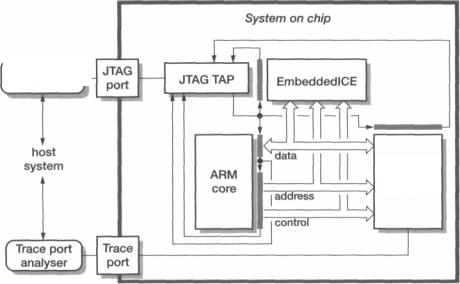
The communication between the target system and the host is achieved by extending the functionality of the JTAG test port. Since the JTAG test pins are included in most designs for board testing, accessing the debug hardware through this port requires no additional dedicated pins, sparing the most precious resource on the chip from further pressure. JTAG scan chains are used to access the breakpoint and watch-point registers and also to force instructions into the processor to access processor and system state.
The breakpoint and watchpoint registers represent a fairly small hardware overhead that can often be accepted on production parts. The host system runs the standard ARM development tools, communicating with the target through a serial port and/or a parallel port. Special protocol conversion hardware sits between the host serial line
|
and the target JTAG port. |
|
In addition to the breakpoint and watchpoint events, it may also be desirable to halt |
|
the processor when a system-level event occurs. The debug architecture includes |
|
external inputs for this purpose. |
|
The on-chip cell containing these facilities is called the EmbeddedlCE module. |
Embedded-ICE |
The EmbeddedlCE module consists of two watchpoint registers and control and |
|
status registers. The watchpoint registers can halt the ARM core when the address, |
|
data and control signals match the value programmed into the watchpoint register. |
|
Since the comparison is performed under a mask, either watchpoint register can be |
|
configured to operate as a breakpoint register capable of halting the processor when |
|
an instruction in either ROM or RAM is executed. |
|
The comparison and mask logic is illustrated in Figure 8.17. |
Figure 8.17 EmbeddedlCE signal comparison logic.
The ARM debug architecture |
235 |
Chaining |
|
Each watchpoint can look for a particular combination of values on the ARM |
||
|
|
address bus, data bus, trans, ope, mo?[l:0] and r/w control signals, and if either |
||
|
|
combination is matched the processor is stopped. Alternatively, the two watchpoints |
||
|
|
may be chained to halt the processor when the second watchpoint is matched only |
||
|
|
after the first has previously been matched. |
||
Registers |
|
EmbeddedlCE registers are programmed via the JTAG test port, using a dedicated |
||
|
|
scan chain. The scan chain is 38 bits long, with 32 data bits, 5 address bits and a r/w |
||
|
|
bit which controls whether the register is read or written. The address bits specify |
||
|
|
the particular register following the mapping detailed in Table 8.1. |
||
|
|
Table 8.1 |
EmbeddedlCE register mapping. |
|
|
|
|
|
|
Address |
Width |
Function |
|
|
|
|
|
|
|
00000 |
3 |
Debug control |
|
|
00001 |
5 |
Debug status |
|
|
00100 |
6 |
Debug comms control register |
|
|
00101 |
32 |
Debug comms data register |
|
|
01000 |
32 |
Watchpoint 0 address value |
|
|
01001 |
32 |
Watchpoint 0 address mask |
|
|
01010 |
32 |
Watchpoint 0 data value |
|
|
01011 |
32 |
Watchpoint 0 data mask |
|
|
01100 |
9 |
Watchpoint 0 control value |
|
|
01101 |
8 |
Watchpoint 0 control mask |
|
|
10000 |
32 |
Watchpoint 1 address value |
|
|
10001 |
32 |
Watchpoint 1 address mask |
|
|
10010 |
32 |
Watchpoint 1 data value |
|
|
10011 |
32 |
Watchpoint 1 data mask |
|
|
10100 |
9 |
Watchpoint 1 control value |
|
|
10101 |
8 |
Watchpoint 1 control mask |
|
|
|
|
|
|
|
|
|
The use of the JTAG scan chain is illustrated in Figure 8.18 on page 236. The read |
||
|
|
or write takes place when the TAP controller enters the 'update DR' state (see |
||
|
|
Figure 8.15 on page 228). |
||
Accessing state |
The EmbeddedlCE module allows a program to be halted at specific points, but it does |
|||
|
|
not directly allow the processor or system state to be inspected or modified. This is |
||
|
|
achieved via further scan paths which are also accessed through the JTAG port. |
||

236 |
Architectural Support for System Development |
|
breakpoint Figure 8.18 |
|
EmbeddedlCE register read and write structure. |
|
The mechanism employed to access the processor state is to halt the processor, then |
|
to force an instruction such as a store multiple of all the registers into the processor's |
|
instruction queue.Then clocks are applied to the processor, again via the scan chain, |
|
causing it to write the registers out through its data port. Each register is collected by |
|
the scan chain and shifted out. |
|
System state is harder to glean, since there may be system locations that cannot be |
|
read at the very low speeds that the scan path can generate. Here the processor is pre- |
|
loaded with a suitable instruction, then allowed to access the system location at system |
Debug comms |
speed. This transfers the required system state into a processor register, whereupon it |
may be passed to the external debugger through the JTAG port as described above. |
|
|
In additions to the breakpoint and watchpoint registers, the EmbeddedlCE module |
|
also includes a debug comms port whereby the software running on the target |
|
system can communicate with the host. The software in the target system sees the |
|
comms port as a 6-bit control register and 32-bit data read and write registers which |
Debugging |
are accessed using MRC and MCR instructions to coprocessor 14. The host sees |
these registers in the EmbeddedlCE register map as shown in Table 8.1 on page 235. |
|
|
An ARM-based system chip which includes the EmbeddedlCE module connects to |
|
a host computer through the JTAG port and a protocol converter. This configuration |
|
supports the normal breakpoint, watchpoint and processor and system state access |
|
that the programmer is accustomed to using for native or ICE-based debugging (in |
|
addition to the comms port described above), and with suitable host software gives a |
|
full source-level debugging capability with low hardware overhead. |
|
The only facility that is missing is the ability to trace code in real time. This is the |
|
function of the Embedded Trace Macrocell described in the next section. |

Embedded Trace |
237 |
8.8Embedded Trace
Trace compression
Real-time debug
When debugging real-time systems it is often difficult to debug the application software without the capability of observing its operation in real time. The breakpoint and watchpoint facilities offered by the EmbeddedlCE macrocell are insufficient for this purpose as using them causes the processor to deviate from its normal execution sequence, destroying the temporal behaviour of the software.
What is required is an ability to observe the processor operating at full speed by generating a trace of its address, data and control bus activity as the program executes. The problem is that this represents a huge data bandwidth - an ARM processor running at 100 MHz generates over 1 Gbyte/s of interface information. Getting this information off the chip would require so many pins that it would be uneconomic to include the capability on production devices, so special development devices would be needed, adversely affecting the costs of developing a new system-on-chip application.
The solution adopted by ARM Limited is to reduce the interface bandwidth using intelligent trace compression techniques. For example:
•Most ARM addresses are sequential, so it is not necessary to send every address off chip. Instead, the sequential information can be sent on most cycles and the full address only when a branch is taken.
•If there is off-chip logic which has access to the code which is running on the processor, it will know when the processor is executing a branch instruction and where the target of the branch is. The only information which must be sent off chip is whether or not the branch is taken.
•Fuller address information is now required only when the branch target is not known, such as in a subroutine return or jump table instruction. Even here, only those low-order address bits that change need be issued.
•The address information is now very bursty. A first-in-first-out (FIFO) buffer can be used to smooth the data rate so that the necessary address information can be transmitted in 4-, 8- or 16-bit packets at a steadier rate.
Using a number of techniques similar along these lines, the ARM Embedded Trace Macrocell can compress the trace information to the extent necessary to allow it to be communicated off chip through 9, 13 or 21 pins depending on the configuration. These pins could be used for other purposes when trace output is not required.
A complete real-time debug solution is as shown in Figure 8.19 on page 238. The EmbeddedlCE unit supports breakpoint and watchpoint functionality, and communication channels between the host and target software. The Embedded Trace Macrocell compresses the processor's interface information and sends it off chip through the Trace port. The JTAG port is used to control both units. The external EmbeddedlCE
238 |
Architectural Support for System Development |
EmbeddedlCE|
controller
Embedded trace macrocell
Figure 8.19 Real-time debug system organization.
controller is used to connect the host system to the JTAG port, and the external Trace Port Analyser interfaces the host system to the Trace port. The host may connect to both the trace port analyser and the EmbeddedlCE controller via a network.
The user has control of the breakpoint and watchpoint settings and various trace functions. All the application software may be traced, or just particular routines. Trigger conditions can be specified, and the trace can be collected before or after the trigger or with the trigger in the centre of the trace. Data accesses can be selected to be included in the trace or not, and the trace may collect just the address of the data access, or just the data itself, or both.
Embedded trace As noted above, the Embedded Trace Macrocell may be synthesized in several dif- options ferent configurations allowing the functionality of the unit to be traded off against
cost (measured in terms of the numbers of gates and pins used).
•The minimal system requires 5 pins to issue pipeline information and 4 pins to issue data (in addition to the 5-pin JTAG interface). This is sufficient for execution tracing, but will only support very limited data tracing and has restricted triggering and filter ing capabilities. A 9-byte FIFO is used to smooth the data transfer rate, and the hard ware cost of this implementation is approximately 15 Kgates.
•A maximal system uses 5 pins to issue pipeline information and 16 pins to issue data (again, in addition to the 5-pin JTAG interface). It is capable of tracing the flow of execution and all but the very-worst-case data activity. A 40-byte FIFO is used to smooth the data flow, and the hardware cost is approximately 50 Kgates.