

Bologna / 04_TCAD_laboratory_pn_junction_GBB_20150223H1655
.pdfOutline
•Review of basic properties of the diode
•Sentaurus Workbench setup (SWB)
•Implementation of Input files
–Sentaurus Structure Editor (SDE) command file
–Sentaurus Device (SDevice)
•command file
•parameter file
•Run the simulation
Post-processing of results
G. Betti Beneventi 31
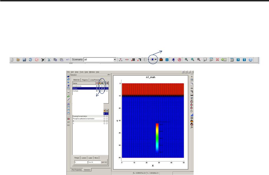
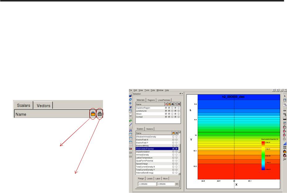
Output of the simulation: Svisual (1)
• Geometry, doping & mesh
Select the first SDE real node (n1) then click on the “eye” button at the top of the bar Sentaurus Visual (Select File) n1_msh.tdr new S-Visual instance Ok
• Explore the Svisual tool functionalities to obtain the visualization of doping and mesh on the whole geometry..
to activate for visualization of the numerical mesh
G. Betti Beneventi 32

Output of the simulation: Svisual (2)
•Visualization of a cut-line of the doping concentration (i.e. doping concentration profile at a given x)
•Select on the right-hand side toolbar Precision Cut Create Cuts
precision cut tool
indicate which coordinate is constant in the
cut indicate which is the selected coordinate
G. Betti Beneventi 33
Output of the simulation: Svisual (3)
•Window Plot_n1_msh (deselect) Selection
BoronActiveConcentration To Left Y-Axis PhosphorusActiveConcentration To Left Y-Axis
•Select on right hand side bar, logY, logY2
•Click on the legend, then Legend properties Position Lower Right
•Double click on the graph on the left Y axis set Min. 1e14 and Max. 1e18. Do the same for the right Y2 axis
•Select Title/Scale, in title attributes of Y axis Concentration enter
•Select Title/Scale, in title attributes of Y2 axis Concentration enter
•Selection Curves DopingConcentration Delete
•BoronActiveConcentration Curve Properties Shape
Solid increase up to 4 Markers CircleF, write 10 in the cell
•Close the data window (click on Data on the left hand-side toolbar)
•Close the property window (click on Prop on the left hand-side toolbar)
•Export the figure: ExportPlot (the camera) n1_msh_doping_X=25μm save (by default files are exported in the .png format)
•Use the Probe (the speedometer) to determine the location of the junction, verify that the junction is located around X ~ 10
right-hand side toolbar
left-hand side toolbar
G. Betti Beneventi 34
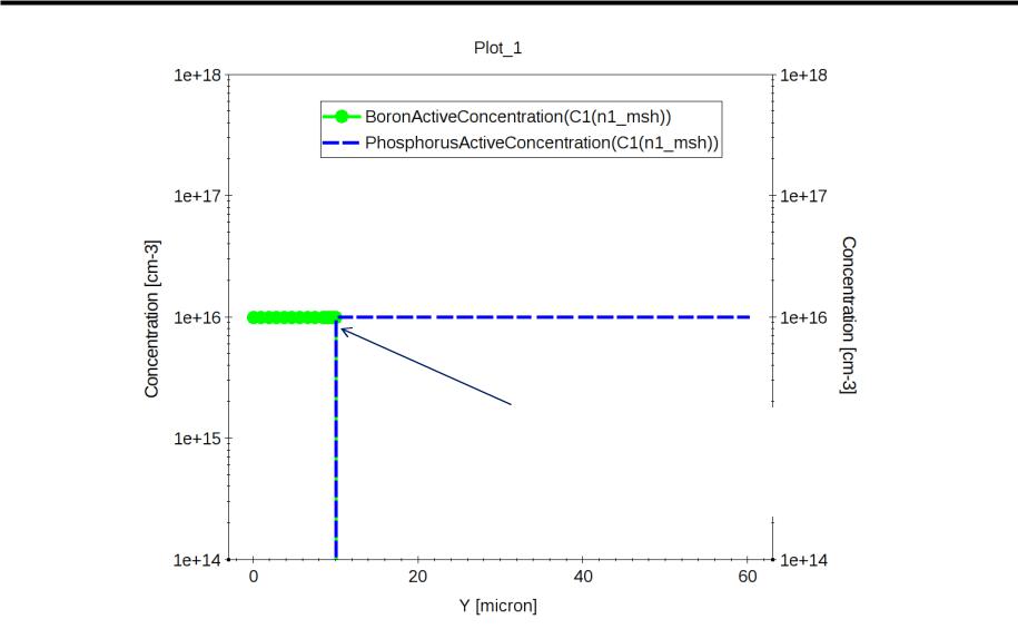
Saved image file
x~10 determines the junction line (in brown in the simulator), that is, where the sign of doping changes
G. Betti Beneventi 35
Post-processing: Svisual (4)
•Band diagram at equilibrium (1)
•Select the first real node of Sdevice (n2) click on the “eye” button Sentaurus Svisual
(Select File …) n2_000000_des.tdr new S-Visual instance Ok
N.B. n2_000000_des.tdr is the Equilibrium solution see the correspondence in the Sdevice command file, i.e. first “coupled” command
To find out the correspondence, reconsider for example the first quasistationary ramp: quasistationary (InitialStep = 0.010 MaxStep = 0.005 MinStep=0.005
Goal {name= "p_contact" voltage = @V_start@} plot { range=(0, 1) intervals=1 }
)
{coupled {poisson electron hole} }
normalized units: it means that from V_start=0 to V_start=V_start/V_start there is 1 interval, so the files will be saved as (note that V_start is negative)
n2_000001_des.tdr
|
|
|
n2_000000_des.tdr |
|
|
range= 1 interval |
|
|
|
|
V |
|
|
|
|
V_start |
0 |
||
|
|
|
G. Betti Beneventi 36 |
Post-processing: Svisual (5)
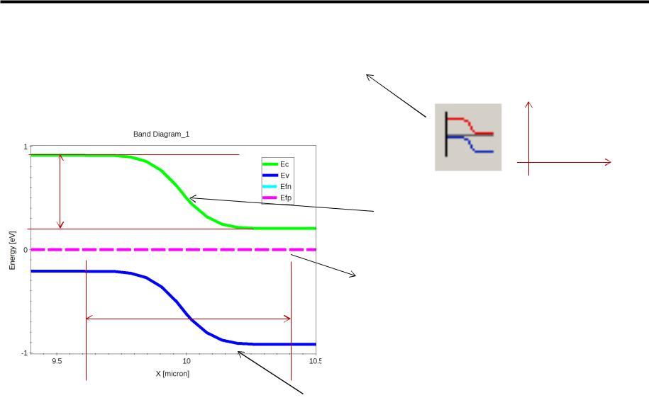
•Band diagram at equilibrium (2)
•Select Precision cuts Create cuts Plot Band Diagram ok
•Window select Plot_n2_000000_des
•Zoom on the plot to magnify the junction
0.9
P N
0 = ∆ ~0.7
0.2
Energy
length
as we calculated with the compact formula
there is a single flat quasi Fermi level because we are at equilibrium
junction width (region where bands are bended), about 800nm wrt to a total length of 60 μm! (Wp+Wn)
G. Betti Beneventi 37
Post-processing: Svisual (6)
•Electrostatic Potential
•Window select Plot_n2_000000_des
•Window select Plot_1
•Open the data window (click on Data on the left hand-side toolbar)
•Click on ElectrostaticPotential, enable Contour Bands and Contour
Lines and zoom at the junction see that electrostatic potential gradient is practically zero on the x axis the device could have been further approximated to 1D !!
Scalars Contour Bands
Scalars Contour Lines
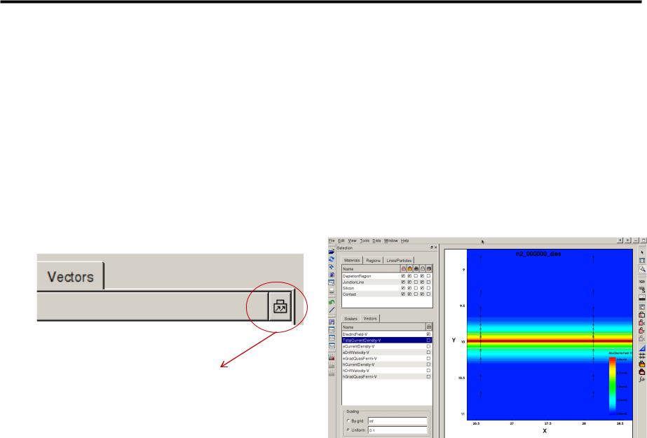
Post-processing: Svisual (7)
•Electric Field
•See how the Contour Lines of the Electrostatic Potential are much
closer around the junction line since the Contour Lines are traced for a fixed potential difference it means that the electric field is higher at the junction
•Deselect Contour Bands and Contour Lines in the Electrostatic Potential
•Select Contour Bands in Abs(ElectricField-V) then switch to Vector and
select Contour Lines in ElectricField-V. Then zoom-out.
•Note how the electric field is parallel to the Y axis, and how it goes from n-region
(doped acceptor, positive charge) to p-region (doped donors, negative charge)
Vectors Contour Lines
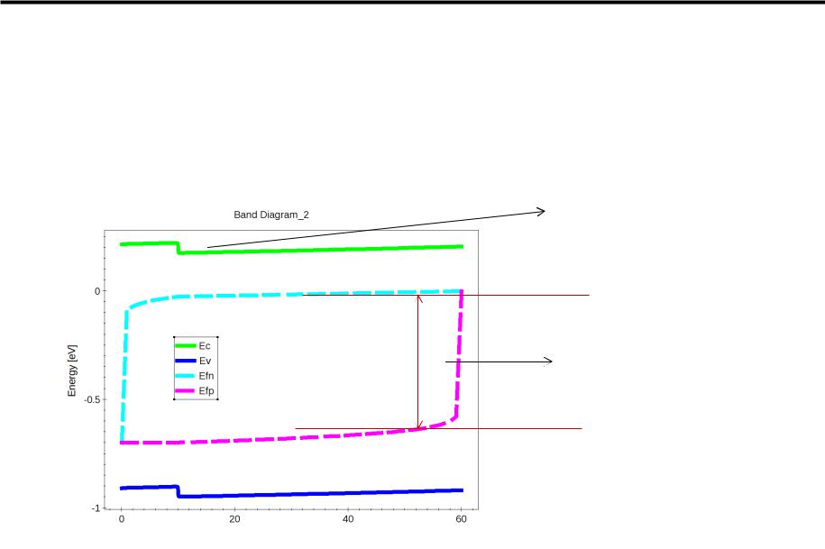
Post-processing: Svisual (8)
•Band diagram in forward bias (at threshold)
•Close the Svisual instance
•Select the first real node of Sdevice (n2) click on the “eye” button Sentaurus Svisual
(Select File …) n2_000009_des.tdr new S-Visual instance Ok
• Select Precision cuts Create cuts Plot Band Diagram Ok
•Window deselect Plot_n2_000009_des
~0.7
bands are almost flat: no barrier anymore
energetic gap between Fermi levels (in eV) equals the applied voltage
> injection of excess carriers compared
to equilibrium
Y [micron] |
G. Betti Beneventi 40 |
|