

Bologna / 04_TCAD_laboratory_pn_junction_GBB_20150223H1655
.pdfPost-processing: Svisual (9)
•Minority carries in forward bias
•Curves select all
curves Delete Data hDensity To Left Y-Axis eDensity To Left Y- Axis
•AcceptorConcentration To Left Y-Axis DonorConcentration To Left Y-Axis
•Zoom around 10 value on x- axis and check the profiles to be approximately linear (no physical model for generation recombination has been implemented!)
linear scale
junction width
excess carrier with respect to equilibrium
G. Betti Beneventi 41
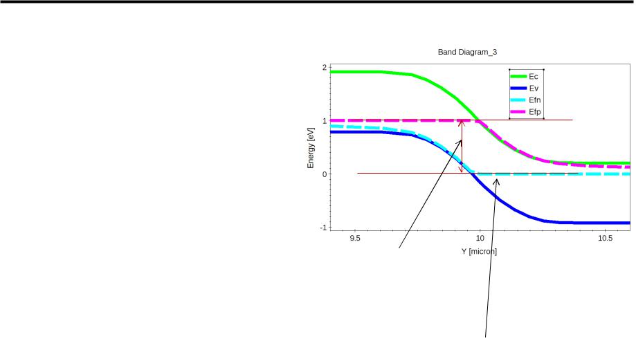
Post-processing: Svisual (10)
•Band diagram in reverse bias
•Close Svisual instance
•How to choose the right .tdr file? Check
on the Sdevice command file! The first quasistationary ramp is about decreasing p_contact to goal, and the number of intervals is 1 (i.e. two .tdr files are saved: n2_000000_des.tdr and n2_000001_des.tdr). Thus, we are interested in the n2_000001_des.tdr node, which has V=V_start=-1V.
•Select the first real node of Sdevice (n2)
click on the “eye” button
Sentaurus Svisual (Select File
…) n2_000001_des.tdr new S- Visual instance Ok
•Select Precision cuts Create
cuts Plot Band Diagram ok
•Window select Plot_n2_000001_des
•Zoom on the plot to magnify the junction
∆V~ − 1 equal to the applied voltage
The fact that near the junction < indicates the presence of a depletion region
G. Betti Beneventi 42
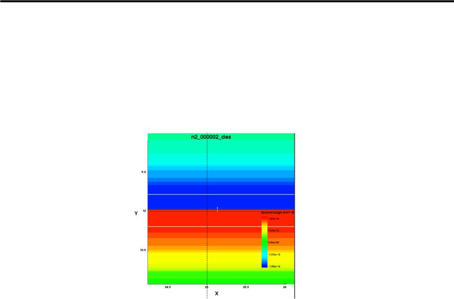
Post-processing: Svisual (11)
•Depletion region and junction line
•Window Plot_1 Window Plot_n2_000001_des
•Zoom at the junction Select SpaceCharge in the Scalars field
•Probe inside the region delimited by the white lines (indicating the electrostatic space-charge
region) around the brown line (indicating the junction line):
•Check that eDensity and hDensity values are well below the doping values, that is check that , , (definition of electrostatic space-charge region)
G. Betti Beneventi 43

Post-processing: Svisual (12)
•Minority carries in reverse bias
•Curves select all curves
Delete Data hDensity To Left
Y-Axis eDensity To Right Y-
Axis
•AcceptorConcentration To Left Y-Axis DonorConcentration To Right Y-Axis
•Zoom around 10 and check the profiles to be
approximately linear (no physical model for generation recombination has been
implemented!) junction width
•N.B. The fact that the profiles do not appear identically symmetrical is only due to different mesh discretization
carrier depletion with respect to equilibrium
G. Betti Beneventi 44

Electrical characteristics: Inspect (1)
•Diode IV characteristics
•Click on n2 node click on “eye” button Inspect (All Files…)
•Select n2_des.plt dataset p_contact OuterVoltage To X-Axis TotalCurrent To Left-Y-Axis
•Set logY on the upper toolbar to plot the characteristics in log scale
deviation from  exponential
behavior due to series resistance
threshold voltage ~ 0.7 V
G. Betti Beneventi 45
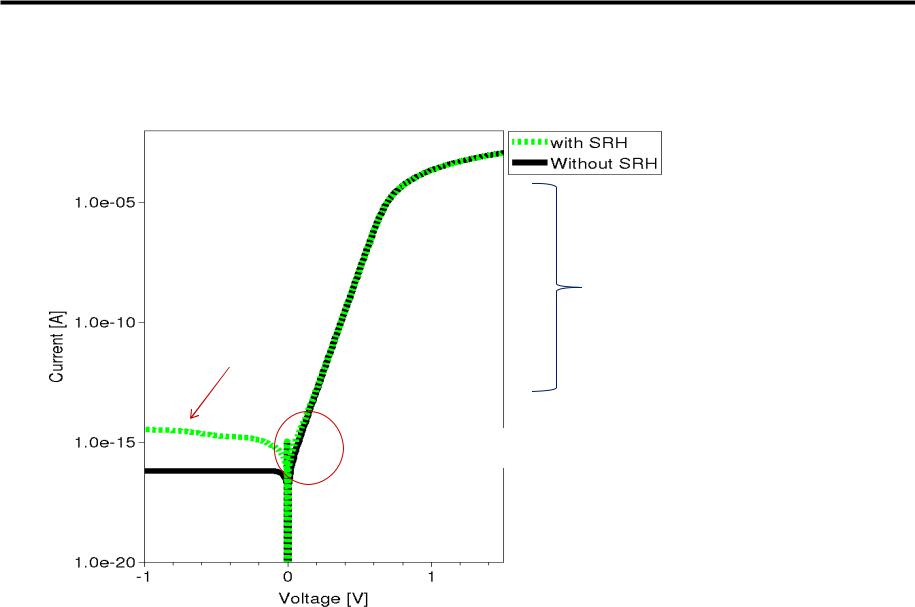
Electrical characteristics: Inspect (2)
•Diode IV characteristics with SRH
•File Load Dataset go to Project folder select n37_des.plt dataset p_contact OuterVoltage To X-Axis TotalCurrent To Left-Y-Axis
|
diffusion |
|
higher |
||
dominates this |
||
reverse |
||
region: |
||
current |
||
curves are |
||
owing to SRH |
||
superimposed |
||
|
||
|
different slope
G. Betti Beneventi 46

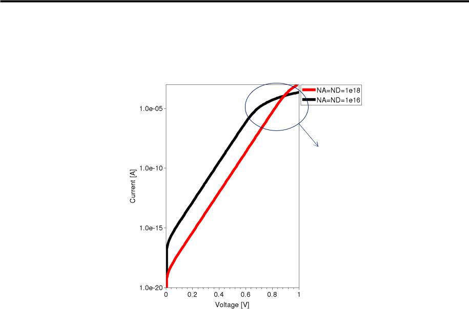
Electrical characteristics: Inspect (3)
• What if we increase doping? Threshold increases
|
|
|
|
|
|
= 1016 |
× 1016 |
→ ~697 mV |
|
0 |
= ln |
|
|
|
|
0 |
|||
|
|
|
|
|
|
|
|
||
|
|
|
|
|
|
|
|
||
|
|
2 |
|
|
|
= 1018 |
× 1018 |
→ ~937 mV |
|
|
|
|
|
|
|||||
|
|
|
|
|
|
|
|
0 |
|
•Click on n2,n34 nodes holding CTRL
click on “eye” button Inspect (All Files…)
•Select all dataset holding CTRL
p_contact OuterVoltage To
X-Axis TotalCurrent To
Left-Y-Axis
G. Betti Beneventi 47
Electrical characteristics: Inspect (4)
• … but slope does not change: check it out by plotting Y in log-scale. Slope is always the same and it is equal to 60 mV/decade of current. This is related to the physics of charge injection (thermionic emission) in non-degenerate semiconductors.
deviation from theoretical
slope due to series resistance effect
G. Betti Beneventi 48
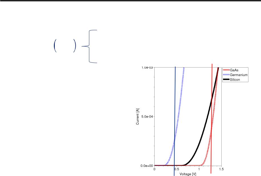
Electrical characteristics: Inspect (5)
• Germanium and GaAs diodes
|
|
|
|
= 1.79 106 |
→ ~1.287 mV (GaAs) |
0 |
= ln |
|
|
0 |
|
|
|
|
|
||
|
|
|
|
||
|
|
2 |
|
|
|
|
|
|
|
= 2.4 1013 |
→ ~434 mV (Ge) |
|
|
|
|
||
|
|
|
|
|
0 |
•Click on n2,n19,n28 nodes holding
CTRL click on “eye” button
Inspect (All Files…)
•Select all dataset holding CTRL p_contact OuterVoltage To X-Axis TotalCurrent To Left-Y-Axis
49
Uniform doping: resistors (1)
•From SWB interface double click on SDE symbol Input Files Edit…
•Go to p-region doping section
•Modify (sdedr:define-constant-profile "p-doping-profile" BoronActiveConcentration @p_doping@) into(sdedr:define-constant- profile "p-doping-profile" "@p_doping_type@" @p_doping@)
•From SWB interface, click on p_doping right click Add Parameter
p_doping_type Default value BoronActiveConcentration ok
•Click on n29 node PhosphorusActiveConcentration
•Click on n30 CTRL-R Yes Run
•Click on n34 CTRL-R Run
no junction anymore, uniform n-doping
G. Betti Beneventi 50