

XILINX SOLUTIONS
SPARTAN-IIE FPGAS
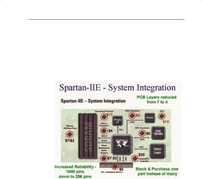
The Spartan-IIE (1.8V core) family of FPGAs offers some of the most advanced FPGA technologies available today, including programmable support for multiple I/O standards (including LVDS, LVPECL, and HSTL); on-chip block RAM; and digital delay lock loops for both chip-level and board-level clock management.
In addition, Spartan-IIE devices provide superior value by eliminating the need for many simple ASSPs such as phase lock loops, FIFOs, I/O translators, and system bus drivers that in the past have been necessary to complete a system design.
FIGURE 2-7: SPARTAN-IIE SYSTEM INTEGRATION
Xilinx • 31

PROGRAMMABLE LOGIC DESIGN: QUICK START HANDBOOK • CHAPTER 2
FIGURE 2-8: SPARTAN-IIE ARCHITECTURE
SPARTAN-IIE ARCHITECTURAL FEATURES
Spartan-IIE devices leverage the basic feature set of the Virtex-E architecture to offer outstanding value. The basic CLB structure contains distributed RAM and performs basic logic functions.
Four DLLs are used for clock management and can perform clock de-skew, clock multiplication, and clock division. Clock de-skew can be done on an external (board level) or internal (chip level) basis.
The block memory blocks are 4 Kb each and can be configured from 1 to 16 bits wide. Each of the two independent ports can be configured independently for width.
The SelectIO feature allows many different I/O standards to be implemented in the areas of chip-to-chip, chip-to-memory, and chip-to-backplane interfaces.
Xilinx • 32
XILINX SOLUTIONS
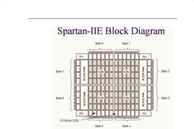
FIGURE 2-9: SPARTAN-IIE BLOCK DIAGRAM
The Spartan-IIE family of FPGAs is implemented with a regular, flexible, programmable architecture of CLBs, surrounded by a perimeter of programmable IOBs, interconnected by a powerful hierarchy of versatile routing resources.
The architecture also provides advanced functions such as block RAM and clock control blocks.
Xilinx • 33

PROGRAMMABLE LOGIC DESIGN: QUICK START HANDBOOK • CHAPTER 2
FIGURE 2-10: SPARTAN-IIE INPUT/OUTPUT BLOCK
The Spartan-IIE IOB features inputs and outputs that support 19 I/O signalling standards, including LVDS, BLVDS, LVPECL, LVCMOS, HSTL, SSTL, and GTL.
These high-speed inputs and outputs are capable of supporting various state-of-the-art memory and bus interfaces. Three IOB registers function either as edge-triggered D-type flip-flops or as level-sensitive latches. Each IOB has a CLK shared by the three registers and independent CE signals for each register.
In addition to the CLK and CE control signals, the three registers share a set/reset. For each register, you can independently configure this signal as a synchronous set, a synchronous reset, an asynchronous preset, or an asynchronous clear.
Xilinx • 34

XILINX SOLUTIONS
FIGURE 2-11: SPARTAN-IIE BANKING OF I/O STANDARDS
Some of the I/O standards require VCCO and/or VREF voltages. These voltages are connected externally to device pins that serve groups of IOBs, called banks.
Consequently, restrictions exist about which I/O standards can be combined within a given bank. Eight I/O banks result from separating each edge of the FPGA into two banks. Each bank has multiple VCCO pins, all of which must be connected to the same voltage. This voltage is determined by the output standards in use.
Logic Cells
The basic building block of the Spartan-IIE CLB is the logic cell. A logic cell includes a four-input function generator, carry logic, and a storage element.
The output from the function generator in each logic cell drives both the CLB output and the D input of the flip-flop. Each Spartan-IIE CLB contains four logic cells, organized in two similar slices.
In addition to the four basic logic cells, the Spartan-IIE CLB contains logic that combines function generators to provide functions of five or six inputs. Consequently, when estimating the number of system gates provided by a given device, each CLB counts as 4.5 logic cells.
Xilinx • 35
PROGRAMMABLE LOGIC DESIGN: QUICK START HANDBOOK • CHAPTER 2
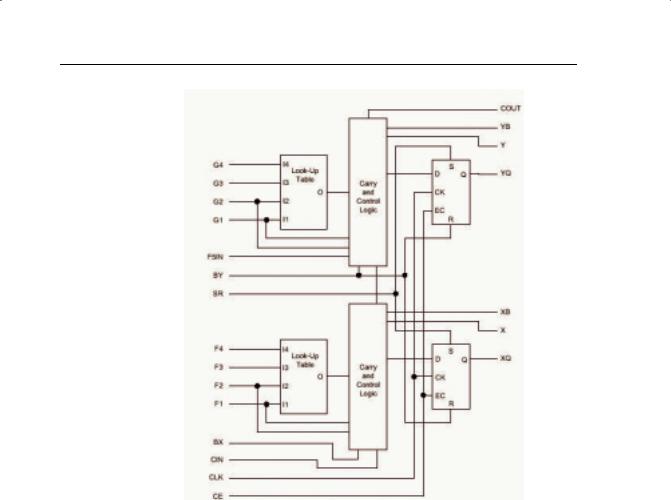
FIGURE 2-12: SPARTAN-IIE LOGIC CELL
Spartan-IIE function generators are implemented as 4-input LUTs. In addition to operating as a function generator, each LUT can provide a 16 x 1-bit synchronous RAM.
Furthermore, two LUTs within a slice can be combined to create a 16 x 2-bit or 32 x 1-bit synchronous RAM, or a 16 x 1-bit dual-port synchronous RAM.
The Spartan-IIE LUT can also provide a 16-bit shift register that is ideal for capturing high-speed or burst-mode data. This SRL16 mode can increase the effective number of flip-flops by a factor of 16.
Adding flip-flops enables fast pipelining, which is ideal for DSP applications. The storage elements in the Spartan-IIE slice can be configured either as edge-triggered D-type flip-flops or as level-sensitive latches.
Xilinx • 36
XILINX SOLUTIONS
Block RAM
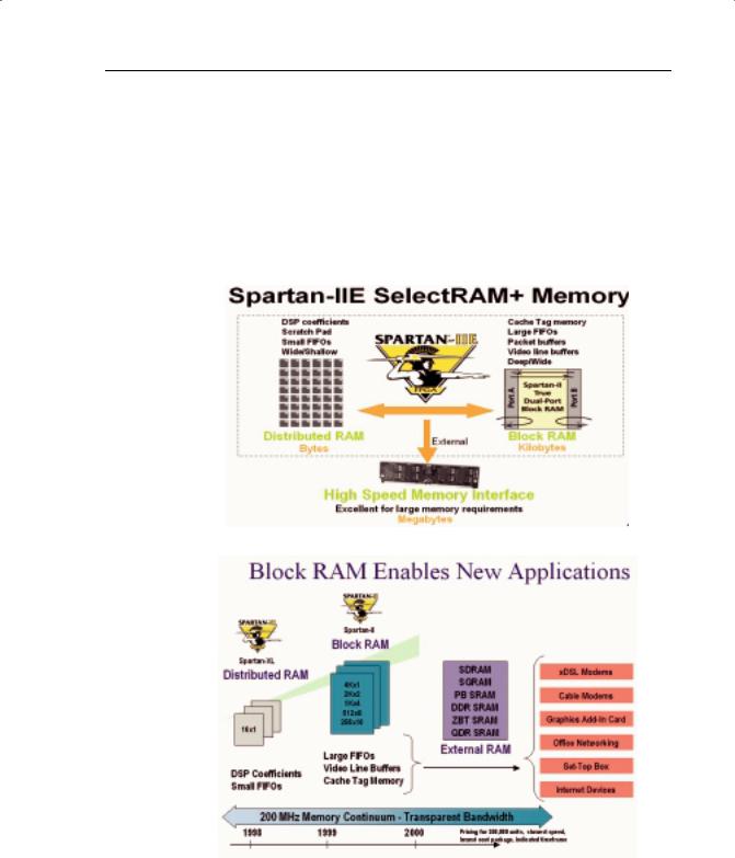
Spartan-IIE FPGAs incorporate several large block SelectRAM+™ memories. These complement the distributed SelectRAM+ resources that provide shallow RAM structures implemented in CLBs.
Block SelectRAM+ memory blocks are organized in columns. All Spartan-II devices contain two such columns, one along each vertical edge. These columns extend the full height of the chip.
Each memory block is four CLBs high, and consequently, a Spartan-IIE device eight CLBs high will contain two memory blocks per column, and a total of four blocks.
FIGURE 2-13: SPARTAN-IIE ON-CHIP MEMORY
FIGURE 2-14: BLOCK RAM APPLICATIONS
Xilinx • 37

PROGRAMMABLE LOGIC DESIGN: QUICK START HANDBOOK • CHAPTER 2
Delay-Locked Loop
Associated with each global clock input buffer is a fully digital DLL that can eliminate skew between the clock input pad and internal clock input pins throughout the device.
Each DLL drives two global clock networks. The DLL monitors the input clock and the distributed clock, and automatically adjusts a clock delay element. Additional delay is introduced such that clock edges reach internal flip-flops exactly one clock period after they arrive at the input.
This closed-loop system effectively eliminates clock-distribution delay by ensuring that clock edges arrive at internal flip-flops in synch with clock edges arriving at the input.
FIGURE 2-15: SPARTAN-IIE CLOCK MANAGEMENT
Xilinx • 38
XILINX SOLUTIONS
FIGURE 2-16: SPARTAN FAMILY COMPARISON
Configuration
Configuration is the process by which the FPGA is programmed with a configuration file generated by the Xilinx development system. Spartan-IIE devices support both serial configuration, using the master/slave serial and JTAG modes, as well as byte-wide configuration employing the slave parallel mode.
Xilinx • 39
PROGRAMMABLE LOGIC DESIGN: QUICK START HANDBOOK • CHAPTER 2
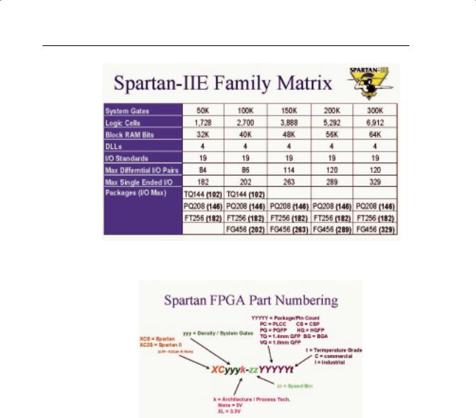
FIGURE 2-17: SPARTAN-IIE FAMILY OVERVIEW
FIGURE 2-18: SPARTAN FPGA PART NUMBERING GUIDE
Xilinx • 40