

Микропроцессорная техника Сторожок / Datasheet.hk_dspic33fj32mc204_1234824
.pdfdsPIC33FJ32MC202/204 and dsPIC33FJ16MC304
FIGURE 14-2: 2-CHANNEL PWM MODULE BLOCK DIAGRAM (PWM2)
PWM2CON1 |
PWM Enable and Mode SFRs |
|
|
|
|
|
PWM2CON2 |
|
|
|
|
|
|
P2DTCON1 |
|
|
|
|
|
|
|
Dead-Time Control SFRs |
|
|
|
|
|
P2DTCON2 |
|
|
|
|
|
|
P2FLTACON |
Fault Pin Control SFRs |
|
|
|
|
|
P2OVDCON |
PWM Manual |
|
|
|
|
|
Control SFR |
|
|
|
|
||
|
|
|
|
|
||
|
PWM Generator # 1 |
|
|
|
|
|
|
P2DC1Buffer |
|
|
|
|
|
Bus |
P2DC1 |
|
|
|
|
|
bit Data |
|
|
|
|
||
Comparator |
Channel 1 Dead-Time |
PWM2H1 |
||||
16- |
||||||
|
|
Generator and |
PWM2L1 |
|||
|
|
|
Override Logic |
|||
P2TMR |
|
|
|
|
|
|
|
|
|
|
Output |
|
|
Comparator |
|
|
|
Driver |
|
|
|
|
|
|
Block |
|
|
P2TPER |
|
|
|
|
|
|
P2TPER Buffer |
|
|
|
|
|
|
P2TCON |
|
|
|
|
FLTA2 |
|
Comparator |
|
Special Event |
Special Event Trigger |
|
||
|
|
Postscaler |
|
|
||
|
SEVTDIR |
|
|
|
||
|
|
|
|
|
||
P2SECMP |
PTDIR |
|
|
|
|
|
PWM Time Base |
|
|
|
|
|
|
♥ 2007 Microchip Technology Inc.
Preliminary
DS70283B-page 149

dsPIC33FJ32MC202/204 and dsPIC33FJ16MC304
14.3PWM Time Base
The PWM time base is provided by a 15-bit timer with a prescaler and postscaler. The time base is accessible via the PXTMR SFR. PXTMR<15> is a read-only status bit, PTDIR, that indicates the present count direction of the PWM time base.
•If PTDIR is cleared, PXTMR is counting upward.
•If PTDIR is set, PxTMR is counting downward.
The PWM time base is configured using the PxTCON SFR. The time base is enabled or disabled by setting or clearing the PTEN bit in the PXTCON SFR. PXTMR is not cleared when the PTEN bit is cleared in software.
The PXTPER SFR sets the counting period for PXTMR. The user application must write a 15-bit value to PXTPER<14:0>. When the value in PXTMR<14:0> matches the value in PXTPER<14:0>, the time base will either reset to ‘0’ or reverse the count direction on the next occurring clock cycle. The action taken depends on the operating mode of the time base.
Note: If the PWM Period register is set to 0x0000, the timer will stop counting and the interrupt and Special Event Trigger will not be generated, even if the special event value is also 0x0000. The module will not update the PWM Period register if it is already at 0x0000; therefore, the user application must disable the module in to update the PWM Period register.
The PWM time base can be configured for four different modes of operation:
•Free-Running mode
•Single-Shot mode
•Continuous Up/Down Count mode
•Continuous Up/Down Count mode with interrupts for double updates
These four modes are selected by the PTMOD<1:0> bits in the PXTCON SFR. The Up/Down Count modes support center-aligned PWM generation. The SingleShot mode allows the PWM module to support pulse control of certain Electronically Commutative Motors (ECMs).
The interrupt signals generated by the PWM time base depend on the mode selection bits (PTMOD<1:0>) and the postscaler bits (PTOPS<3:0>) in the PXTCON SFR.
14.3.1FREE-RUNNING MODE
In Free-Running mode, the PWM time base counts upwards until the value in the PWM Time Base Period register (PXTPER) is matched. The PXTMR register is reset on the following input clock edge, and the time base will continue to count upward as long as the PTEN bit remains set.
When the PWM time base is in the Free-Running mode (PTMOD<1:0> = 00), an interrupt event is generated each time a match with the PXTPER register occurs and the PXTMR register is reset to zero. The postscaler selection bits can be used in this mode of the timer to reduce the frequency of interrupt events.
14.3.2SINGLE-SHOT MODE
In Single-Shot mode, the PWM time base begins counting upward when the PTEN bit is set. When the value in the PXTMR register matches the PXTPER register, the PXTMR register will be reset on the following input clock edge, and the PTEN bit will be cleared by the hardware to halt the time base.
When the PWM time base is in Single-Shot mode (PTMOD<1:0> = 01), an interrupt event is generated when a match with the PXTPER register occurs. The PxTMR register is reset to zero on the following input clock edge and the PTEN bit is cleared. The postscaler selection bits have no effect in this mode of the timer.
14.3.3CONTINUOUS UP/DOWN COUNT MODES
In Continuous Up/Down Count modes, the PWM time base counts upward until the value in the PXTPER register is matched. The timer will begin counting downwards on the following input clock edge. The PTDIR bit in the PXTMR SFR is read-only and indicates the counting direction. The PTDIR bit is set when the timer counts downward.
In the Up/Down Count mode (PTMOD<1:0> = 10), an interrupt event is generated each time the value of the PXTMR register becomes zero and the PWM time base begins to count upward. The postscaler selection bits can be used in this mode of the timer to reduce the frequency of interrupt events.
DS70283B-page 150 |
Preliminary |
♥ 2007 Microchip Technology Inc. |

dsPIC33FJ32MC202/204 and dsPIC33FJ16MC304
14.3.4DOUBLE UPDATE MODE
In Double Update mode (PTMOD<1:0> = 11), an interrupt event is generated each time the PXTMR register is equal to zero, as well as each time a period match occurs. The postscaler selection bits have no effect in this mode of the timer.
Double Update mode provides two additional functions:
•The control loop bandwidth is doubled because the PWM duty cycles can be updated twice per period.
•Asymmetrical center-aligned PWM waveforms can be generated, which can be useful for minimizing output waveform distortion in certain motor control applications.
Note: Programming a value of 0x0001 in the PWM Period register could generate a continuous interrupt pulse and must be avoided.
14.3.5PWM TIME BASE PRESCALER
The input clock to PXTMR (FOSC/4) has prescaler options of 1:1, 1:4, 1:16 or 1:64, selected by control bits PTCKPS<1:0> in the PXTCON SFR. The prescaler counter is cleared when any of the following occur:
•A write to the PXTMR register
•A write to the PXTCON register
•Any device Reset
The PXTMR register is not cleared when PXTCON is written.
14.3.6PWM TIME BASE POSTSCALER
The match output of PXTMR can optionally be postscaled through a 4-bit postscaler (which gives a 1:1 to 1:16 scaling).
The postscaler counter is cleared when any of the following occur:
•A write to the PXTMR register
•A write to the PXTCON register
•Any device Reset
The PXTMR register is not cleared when PXTCON is written.
14.4PWM Period
PXTPER is a 15-bit register used to set the counting period for the PWM time base. PXTPER is a doublebuffered register. The PXTPER buffer contents are loaded into the PXTPER register at the following instants:
•Free-Running and Single-Shot modes: When the PXTMR register is reset to zero after a match with the PxTPER register.
•Up/Down Count modes: When the PxTMR register is zero.
The value held in the PxTPER buffer is automatically loaded into the PxTPER register when the PWM time base is disabled (PTEN = 0).
The PWM period can be determined using Equation 14-1:
EQUATION 14-1: PWM PERIOD
TPWM = TCY • (PXTPER + 1) • (PXTMR Prescale Value)
If the PWM time base is configured for one of the Up/ Down Count modes, the PWM period will be twice the value provided by Equation 14-1.
The maximum resolution (in bits) for a given device oscillator and PWM frequency can be determined using Equation 14-2:
EQUATION 14-2: PWM RESOLUTION
Resolution =
log (2 • TPWM/TCY)
log (2)
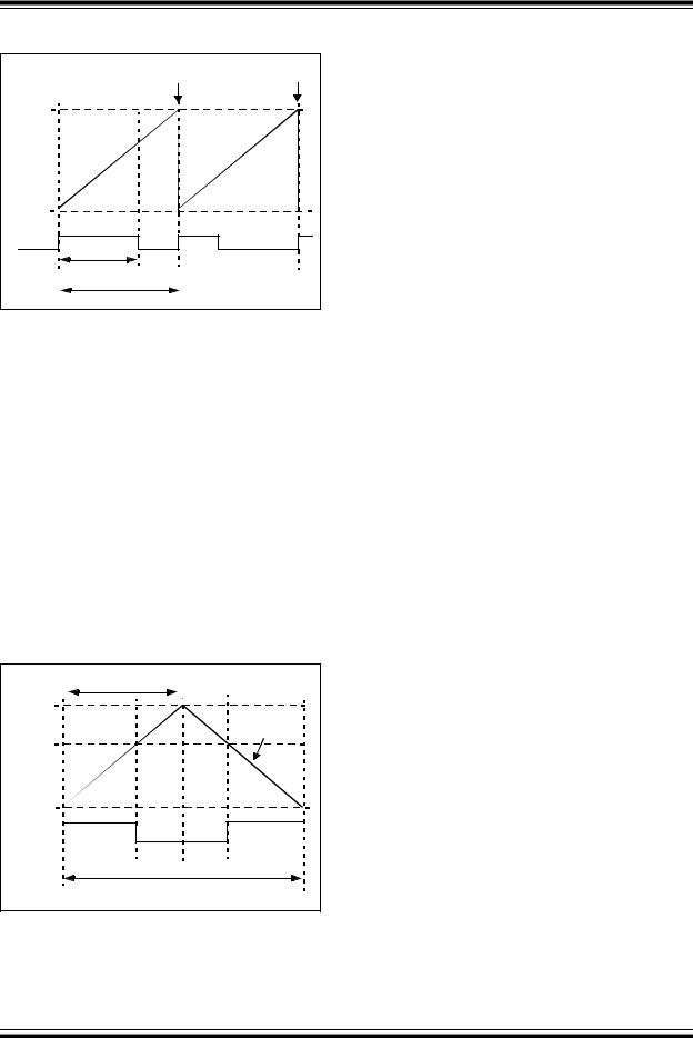
14.5Edge-Aligned PWM
Edge-aligned PWM signals are produced by the module when the PWM time base is in Free-Running or SingleShot mode. For edge-aligned PWM outputs, the output has a period specified by the value in PxTPER and a duty cycle specified by the appropriate Duty Cycle register (see Figure 14-3). The PWM output is driven active at the beginning of the period (PxTMR = 0) and is driven inactive when the value in the Duty Cycle register matches PxTMR.
If the value in a particular Duty Cycle register is zero, the output on the corresponding PWM pin is inactive for the entire PWM period. In addition, the output on the PWM pin is active for the entire PWM period if the value in the Duty Cycle register is greater than the value held in the PxTPER register.
♥ 2007 Microchip Technology Inc.
Preliminary
DS70283B-page 151
dsPIC33FJ32MC202/204 and dsPIC33FJ16MC304
FIGURE 14-3: EDGE-ALIGNED PWM
New Duty Cycle Latched |
PxTPER |
PXTMR |
Value |
0 |
Duty Cycle |
Period |
14.6Center-Aligned PWM
Center-aligned PWM signals are produced by the module when the PWM time base is configured in an Up/Down Count mode (see Figure 14-4).
The PWM compare output is driven to the active state when the value of the Duty Cycle register matches the value of PxTMR and the PWM time base is counting downward (PTDIR = 1). The PWM compare output is driven to the inactive state when the PWM time base is counting upward (PTDIR = 0) and the value in the PxTMR register matches the duty cycle value.
If the value in a particular Duty Cycle register is zero, the output on the corresponding PWM pin is inactive for the entire PWM period. In addition, the output on the PWM pin is active for the entire PWM period if the value in the Duty Cycle register is equal to the value held in the PxTPER register.
FIGURE 14-4: CENTER-ALIGNED PWM
|
Period/2 |
PxTPER |
PTMR |
|
|
Duty |
Value |
|
|
Cycle |
|
0 |
|
|
Period |
14.7PWM Duty Cycle Comparison Units
Three 16-bit Special Function Registers (PxDC1, PxDC2, PxDC3) are used to specify duty cycle values for the PWM module.
The value in each Duty Cycle register determines the amount of time that the PWM output is active. The Duty Cycle registers are 16 bits wide. The Least Significant bit (LSb) of a Duty Cycle register determines whether the PWM edge occurs in the beginning. Thus the PWM resolution is effectively doubled.
14.7.1DUTY CYCLE REGISTER BUFFERS
The three PWM Duty Cycle registers are doublebuffered to allow glitchless updates of the PWM outputs. For each duty cycle, there is a Duty Cycle register that is accessible by the user application and a second Duty Cycle register that holds the actual compare value used in the present PWM period.
For edge-aligned PWM output, a new duty cycle value will be updated whenever a match with the PxTPER register occurs and PxTMR is reset. The contents of the duty cycle buffers are automatically loaded into the Duty Cycle registers when the PWM time base is disabled (PTEN = 0) and the UDIS bit is cleared in PWMxCON2.
When the PWM time base is in the Up/Down Count mode, new duty cycle values are updated when the value of the PxTMR register is zero, and the PWM time base begins to count upward. The contents of the duty cycle buffers are automatically loaded into the Duty Cycle registers when the PWM time base is disabled (PTEN = 0).
When the PWM time base is in the Up/Down Count mode with double updates, new duty cycle values are updated when the value of the PxTMR register is zero, and when the value of the PxTMR register matches the value in the PxTPER register. The contents of the duty cycle buffers are automatically loaded into the Duty Cycle registers when the PWM time base is disabled (PTEN = 0).
DS70283B-page 152 |
Preliminary |
♥ 2007 Microchip Technology Inc. |

dsPIC33FJ32MC202/204 and dsPIC33FJ16MC304
14.7.2DUTY CYCLE IMMEDIATE UPDATES
When the Immediate Update Enable bit is set (IUE = 1), any write to the Duty Cycle registers updates the new duty cycle value immediately. This feature gives programmers the option to allow immediate updates of the active PWM Duty Cycle registers instead of waiting for the end of the current time base period. Duty cycle update effects are as follows:
•If the PWM output is active at the time the new duty cycle is written and the new duty cycle is less than the current time base value, the PWM pulse width will be shortened.
•If the PWM output is active at the time the new duty cycle is written and the new duty cycle is greater than the current time base value, the PWM pulse width will be lengthened.
•If the PWM output is inactive at the time the new duty cycle is written and the new duty cycle is greater than the current time base value, the PWM output will become active immediately and will remain active for the new written duty cycle value.
System stability is improved in closed-loop servo applications by reducing the delay between system observation and the issuance of system corrective commands when immediate updates are enabled (IUE = 1).
14.8Complementary PWM Operation
In the Complementary mode of operation, each pair of PWM outputs is obtained by a complementary PWM signal. A dead time can be inserted during device switching, when both outputs are inactive for a short period (refer to Section 14.9 “Dead-Time Generators”).
In Complementary mode, the duty cycle comparison units are assigned to the PWM outputs as follows:
•PxDC1 register controls PWM1H/PWM1L outputs
•PxDC2 register controls PWM2H/PWM2L outputs
•PxDC3 register controls PWM3H/PWM3L outputs
Complementary mode is selected for each PWM I/O pin pair by clearing the appropriate PMODx bit in the PWMxCON1 SFR. The PWM I/O pins are set to Complementary mode by default upon a device Reset.
14.9Dead-Time Generators
Dead-time generation can be provided when any of the PWM I/O pin pairs are operating in Complementary Output mode. The PWM outputs use push-pull drive circuits. Power output devices cannot switch instantaneously, so some amount of time must be provided between the turn-off event of one PWM output in a complementary pair and the turn-on event of the other transistor.
The PWM module allows two different dead times to be programmed. These two dead times can be used in one of two methods to increase user flexibility:
•The PWM output signals can be optimized for different turn-off times in the high side and low side transistors in a complementary pair of transistors. The first dead time is inserted between the turn-off event of the lower transistor of the complementary pair and the turn-on event of the upper transistor. The second dead time is inserted between the turn-off event of the upper transistor and the turn-on event of the lower transistor.
•The two dead times can be assigned to individual PWM I/O pin pairs. This operating mode allows the PWM module to drive different transistor/load combinations with each complementary PWM I/O pin pair.
14.9.1DEAD-TIME GENERATORS
Each complementary output pair for the PWM module has a 6-bit down counter that is used to produce the dead-time insertion. As shown in Figure 14-5, each dead-time unit has a rising and falling edge detector connected to the duty cycle comparison output.
FIGURE 14-5: DEAD-TIME TIMING DIAGRAM
Duty Cycle Generator
PWMxH
PWMxL
|
|
|
|
|
|
|
|
|
|
|
|
|
|
|
|
|
|
|
|
|
|
|
|
|
|
|
|
|
|
|
|
|
|
|
|
|
|
|
|
|
|
|
|
Time Selected by DTSxA bit (A or B) |
|
Time Selected by DTSxI bit (A or B) |
||||||||
♥ 2007 Microchip Technology Inc.
Preliminary
DS70283B-page 153

dsPIC33FJ32MC202/204 and dsPIC33FJ16MC304
14.9.2DEAD-TIME ASSIGNMENT
The PxDTCON2 SFR contains control bits that allow the dead times to be assigned to each of the complementary outputs. Table 14-1 summarizes the function of each dead-time selection control bit.
TABLE 14-1: DEAD-TIME SELECTION BITS
Bit |
Function |
|
|
|
|
DTS1A |
Selects PWMxL1/PWMxH1 active edge |
|
dead time. |
DTS1I |
Selects PWMxL1/PWMxH1 inactive edge |
|
dead time. |
DTS2A |
Selects PWMxL2/PWMxH2 active edge |
|
dead time. |
DTS2I |
Selects PWMxL2/PWMxH2 inactive edge |
|
dead time. |
DTS3A |
Selects PWMxL3/PWMxH3 active edge |
|
dead time. |
DTS3I |
Selects PWMxL3/PWMxH3 inactive edge |
|
dead time. |
14.9.3DEAD-TIME RANGES
The amount of dead time provided by each dead-time unit is selected by specifying the input clock prescaler value and a 6-bit unsigned value. The amount of dead time provided by each unit can be set independently.
Four input clock prescaler selections have been provided to allow a suitable range of dead times, based on the device operating frequency. The clock prescaler option can be selected independently for each of the two dead-time values. The dead-time clock prescaler values are selected using the DTAPS<1:0> and DTBPS<1:0> control bits in the PxDTCON1 SFR. One of four clock prescaler options (TCY, 2 TCY, 4 TCY or 8 TCY) can be selected for each of the dead-time values.
After the prescaler values are selected, the dead time for each unit is adjusted by loading two 6-bit unsigned values into the PxDTCON1 SFR.
The dead-time unit prescalers are cleared on the following events:
•On a load of the down timer due to a duty cycle comparison edge event.
•On a write to the PxDTCON1 or PxDTCON2 registers.
•On any device Reset.
Note: The user application should not modify the PxDTCON1 or PxDTCON2 values while the PWM module is operating (PTEN = 1). Unexpected results can occur.
14.10 Independent PWM Output
Independent PWM Output mode is required for driving certain types of loads. A particular PWM output pair is in the Independent Output mode when the corresponding PMODx bit in the PWMxCON1 register is set. No dead-time control is implemented between adjacent PWM I/O pins when the module is operating in the Independent PWM Output mode and both I/O pins are allowed to be active simultaneously.
In the Independent PWM Output mode, each duty cycle generator is connected to both of the PWM I/O pins in an output pair. By using the associated Duty Cycle register and the appropriate bits in the PxOVDCON register, the programmer can select the following signal output options for each PWM I/O pin operating in this mode:
•I/O pin outputs PWM signal
•I/O pin inactive
•I/O pin active
14.11 Single Pulse PWM Operation
The PWM module produces single pulse outputs when the PxTCON control bits PTMOD<1:0> = 10. Only edge-aligned outputs can be produced in the Single Pulse mode. In Single Pulse mode, the PWM I/O pin(s) are driven to the active state when the PTEN bit is set. When a match with a Duty Cycle register occurs, the PWM I/O pin is driven to the inactive state. When a match with the PxTPER register occurs, the PxTMR register is cleared, all active PWM I/O pins are driven to the inactive state, the PTEN bit is cleared and an interrupt is generated.
14.12 PWM Output Override
The PWM output override bits allow the user application to manually drive the PWM I/O pins to specified logic states, independent of the duty cycle comparison units.
All control bits associated with the PWM output override function are contained in the PxOVDCON register. The upper half of the PxOVDCON register contains eight bits, POVDxH<4:1> and POVDxL<4:1>, that determine which PWM I/O pins will be overridden. The lower half of the PxOVDCON register contains eight bits, POUTxH<4:1> and POUTxL<4:1>, that determine the state of the PWM I/O pins when a particular output is overridden via the POVD bits.
14.12.1COMPLEMENTARY OUTPUT MODE
When a PWMxL pin is driven active via the PxOVDCON register, the output signal is forced to be the complement of the corresponding PWMxH pin in the pair. Dead-time insertion is still performed when PWM channels are overridden manually.
DS70283B-page 154 |
Preliminary |
♥ 2007 Microchip Technology Inc. |

dsPIC33FJ32MC202/204 and dsPIC33FJ16MC304
14.12.2OVERRIDE SYNCHRONIZATION
If the OSYNC bit in the PWMxCON2 register is set, all output overrides performed via the PxOVDCON register are synchronized to the PWM time base.
Synchronous output overrides occur at the following times:
•Edge-Aligned mode – When PxTMR is zero
•Center-Aligned modes – When PxTMR is zero and the value of PxTMR matches PxTPER
14.13 PWM Output and Polarity Control
Three device Configuration bits are associated with the PWM module that provide PWM output pin control:
•HPOL Configuration bit
•LPOL Configuration bit
•PWMPIN Configuration bit
These three bits in the FPOR Configuration register (see Section 20.0 “Special Features”) work in conjunction with the eight PWM Enable bits (PENxH<4:1>, PENxL<4:1>) located in the PWMxCON1 SFR. The Configuration bits and PWM Enable bits ensure that the PWM pins are in the correct states after a device Reset occurs.
The PWMPIN configuration fuse allows the PWM module outputs to be optionally enabled on a device Reset. If PWMPIN = 0, the PWM outputs are driven to their inactive states at Reset. If PWMPIN = 1 (default), the PWM outputs will be tri-stated. The HPOL bit specifies the polarity for the PWMxH outputs. The LPOL bit specifies the polarity for the PWMxL outputs.
14.13.1OUTPUT PIN CONTROL
The PENxH<4:1> and PENxL<4:1> control bits in the PWMxCON1 SFR enable each high PWM output pin and each low PWM output pin, respectively. If a particular PWM output pin is not enabled, it is treated as a general purpose I/O pin.
14.14 PWM Fault Pins
There is one Fault pin (FLTAx) associated with the PWM module. When asserted, this pin can optionally drive each of the PWM I/O pins to a defined state.
14.14.1FAULT PIN ENABLE BITS
The PxFLTACON SFR have four control bits that determine whether a particular pair of PWM I/O pins is to be controlled by the Fault input pin. To enable a specific PWM I/O pin pair for Fault overrides, the corresponding bit should be set in the PxFLTACON register.
If all enable bits are cleared in the PxFLTACON register, the corresponding Fault input pin has no effect on the PWM module and the pin can be used as a general purpose interrupt or I/O pin.
Note: The Fault pin logic can operate independent of the PWM logic. If all the enable bits in the PxFLTACON registers are cleared, then the Fault pin(s) could be used as general purpose interrupt pin(s). Each Fault pin has an interrupt vector, interrupt flag bit and interrupt priority bits associated with it.
14.14.2FAULT STATES
The PxFLTACON Special Function Registers have eight bits each that determine the state of each PWM I/O pin when it is overridden by a Fault input. When these bits are cleared, the PWM I/O pin is driven to the inactive state. If the bit is set, the PWM I/O pin is driven to the active state. The active and inactive states are referenced to the polarity defined for each PWM I/O pin (HPOL and LPOL polarity control bits).
A special case exists when a PWM module I/O pair is in the Complementary mode and both pins are programmed to be active on a Fault condition. The PWMxH pin always has priority in the Complementary mode, so that both I/O pins cannot be driven active simultaneously.
14.14.3FAULT PIN PRIORITY
If both Fault input pins have been assigned to control a particular PWM I/O pin, the Fault state programmed for the Fault A input pin takes priority over the Fault B input pin.
♥ 2007 Microchip Technology Inc.
Preliminary
DS70283B-page 155

dsPIC33FJ32MC202/204 and dsPIC33FJ16MC304
14.14.4FAULT INPUT MODES
Each of the Fault input pins has two modes of operation:
•Latched Mode: When the Fault pin is driven low, the PWM outputs go to the states defined in the PxFLTACON registers. The PWM outputs remain in this state until the Fault pin is driven high and the corresponding interrupt flag has been cleared in software. When both of these actions have occurred, the PWM outputs return to normal operation at the beginning of the next PWM cycle or half-cycle boundary. If the interrupt flag is cleared before the Fault condition ends, the PWM module waits until the Fault pin is no longer asserted to restore the outputs.
•Cycle-by-Cycle Mode: When the Fault input pin is driven low, the PWM outputs remain in the defined Fault states for as long as the Fault pin is held low. After the Fault pin is driven high, the PWM outputs return to normal operation at the beginning of the following PWM cycle or half-cycle boundary.
The operating mode for each Fault input pin is selected using the FLTAM control bits in the PxFLTACON Special Function Registers.
Each of the Fault pins can be controlled manually in software.
14.15 PWM Update Lockout
For a complex PWM application, the user application may need to write up to three Duty Cycle registers and the PWM Time Base Period register, PxTPER, at a given time. In some applications, it is important that all buffer registers be written before the new duty cycle and period values are loaded for use by the module.
The PWM update lockout feature is enabled by setting the UDIS control bit in the PWM1CON2 SFR. The UDIS bit affects all Duty Cycle Buffer registers and the PWM Time Base Period register, PxTPER. No duty cycle changes or period value changes will have effect while UDIS = 1.
If the IUE bit is set, any change to the Duty Cycle registers will be immediately updated regardless of the UDIS bit state. The PWM Period register (PxTPER) updates are not affected by the IUE control bit.
14.16 PWM Special Event Trigger
The PWM module has a Special Event Trigger that allows ADC conversions to be synchronized to the PWM time base. The ADC sampling and conversion time can be programmed to occur at any point within the PWM period. The Special Event Trigger allows the programmer to minimize the delay between the time when ADC conversion results are acquired and the time when the duty cycle value is updated.
The PWM Special Event Trigger has an SFR named PxSECMP, and five control bits to control its operation. The PxTMR value for which a Special Event Trigger should occur is loaded into the PxSECMP register.
When the PWM time base is in Up/Down Count mode, an additional control bit is required to specify the counting phase for the Special Event Trigger. The count phase is selected using the SEVTDIR control bit in the PxSECMP SFR:
•If the SEVTDIR bit is cleared, the Special Event Trigger occurs on the upward counting cycle of the PWM time base.
•If the SEVTDIR bit is set, the Special Event Trigger occurs on the downward count cycle of the PWM time base.
The SEVTDIR control bit has no effect unless the PWM time base is configured for an Up/Down Count mode.
14.16.1SPECIAL EVENT TRIGGER POSTSCALER
The PWM Special Event Trigger has a postscaler that allows a 1:1 to 1:16 postscale ratio. The postscaler is configured by writing the SEVOPS<3:0> control bits in the PWMxCON2 SFR.
The special event output postscaler is cleared on the following events:
•Any write to the PxSECMP register
•Any device Reset
14.17PWM Operation During CPU Sleep Mode
The Fault A and Fault B input pins can wake the CPU from Sleep mode. The PWM module generates an interrupt if either of the Fault pins is driven low while in Sleep mode.
14.18PWM Operation During CPU Idle Mode
The PxTCON SFR contains a PTSIDL control bit. This bit determines if the PWM module will continue to operate or stop when the device enters Idle mode. If PTSIDL = 0, the module will continue to operate. If PTSIDL = 1, the module will stop operation as long as the CPU remains in Idle mode.
DS70283B-page 156 |
Preliminary |
♥ 2007 Microchip Technology Inc. |

dsPIC33FJ32MC202/204 and dsPIC33FJ16MC304
REGISTER 14-1: PxTCON: PWM TIME BASE CONTROL REGISTER
R/W-0 |
U-0 |
R/W-0 |
U-0 |
U-0 |
U-0 |
U-0 |
U-0 |
||
PTEN |
— |
PTSIDL |
|
— |
— |
|
— |
— |
— |
bit 15 |
|
|
|
|
|
|
|
|
bit 8 |
|
|
|
|
|
|
|
|
||
R/W-0 |
R/W-0 |
R/W-0 |
R/W-0 |
R/W-0 |
R/W-0 |
R/W-0 |
R/W-0 |
||
|
PTOPS<3:0> |
|
PTCKPS<1:0> |
PTMOD<1:0> |
|||||
bit 7 |
|
|
|
|
|
|
|
|
bit 0 |
|
|
|
|
|
|
|
|
|
|
Legend: |
|
|
|
|
|
|
|
|
|
R = Readable bit |
W = Writable bit |
|
U = Unimplemented bit, read as ‘0’ |
|
|||||
-n = Value at POR |
‘1’ = Bit is set |
|
‘0’ = Bit is cleared |
|
x = Bit is unknown |
||||
bit 15 |
PTEN: PWM Time Base Timer Enable bit |
|
|
|
|
|
|||
|
1 = PWM time base is on |
|
|
|
|
|
|
||
|
0 = PWM time base is off |
|
|
|
|
|
|
||
bit 14 |
Unimplemented: Read as ‘0’ |
|
|
|
|
|
|
||
bit 13 |
PTSIDL: PWM Time Base Stop in Idle Mode bit |
|
|
|
|||||
|
1 = PWM time base halts in CPU Idle mode |
|
|
|
|||||
|
0 = PWM time base runs in CPU Idle mode |
|
|
|
|||||
bit 12-8 |
Unimplemented: Read as ‘0’ |
|
|
|
|
|
|
||
bit 7-4 |
PTOPS<3:0>: PWM Time Base Output Postscale Select bits |
|
|
|
|||||
|
1111 = 1:16 postscale |
|
|
|
|
|
|
||
|
• |
|
|
|
|
|
|
|
|
|
• |
|
|
|
|
|
|
|
|
|
• |
|
|
|
|
|
|
|
|
|
0001 = 1:2 postscale |
|
|
|
|
|
|
||
|
0000 = 1:1 postscale |
|
|
|
|
|
|
||
bit 3-2 |
PTCKPS<1:0>: PWM Time Base Input Clock Prescale Select bits |
|
|
||||||
|
11 = PWM time base input clock period is 64 TCY (1:64 prescale) |
|
|
||||||
|
10 = PWM time base input clock period is 16 TCY (1:16 prescale) |
|
|
||||||
|
01 = PWM time base input clock period is 4 TCY (1:4 prescale) |
|
|
||||||
|
00 = PWM time base input clock period is TCY (1:1 prescale) |
|
|
|
|||||
bit 1-0 |
PTMOD<1:0>: PWM Time Base Mode Select bits |
|
|
|
|||||
11 = PWM time base operates in a Continuous Up/Down Count mode with interrupts for double PWM updates
10 = PWM time base operates in a Continuous Up/Down Count mode 01 = PWM time base operates in Single Pulse mode
00 = PWM time base operates in a Free-Running mode
♥ 2007 Microchip Technology Inc.
Preliminary
DS70283B-page 157

dsPIC33FJ32MC202/204 and dsPIC33FJ16MC304
REGISTER 14-2: PxTMR: PWM TIMER COUNT VALUE REGISTER
R-0 |
R/W-0 |
R/W-0 |
R/W-0 |
R/W-0 |
R/W-0 |
R/W-0 |
R/W-0 |
PTDIR |
|
|
|
PTMR<14:8> |
|
|
|
bit 15 |
|
|
|
|
|
|
bit 8 |
|
|
|
|
|
|
|
|
R/W-0 |
R/W-0 |
R/W-0 |
R/W-0 |
R/W-0 |
R/W-0 |
R/W-0 |
R/W-0 |
|
|
|
PTMR<7:0> |
|
|
|
|
bit 7 |
|
|
|
|
|
|
bit 0 |
|
|
|
|
|
|
|
|
Legend: |
|
|
|
|
|
|
|
R = Readable bit |
W = Writable bit |
|
U = Unimplemented bit, read as ‘0’ |
|
|||
-n = Value at POR |
‘1’ = Bit is set |
|
‘0’ = Bit is cleared |
|
x = Bit is unknown |
||
bit 15 |
PTDIR: PWM Time Base Count Direction Status bit (read-only) |
|
|
||||
|
1 = PWM time base is counting down |
|
|
|
|
||
|
0 = PWM time base is counting up |
|
|
|
|
||
bit 14-0 |
PTMR <14:0>: PWM Time Base Register Count Value bits |
|
|
|
|||
REGISTER 14-3: PxTPER: PWM TIME BASE PERIOD REGISTER
U-0 |
R/W-0 |
R/W-0 |
R/W-0 |
R/W-0 |
R/W-0 |
R/W-0 |
R/W-0 |
— |
|
|
|
PTPER<14:8> |
|
|
|
bit 15 |
|
|
|
|
|
|
bit 8 |
|
|
|
|
|
|
|
|
R/W-0 |
R/W-0 |
R/W-0 |
R/W-0 |
R/W-0 |
R/W-0 |
R/W-0 |
R/W-0 |
|
|
|
PTPER<7:0> |
|
|
|
|
bit 7 |
|
|
|
|
|
|
bit 0 |
|
|
|
|
|
|
|
|
Legend: |
|
|
|
|
|
|
|
R = Readable bit |
W = Writable bit |
|
U = Unimplemented bit, read as ‘0’ |
|
|||
-n = Value at POR |
‘1’ = Bit is set |
|
‘0’ = Bit is cleared |
|
x = Bit is unknown |
||
bit 15 |
Unimplemented: Read as ‘0’ |
|
|
|
|
|
|
bit 14-0 |
PTPER<14:0>: PWM Time Base Period Value bits |
|
|
|
|||
DS70283B-page 158 |
Preliminary |
♥ 2007 Microchip Technology Inc. |