

Микропроцессорная техника Сторожок / Datasheet.hk_dspic33fj32mc204_1234824
.pdfdsPIC33FJ32MC202/204 and dsPIC33FJ16MC304
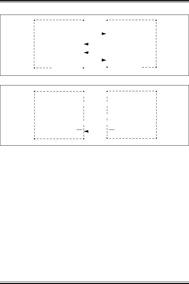
FIGURE 16-2: SPI MASTER/SLAVE CONNECTION
PROCESSOR 1 (SPI Master) |
|
|
|
PROCESSOR 2 (SPI Slave) |
|
|
|||
|
|
|
SDOx |
|
SDIx |
|
Serial Receive Buffer |
|
Serial Receive Buffer |
||
(SPIxRXB) |
|
|
|
(SPIxRXB) |
Shift Register |
SDIx |
|
SDOx |
Shift Register |
(SPIxSR) |
|
|
|
(SPIxSR) |
MSb |
LSb |
|
MSb |
LSb |
Serial Transmit Buffer |
|
Serial Transmit Buffer |
||
(SPIxTXB) |
|
|
|
(SPIxTXB) |
SPI Buffer |
SCKx |
Serial Clock |
SCKx |
SPI Buffer |
|
||||
(SPIxBUF)(2) |
|
|
|
(SPIxBUF)(2) |
|
|
|
|
|
|
|
|
|
|
|
|
|
|
|
|
|
|
|
|
|
|
|
|
|
|
|
|
|
|
|
|
|
|
|
|
(1) |
|
||||||||||||||||||||||||||||||||||||||
|
|
|
|
|
|
|
|
|
|
|
|
|
|
|
|
|
|
|
|
|
|
|
|
|
|
|
|
|
|
|
|
|
|
|
SSx |
|
|||||||||||||||||||||||||||||||||||||||
|
|
|
|
|
|
|
|
|
|
|
|
|
|
|
|
|
|
|
|
|
|
|
|
|
|
|
|
|
|
|
|
|
|
|
|
|
|
|
|
|
|
|
|
|
|
|
|
|
|
|
|
|
|
|
|
|
|
|
|
|
|
|
|
|
|
|
|
|
|
|
|
|
|
|
|
|
|
|
|
|
|
|
|
|
|
|
|
|
|
|
|
|
|
|
|
|
|
|
|
|
|
|
|
|
|
|
|
|
|
|
|
|
|
|
|
|
|
|
|
|
|
|
|
|
|
|
|
|
|
|
|
|
|
|
|
|
|
|
|
|
|
|
|
|
|
|
|
|
|
|
|
(MSTEN (SPIxCON1<5>) = 1) |
(SSEN (SPIxCON1<7>) = 1 and MSTEN (SPIxCON1<5>) = 0) |
||||||||||||||||||||||||||||||||||||||||||||||||||||||||||||||||||||||||||
Note 1: Using the SSx pin in Slave mode of operation is optional.
2:User application must write transmit data to or read received data from SPIxBUF. The SPIxTXB and SPIxRXB registers are memory mapped to SPIxBUF.
FIGURE 16-3: SPI MASTER, FRAME MASTER CONNECTION DIAGRAM
|
|
|
|
|
|
|
|
|
|
|
|
|
|
|
|
|
|
|
|
|
|
|
|
|
|
|
|
|
|
|
|
|
|
|
|
|
|
|
|
|
|
|
|
|
|
|
|
|
|
|
|
|
|
|
|
|
|
|
|
|
|
|
|
|
|
|
|
|
|
|
|
|
|
|
|
|
|
|
dsPIC33F |
|
|
|
|
|
|
|
|
|
|
|
|
|
PROCESSOR 2 |
|
|
||||||||||||||||||||||||||||||||||||||||
|
|
|
|
|
|
|
|
|
|
|
|
|
|
||||||||||||||||||||||||||||||||||||||||||||||||||||||
|
|
|
|
|
|
|
|
|
|
|
|
|
|
|
|
|
|
|
|
|
|
|
|
SDOx |
|
|
|
|
|
|
SDIx |
|
|
||||||||||||||||||||||||||||||||||
|
|
|
|
|
|
|
|
|
|
|
|
|
|
|
|
|
|
|
|
|
|
|
|
|
|
|
|
|
|
|
|
||||||||||||||||||||||||||||||||||||
|
|
|
|
|
|
|
|
|
|
|
|
|
|
|
|
|
|
|
|
|
|
|
|
|
|
|
|
|
|
|
|
||||||||||||||||||||||||||||||||||||
|
|
|
|
|
|
|
|
|
|
|
|
|
|
|
|
|
|
|
|
|
|
|
|
|
|
|
|
|
|
|
|
||||||||||||||||||||||||||||||||||||
|
|
|
|
|
|
|
|
|
|
|
|
|
|
|
|
|
|
|
|
|
|
|
|
|
|
|
|
|
|
|
|||||||||||||||||||||||||||||||||||||
|
|
|
|
|
|
|
|
|
|
|
|
|
|
|
|
|
|
|
|
|
|
|
|
|
|
|
|
|
|
|
|||||||||||||||||||||||||||||||||||||
|
|
|
|
|
|
|
|
|
|
|
|
|
|
|
|
|
|
|
|
|
|
|
|
|
SDIx |
|
|
|
|
|
|
SDOx |
|
|
|||||||||||||||||||||||||||||||||
|
|
|
|
|
|
|
|
|
|
|
|
|
|
|
|
|
|
|
|
|
|
|
|
|
|
|
|
|
|
|
|
|
|||||||||||||||||||||||||||||||||||
|
|
|
|
|
|
|
|
|
|
|
|
|
|
|
|
|
|
|
|
|
|
|
|
|
|
|
|
|
|
|
|
|
|||||||||||||||||||||||||||||||||||
|
|
|
|
|
|
|
|
|
|
|
|
|
|
|
|
|
|
|
|
|
|
|
|
|
|
|
|
|
|
|
|
|
|||||||||||||||||||||||||||||||||||
|
|
|
|
|
|
|
|
|
|
|
|
|
|
|
|
|
|
|
|
|
|
|
|
|
|
|
|
|
|
|
|
|
|||||||||||||||||||||||||||||||||||
|
|
|
|
|
|
|
|
|
|
|
|
|
|
|
|
|
|
|
|
|
|
|
|
|
|
|
|
|
|
|
|
||||||||||||||||||||||||||||||||||||
|
Serial Clock |
||||||||||||||||||||||||||||||||||||||||||||||||||||||||||||||||||
|
|
|
|
|
|
|
|
|
|
|
|
|
|
|
|
|
|
|
|
|
|
|
|
|
|
|
|
|
|||||||||||||||||||||||||||||||||||||||
|
|
|
|
|
|
|
|
|
|
|
|
|
|
|
|
|
|
|
|
|
|
|
|
|
SCKx |
|
|
|
|
|
|
|
|
|
|
|
|
|
|
|
|
|
|
|
|
|
|
|
|
|
|
|
|
|
|
|
|
|
|||||||||
|
|
|
|
|
|
|
|
|
|
|
|
|
|
|
|
|
|
|
|
|
|
|
|
|
|
|
|
|
|
|
|
|
|
|
|
|
|
|
|||||||||||||||||||||||||||||
|
|
|
|
|
|
|
|
|
|
|
|
|
|
|
|
|
|
|
|
|
|
|
|
|
|
|
|
|
|
|
SCKx |
|
|
||||||||||||||||||||||||||||||||||
|
|
|
|
|
|
|
|
|
|
|
|
|
|
|
|
|
|
|
|
|
|
|
|
|
|
|
|
|
|
|
|
|
|
|
|
|
|
|
|
|
|
|
|
|
|
|
|
|
|
|
|
|
|
|
|
|
|
|
|
|
|
|
|
|
|
|
|
|
|
|
|
|
|
|
|
|
|
|
|
|
|
|
|
|
|
|
|
|
|
|
|
|
|
|
SSx |
|
|
Frame Sync |
|
|
SSx |
|
|
|
|
|
|
|
|
|
|
|
|
|
|
|
|
|
|
|
|
|
|
|
|
|
|
|
|||||||
|
|
|
|
|
|
|
|
|
|
|
|
|
|
|
|
|
|
|
|
|
|
|
|
|
|
|
|
|
|
|
|
|
|
|
|
|
|
|
|
|
|
|
|
|
|
|
|
|
|
|
|
|
|
|
|
|
|
||||||||||
|
|
|
|
|
|
|
|
|
|
|
|
|
|
|
|
|
|
|
|
|
|
|
|
|
|
|
|
|
|
|
|
|
|
|
|
|
|
|
|
|
|
|
|
|
|
||||||||||||||||||||||
|
|
|
|
|
|
|
|
|
|
|
|
|
|
|
|
|
|
|
|
|
|
|
|
|
|
|
|
|
|
|
|
|
Pulse |
|
|
|
|
|
|
|
|
|
|
|
|
|
|||||||||||||||||||||
|
|
|
|
|
|
|
|
|
|
|
|
|
|
|
|
|
|
|
|
|
|
|
|
|
|
|
|
|
|
|
|
|
|
|
|||||||||||||||||||||||||||||||||
|
|
|
|
|
|
|
|
|
|
|
|
|
|
|
|
|
|
|
|
|
|
|
|
|
|
|
|
|
|
|
|
|
|
|
|
|
|
|
|
|
|
|
|
|
|
|
|
|
|
|
|
|
|
|
|
|
|
|
|
|
|
|
|
|
|
|
|
|
|
|
|
|
|
|
|
|
|
|
|
|
|
|
|
|
|
|
|
|
|
|
|
|
|
|
|
|
|
|
|
|
|
|
|
|
|
|
|
|
|
|
|
|
|
|
|
|
|
|
|
|
|
|
|
|
|
|
|
|
|
|
|
|
|
|
|
FIGURE 16-4: SPI MASTER, FRAME SLAVE CONNECTION DIAGRAM
dsPIC33F |
|
PROCESSOR 2 |
|
||
|
SDOx 
 SDIx
SDIx
SDIx 
 SDOx
SDOx
Serial Clock
SCKx  SCKx
SCKx
SSx 

 SSx
SSx
Frame Sync
Pulse
♥ 2007 Microchip Technology Inc.
Preliminary
DS70283B-page 179
dsPIC33FJ32MC202/204 and dsPIC33FJ16MC304
FIGURE 16-5: SPI SLAVE, FRAME MASTER CONNECTION DIAGRAM
dsPIC33F |
|
|
|
|
|
|
|
|
|
|
|
|
|
PROCESSOR 2 |
||||||||||||||||||||||||||||||||
|
|
|
|
|||||||||||||||||||||||||||||||||||||||||||
|
|
|
|
|
|
|
|
|
|
|
|
|
||||||||||||||||||||||||||||||||||
|
|
|
|
|
|
|
|
|
|
|
|
|
SDOx |
|
|
|
|
|
|
SDIx |
||||||||||||||||||||||||||
|
|
|
|
|
|
|
|
|
|
|
|
|
|
|
|
|
|
|
||||||||||||||||||||||||||||
|
|
|
|
|
|
|
|
|
|
|
|
|
|
|
|
|
|
|
||||||||||||||||||||||||||||
|
|
|
|
|
|
|
|
|
|
|
|
|
|
|
|
|
|
|
||||||||||||||||||||||||||||
|
|
|
|
|
|
|
|
|
|
|
|
|
|
|
|
|
|
|
||||||||||||||||||||||||||||
|
|
|
|
|
|
|
|
|
|
|
|
|
|
|
|
|
|
|
||||||||||||||||||||||||||||
|
|
|
|
|
|
|
|
|
|
|
|
|
|
SDIx |
|
|
|
|
|
SDOx |
||||||||||||||||||||||||||
|
|
|
|
|
|
|
|
|
|
|
|
|
|
|
|
|
|
|
||||||||||||||||||||||||||||
|
|
|
|
|
|
|
|
|
|
|
|
|
|
|
|
|
|
|
||||||||||||||||||||||||||||
|
|
|
|
|
|
|
|
|
|
|
|
|
|
|
|
|
|
|
||||||||||||||||||||||||||||
|
|
|
|
|
|
|
|
|
|
|
|
|
|
|
|
|
|
|
||||||||||||||||||||||||||||
|
|
|
|
|
|
|
|
|
|
|
|
|
|
|
|
|
|
|
||||||||||||||||||||||||||||
|
|
|
|
|
|
|
|
|
|
|
|
|
|
|
|
|
|
|
|
|
|
|||||||||||||||||||||||||
|
|
|
|
|
|
|
|
|
|
|
|
|
SCKx |
Serial Clock |
|
|
||||||||||||||||||||||||||||||
|
|
|
|
|
|
|
|
|
|
|
|
|
|
|||||||||||||||||||||||||||||||||
|
|
|
|
|
|
|
|
|
|
|
|
|
|
|
|
|
|
SCKx |
||||||||||||||||||||||||||||
|
|
|
|
|||||||||||||||||||||||||||||||||||||||||||
|
|
|
|
|
|
|
|
|
|
|
|
|
|
|
|
|
|
|
|
|
|
|
|
|
|
|
|
|
|
|
|
|
|
|
|
|
|
|
|
|
|
|
|
|
|
|
|
|
|
|
|
|
|
|
|
|
|
|
|
|
|
SSx |
|
|
|
|
|
|
SSx |
|
|
|
|
|
|
|
|
|
|
|
|
|
|
|
|
|
|
||||||
|
|
|
|
|
|
|
|
|
|
|
|
|
|
|
|
|
|
|
|
|
Frame Sync |
|
|
|||||||||||||||||||||||
|
|
|
|
|
|
|
|
|
|
|
|
|
|
|
|
|
|
|
|
|
Pulse |
|
|
|||||||||||||||||||||||
|
|
|
|
|
|
|
|
|
|
|
|
|
|
|
|
|
|
|
|
|
|
|||||||||||||||||||||||||
|
|
|
|
|
|
|
|
|
|
|
|
|
|
|
|
|
|
|
|
|
|
|
|
|
|
|
|
|
|
|
|
|
|
|
|
|
|
|
|
|
|
|
|
|
|
|
FIGURE 16-6: SPI SLAVE, FRAME SLAVE CONNECTION DIAGRAM
dsPIC33F |
|
|
PROCESSOR 2 |
|
|||
|
|
SDOx 
 SDIx
SDIx
SDIx 
 SDOx
SDOx
Serial Clock
SCKx 
 SCKx
SCKx
SSx  SSx
SSx
Frame Sync
Pulse
EQUATION 16-1: RELATIONSHIP BETWEEN DEVICE AND SPI CLOCK SPEED
FSCK = |
FCY |
|
|
|
|
Primary Prescaler * Secondary Prescaler |
|
|
|
|
|
TABLE 16-1: SAMPLE SCKx FREQUENCIES |
|
|
FCY = 40 MHz |
|
|
Secondary Prescaler Settings |
|
||
|
|
|
|
|
|
|
|
1:1 |
2:1 |
4:1 |
6:1 |
8:1 |
|
|
|
|||||
|
|
|
|
|
|
|
Primary Prescaler Settings |
1:1 |
Invalid |
Invalid |
10000 |
6666.67 |
5000 |
|
4:1 |
10000 |
5000 |
2500 |
1666.67 |
1250 |
|
16:1 |
2500 |
1250 |
625 |
416.67 |
312.50 |
|
64:1 |
625 |
312.5 |
156.25 |
104.17 |
78.125 |
FCY = 5 MHz |
|
|
|
|
|
|
|
|
|
|
|
|
|
Primary Prescaler Settings |
1:1 |
5000 |
2500 |
1250 |
833 |
625 |
|
4:1 |
1250 |
625 |
313 |
208 |
156 |
|
16:1 |
313 |
156 |
78 |
52 |
39 |
|
64:1 |
78 |
39 |
20 |
13 |
10 |
Note: SCKx frequencies shown in kHz.
DS70283B-page 180 |
Preliminary |
♥ 2007 Microchip Technology Inc. |

dsPIC33FJ32MC202/204 and dsPIC33FJ16MC304
REGISTER 16-1: SPIxSTAT: SPIx STATUS AND CONTROL REGISTER
R/W-0 |
|
U-0 |
R/W-0 |
U-0 |
U-0 |
U-0 |
U-0 |
U-0 |
||||||
SPIEN |
|
— |
SPISIDL |
|
— |
|
— |
|
|
— |
— |
|
— |
|
bit 15 |
|
|
|
|
|
|
|
|
|
|
|
|
|
bit 8 |
|
|
|
|
|
|
|
|
|
|
|
|
|
||
U-0 |
|
R/C-0 |
U-0 |
U-0 |
U-0 |
U-0 |
R-0 |
R-0 |
||||||
— |
|
SPIROV |
— |
|
— |
|
— |
|
|
— |
SPITBF |
|
SPIRBF |
|
bit 7 |
|
|
|
|
|
|
|
|
|
|
|
|
|
bit 0 |
|
|
|
|
|
|
|
|
|
|
|
|
|
|
|
Legend: |
|
|
C = Clearable bit |
|
|
|
|
|
|
|
|
|
|
|
R = Readable bit |
|
W = Writable bit |
|
|
U = Unimplemented bit, read as ‘0’ |
|
||||||||
-n = Value at POR |
‘1’ = Bit is set |
|
|
‘0’ = Bit is cleared |
|
|
x = Bit is unknown |
|||||||
bit 15 |
SPIEN: SPIx Enable bit |
|
|
|
|
|
|
|
|
|
|
|||
|
1 |
= Enables module and configures SCKx, SDOx, SDIx and |
|
as serial port pins |
|
|||||||||
|
SSx |
|
||||||||||||
|
0 |
= Disables module |
|
|
|
|
|
|
|
|
|
|
||
bit 14 |
Unimplemented: Read as ‘0’ |
|
|
|
|
|
|
|
|
|
|
|||
bit 13 |
SPISIDL: Stop in Idle Mode bit |
|
|
|
|
|
|
|
|
|
|
|||
|
1 |
= Discontinue module operation when device enters Idle mode |
|
|
|
|||||||||
|
0 |
= Continue module operation in Idle mode |
|
|
|
|
|
|||||||
bit 12-7 |
Unimplemented: Read as ‘0’ |
|
|
|
|
|
|
|
|
|
|
|||
bit 6 |
SPIROV: Receive Overflow Flag bit |
|
|
|
|
|
|
|
|
|||||
|
1 |
= A new byte/word is completely received and discarded. The user software has not read the |
||||||||||||
|
0 |
previous data in the SPIxBUF register. |
|
|
|
|
|
|
|
|
||||
|
= No overflow has occurred. |
|
|
|
|
|
|
|
|
|
|
|||
bit 5-2 |
Unimplemented: Read as ‘0’ |
|
|
|
|
|
|
|
|
|
|
|||
bit 1 |
SPITBF: SPIx Transmit Buffer Full Status bit |
|
|
|
|
|
||||||||
|
1 |
= Transmit not yet started, SPIxTXB is full |
|
|
|
|
|
|||||||
|
0 |
= Transmit started, SPIxTXB is empty |
|
|
|
|
|
|
|
|
||||
|
Automatically set in hardware when CPU writes SPIxBUF location, loading SPIxTXB |
|
||||||||||||
|
Automatically cleared in hardware when SPIx module transfers data from SPIxTXB to SPIxSR |
|||||||||||||
bit 0 |
SPIRBF: SPIx Receive Buffer Full Status bit |
|
|
|
|
|
||||||||
|
1 |
= Receive complete, SPIxRXB is full |
|
|
|
|
|
|
|
|
||||
|
0 |
= Receive is not complete, SPIxRXB is empty |
|
|
|
|
|
|||||||
|
Automatically set in hardware when SPIx transfers data from SPIxSR to SPIxRXB |
|
||||||||||||
|
Automatically cleared in hardware when core reads SPIxBUF location, reading SPIxRXB |
|
||||||||||||
♥ 2007 Microchip Technology Inc.
Preliminary
DS70283B-page 181

dsPIC33FJ32MC202/204 and dsPIC33FJ16MC304
REGISTER 16-2: SPIXCON1: SPIx CONTROL REGISTER 1
U-0 |
|
U-0 |
U-0 |
R/W-0 |
R/W-0 |
R/W-0 |
R/W-0 |
R/W-0 |
||
— |
|
— |
— |
|
DISSCK |
DISSDO |
|
MODE16 |
SMP |
CKE(1) |
bit 15 |
|
|
|
|
|
|
|
|
|
bit 8 |
|
|
|
|
|
|
|
|
|
|
|
R/W-0 |
|
R/W-0 |
R/W-0 |
R/W-0 |
R/W-0 |
R/W-0 |
R/W-0 |
R/W-0 |
||
SSEN |
|
CKP |
MSTEN |
|
|
SPRE<2:0> |
|
PPRE<1:0> |
||
bit 7 |
|
|
|
|
|
|
|
|
|
bit 0 |
|
|
|
|
|
|
|
|
|
|
|
Legend: |
|
|
|
|
|
|
|
|
|
|
R = Readable bit |
|
W = Writable bit |
|
U = Unimplemented bit, read as ‘0’ |
|
|||||
-n = Value at POR |
‘1’ = Bit is set |
|
‘0’ = Bit is cleared |
x = Bit is unknown |
||||||
bit 15-13 |
Unimplemented: Read as ‘0’ |
|
|
|
|
|
|
|||
bit 12 |
DISSCK: Disable SCKx pin bit (SPI Master modes only) |
|
|
|
||||||
|
1 |
= Internal SPI clock is disabled, pin functions as I/O |
|
|
|
|||||
|
0 |
= Internal SPI clock is enabled |
|
|
|
|
|
|||
bit 11 |
DISSDO: Disable SDOx pin bit |
|
|
|
|
|
|
|||
|
1 |
= SDOx pin is not used by module; pin functions as I/O |
|
|
|
|||||
|
0 |
= SDOx pin is controlled by the module |
|
|
|
|
|
|||
bit 10 |
MODE16: Word/Byte Communication Select bit |
|
|
|
||||||
|
1 |
= Communication is word-wide (16 bits) |
|
|
|
|
|
|||
|
0 |
= Communication is byte-wide (8 bits) |
|
|
|
|
|
|||
bit 9 |
SMP: SPIx Data Input Sample Phase bit |
|
|
|
|
|
||||
|
Master mode: |
|
|
|
|
|
|
|
|
|
|
1 |
= Input data sampled at end of data output time |
|
|
|
|||||
|
0 |
= Input data sampled at middle of data output time |
|
|
|
|||||
|
Slave mode: |
|
|
|
|
|
|
|
|
|
|
SMP must be cleared when SPIx is used in Slave mode. |
|
|
|
||||||
bit 8 |
CKE: SPIx Clock Edge Select bit(1) |
|
|
|
|
|
||||
|
1 |
= Serial output data changes on transition from active clock state to Idle clock state (see bit 6) |
||||||||
|
0 |
= Serial output data changes on transition from Idle clock state to active clock state (see bit 6) |
||||||||
bit 7 |
SSEN: Slave Select Enable bit (Slave mode) |
|
|
|
||||||
|
1 |
= SSx pin used for Slave mode |
|
|
|
|
|
|||
|
0 |
= SSx pin not used by module. Pin controlled by port function. |
|
|
||||||
bit 6 |
CKP: Clock Polarity Select bit |
|
|
|
|
|
|
|||
|
1 |
= Idle state for clock is a high level; active state is a low level |
|
|
||||||
|
0 |
= Idle state for clock is a low level; active state is a high level |
|
|
||||||
bit 5 |
MSTEN: Master Mode Enable bit |
|
|
|
|
|
||||
|
1 |
= Master mode |
|
|
|
|
|
|
||
|
0 |
= Slave mode |
|
|
|
|
|
|
||
Note 1: The CKE bit is not used in the Framed SPI modes. Program this bit to ‘0’ for the Framed SPI modes (FRMEN = 1).
DS70283B-page 182 |
Preliminary |
♥ 2007 Microchip Technology Inc. |

dsPIC33FJ32MC202/204 and dsPIC33FJ16MC304
REGISTER 16-2: SPIXCON1: SPIx CONTROL REGISTER 1 (CONTINUED)
bit 4-2 |
SPRE<2:0>: Secondary Prescale bits (Master mode) |
|
|
111 = Secondary prescale 1:1 |
|
|
110 = Secondary prescale 2:1 |
|
|
. |
|
|
. |
|
|
. |
|
|
000 = Secondary prescale 8:1 |
|
bit 1-0 |
PPRE<1:0>: Primary Prescale bits (Master mode) |
|
|
11 |
= Primary prescale 1:1 |
|
10 |
= Primary prescale 4:1 |
|
01 |
= Primary prescale 16:1 |
|
00 |
= Primary prescale 64:1 |
Note 1: |
The CKE bit is not used in the Framed SPI modes. Program this bit to ‘0’ for the Framed SPI modes |
|
|
(FRMEN = 1). |
|
♥ 2007 Microchip Technology Inc.
Preliminary
DS70283B-page 183

dsPIC33FJ32MC202/204 and dsPIC33FJ16MC304
REGISTER 16-3: SPIxCON2: SPIx CONTROL REGISTER 2
R/W-0 |
|
R/W-0 |
R/W-0 |
U-0 |
U-0 |
U-0 |
U-0 |
U-0 |
|||||
FRMEN |
|
SPIFSD |
FRMPOL |
|
— |
— |
|
— |
— |
|
— |
||
bit 15 |
|
|
|
|
|
|
|
|
|
|
|
|
bit 8 |
|
|
|
|
|
|
|
|
|
|
|
|
||
U-0 |
|
U-0 |
U-0 |
U-0 |
U-0 |
U-0 |
R/W-0 |
U-0 |
|||||
— |
|
— |
— |
|
— |
— |
|
— |
FRMDLY |
|
— |
||
bit 7 |
|
|
|
|
|
|
|
|
|
|
|
|
bit 0 |
|
|
|
|
|
|
|
|
|
|
|
|
|
|
Legend: |
|
|
|
|
|
|
|
|
|
|
|
|
|
R = Readable bit |
|
W = Writable bit |
|
|
|
U = Unimplemented bit, read as ‘0’ |
|
||||||
-n = Value at POR |
‘1’ = Bit is set |
|
|
|
‘0’ = Bit is cleared |
|
x = Bit is unknown |
|
|||||
bit 15 |
FRMEN: Framed SPIx Support bit |
|
|
|
|
|
|
||||||
|
1 |
= Framed SPIx support enabled |
|
pin used as frame sync pulse input/output) |
|
||||||||
|
(SSx |
|
|||||||||||
|
0 |
= Framed SPIx support disabled |
|
|
|
|
|
|
|||||
bit 14 |
SPIFSD: Frame Sync Pulse Direction Control bit |
|
|
|
|
||||||||
|
1 |
= Frame sync pulse input (slave) |
|
|
|
|
|
|
|||||
|
0 |
= Frame sync pulse output (master) |
|
|
|
|
|
|
|||||
bit 13 |
FRMPOL: Frame Sync Pulse Polarity bit |
|
|
|
|
|
|
||||||
|
1 |
= Frame sync pulse is active-high |
|
|
|
|
|
|
|||||
|
0 |
= Frame sync pulse is active-low |
|
|
|
|
|
|
|||||
bit 12-2 |
Unimplemented: Read as ‘0’ |
|
|
|
|
|
|
|
|
|
|||
bit 1 |
FRMDLY: Frame Sync Pulse Edge Select bit |
|
|
|
|
||||||||
|
1 |
= Frame sync pulse coincides with first bit clock |
|
|
|
|
|||||||
|
0 |
= Frame sync pulse precedes first bit clock |
|
|
|
|
|||||||
bit 0 |
Unimplemented: This bit must not be set to ‘1’ by the user application. |
|
|
|
|||||||||
DS70283B-page 184 |
Preliminary |
♥ 2007 Microchip Technology Inc. |

dsPIC33FJ32MC202/204 and dsPIC33FJ16MC304
17.0INTER-INTEGRATED CIRCUIT (I2C)
Note: This data sheet summarizes the features of the dsPIC33FJ32MC202/204 and dsPIC33FJ16MC304 devices. It is not intended to be a comprehensive reference source. To complement the information in this data sheet, refer to the “dsPIC33F Family Reference Manual”. Please see the Microchip web site (www.microchip.com) for the latest dsPIC33F Family Reference Manual sections.
The Inter-Integrated Circuit (I2C) module provides complete hardware support for both Slave and MultiMaster modes of the I2C serial communication standard, with a 16-bit interface.
The I2C module has a 2-pin interface:
•The SCLx pin is clock.
•The SDAx pin is data.
The I2C module offers the following key features:
•I2C interface supporting both Master and Slave modes of operation.
•I2C Slave mode supports 7 and 10-bit address.
•I2C Master mode supports 7 and 10-bit address.
•I2C port allows bidirectional transfers between master and slaves.
•Serial clock synchronization for I2C port can be used as a handshake mechanism to suspend and resume serial transfer (SCLREL control).
•I2C supports multi-master operation, detects bus collision and arbitrates accordingly.
17.1Operating Modes
The hardware fully implements all the master and slave functions of the I2C Standard and Fast mode specifications, as well as 7 and 10-bit addressing.
The I2C module can operate either as a slave or a master on an I2C bus.
The following types of I2C operation are supported:
•I2C slave operation with 7-bit address
•I2C slave operation with 10-bit address
•I2C master operation with 7 or 10-bit address
For details about the communication sequence in each of these modes, refer to the “dsPIC33F Family Reference Manual”. Please see the Microchip web site (www.microchip.com) for the latest dsPIC33F Family Reference Manual sections.
17.2I2C Registers
I2CxCON and I2CxSTAT are control and status registers, respectively. The I2CxCON register is readable and writable. The lower six bits of I2CxSTAT are read-only. The remaining bits of the I2CSTAT are read/write:
•I2CxRSR is the shift register used for shifting data.
•I2CxRCV is the receive buffer and the register to which data bytes are written, or from which data bytes are read.
•I2CxTRN is the transmit register to which bytes are written during a transmit operation.
•The I2CxADD register holds the slave address.
•A status bit, ADD10, indicates 10-bit Address mode.
•The I2CxBRG acts as the Baud Rate Generator (BRG) reload value.
In receive operations, I2CxRSR and I2CxRCV together form a double-buffered receiver. When I2CxRSR receives a complete byte, it is transferred to I2CxRCV, and an interrupt pulse is generated.
17.3I2C Interrupts
The I2C module generates two interrupt flags:
•MI2CxIF (I2C Master Events Interrupt flag)
•SI2CxIF (I2C Slave Events Interrupt flag).
A separate interrupt is generated for all I2C error conditions.
17.4Baud Rate Generator
In I2C Master mode, the reload value for the Baud Rate Generator (BRG) is located in the I2CxBRG register. When the BRG is loaded with this value, the BRG counts down to zero and stops until another reload has taken place. If clock arbitration is taking place, for example, the BRG is reloaded when the SCLx pin is sampled high.
As per the I2C standard, FSCL can be 100 kHz or 400 kHz. However, the user application can specify any baud rate up to 1 MHz. I2CxBRG values of ‘0’ or ‘1’ are illegal.
EQUATION 17-1: SERIAL CLOCK RATE
I2CxBRG = ( |
FCY |
|
FCY |
|
|
– |
|
) – 1 |
|
FSCL |
10,000,000 |
|||
|
|
|
|
|
♥ 2007 Microchip Technology Inc.
Preliminary
DS70283B-page 185

dsPIC33FJ32MC202/204 and dsPIC33FJ16MC304
FIGURE 17-1: I2C™ BLOCK DIAGRAM (X = 1)
|
|
|
|
|
|
|
|
|
|
|
|
|
|
I2CxRCV |
|
|||||||||||
|
|
|
|
|
|
|
|
|
|
|
|
|
|
|
|
|
|
|
|
|
|
|
|
|
|
|
|
|
|
|
|
|
|
|
|
|
|
|
|
|
|
|
|
|
|
|
|
|
|
|
|
|
|
|
|
|
|
|
|
|
|
|
|
|
|
|
|
|
|
|
|
|
|
|
|
|
|
|
|
|
|
|
|
|
|
|
|
|
|
|
Shift |
|
|
|
|
|
|
|
|
|
|
|
|
||||
SCLx |
|
|
|
|
|
|
|
Clock |
|
|
|
|
|
|
|
|
|
|
|
|
||||||
|
|
|
|
|
|
|||||||||||||||||||||
|
|
|
|
|
|
|
|
|
|
|
|
|
|
I2CxRSR |
|
|
|
|
|
|||||||
|
|
|
|
|
|
|
|
|
|
|||||||||||||||||
|
|
|
|
|
|
|
|
|
|
|
|
|
|
|
|
|
|
|
|
|
|
|
|
|
|
|
|
|
|
|
|
|
|
|
|
|
|
|
|
|
|
|
|
|
|
|
|
LSb |
|
|
|
|
|
|
|
|
|
|
|
|
|
|
|
|
|
|
|
|
|
|
|
|
|
|
|
|
|
|
|
|
|
|
|
|
|
|
|
|
|
|
|
|
|
|
|
|
|
|
|
|
|
|
|
|
|
|
|
|
|
|
|
|
|
|
|
|
|
|
|
|
|
|
|
|
|
|
|
|
|
|
|
|
|
|
SDAx |
|
|
|
|
|
|
|
|
|
|
|
|
|
|
|
|
|
|
|
|
Address Match |
|||||
|
|
|
|
|
|
|
|
|
|
|
Match Detect |
|
||||||||||||||
|
|
|
|
|
|
|
|
|
|
|
|
|
|
|
|
|
||||||||||
|
|
|
|
|
|
|
|
|
|
|
|
|
|
|
|
|
|
|
||||||||
|
|
|
|
|
|
|
|
|
|
|
|
|
|
|
|
|
|
|
|
|
|
|
|
|
|
|
|
|
|
|
|
|
|
|
|
|
|
|
|
|
|
|
|
|
|
|
|
|
|
|
|
|
|
|
|
|
|
|
|
|
|
|
|
|
|
|
|
|
|
|
|
|
|
|
|
|
|
|
|
|
I2CxADD
|
|
|
|
|
|
|
|
Start and Stop |
|
|
|
|
|
|
|
|
|
|
|
|
|
|
|
|
|
|
|
|
|
|
|
|
|
|
|
|
|
|
|
Bit Detect |
|
|
|
|
|
|
|
|
|
|
|
|
|
|
|
|
|
|
|
|
|
|
|
|
|
|
|
|
|
|
|
|
|
|
|
|
|
|
|
|
|
|
|
|
|
|
|
Start and Stop |
|
|
|
|
|
|
|
|
|
|
|
|
|
|
|
|
|
|
|
|
|
|
|
|
|
|
|
|
|
|
|
Bit Generation |
|
|
|
|
Logic |
|
|
|
|
|
|
|
|
|
|
|
|
|
|
|
|
|
|
|
|
|
|
|
|
|
|
|
|
|
|
|
|
|
|
|
|
|
|
|
|
|
|
Collision |
|
|
|
|
|
|
|
|
|
|
|
|
|
|
|
|
|
|
|
|
|
||
|
|
|
|
|
|
|
|
|
|
|
|
|
|
||
|
|
|
|
|
|
|
|
|
|
|
|
Control |
|
|
|
|
|
|
|
|
|
|
|
|
|
|
|
|
|
||
|
|
|
|
|
|
|
|
Detect |
|
|
|
|
|
|
|
|
|
|
|
|
|
|
|
|
|
|
|
|
|
|
|
|
|
|
|
|
|
|
|
|
|
|
|
|
|
|
|
|
|
|
|
|
|
|
|
|
|
|
|
|
|
|
|
|
|
|
|
|
|
|
|
|
|
|
|
|
|
|
|
|
|
|
|
|
|
|
|
Acknowledge |
|
|
|
|
|
|
|
|
|
|
|
|
|
|
|
Generation |
|
|
|
|
|
|
|
|
|
|
|
|
|
|
|
|
|
|
|
|
|
|
|
|
|
|
|
|
|
|
|
|
|
|
|
|
|
|
|
|
|
|
|
|
|
|
|
Clock |
|
|
|
|
|
|
|
|
|
|
|
|
|
|
|
Stretching |
|
|
|
|
|
|
|
|
|
|
|
|
|
|
|
|
|
|
|
|
|
|
|
|
|
|
|
|
|
|
|
|
|
|
|
|
|
|
|
|
|
|
|
|
|
|
|
I2CxTRN |
|
|
|
|
|
|
|
|
|
|
|
|
|
|
|
|
|
|
|
|
|
|
|
|
|
|
|
|
|
|
|
|
|
|
|
|
|
|
|
|
|
|
|
|
|
|
|
|
LSb |
|
|
||||
 Shift Clock
Reload
Control

 BRG Down Counter

TCY/2
Internal
Data Bus
Read
|
Write |
I2CxMSK |
|
Write |
Read |
Read |
|
|
Write |
I2CxSTAT |
|
|
Read |
|
Write |
I2CxCON |
|
|
Read |
Write |
|
Read |
|
|
Write |
I2CxBRG |
|
|
Read |
|
|
|
|
|
|
|
|
|
|
DS70283B-page 186 |
Preliminary |
♥ 2007 Microchip Technology Inc. |
||

dsPIC33FJ32MC202/204 and dsPIC33FJ16MC304
17.5I2C Module Addresses
The 10-bit I2CxADD register contains the Slave mode addresses.
If the A10M bit (I2CxCON<10>) is ‘0’, the address is interpreted by the module as a 7-bit address. When an address is received, it is compared to the 7 Least Significant bits of the I2CxADD register.
If the A10M bit is ‘1’, the address is assumed to be a 10-bit address. When an address is received, it is compared with the binary value, ‘11110 A9 A8’ (where A9 and A8 are two Most Significant bits of I2CxADD). If that value matches, the next address will be compared with the Least Significant 8 bits of I2CxADD, as specified in the 10-bit addressing protocol.
TABLE 17-1: 7-BIT I2C™ SLAVE
|
ADDRESSES SUPPORTED BY |
|
dsPIC33FJ32MC202/204 and |
|
dsPIC33FJ16MC304 |
0x00 |
General call address or Start byte |
0x01-0x03 |
Reserved |
0x04-0x07 |
Hs mode Master codes |
0x08-0x77 |
Valid 7-bit addresses |
0x78-0x7b |
Valid 10-bit addresses |
|
(lower 7 bits) |
0x7c-0x7f |
Reserved |
17.6Slave Address Masking
The I2CxMSK register (Register 17-3) designates address bit positions as “don’t care” for both 7-bit and 10-bit Address modes. Setting a particular bit location (= 1) in the I2CxMSK register causes the slave module to respond, whether the corresponding address bit value is a ‘0’ or ‘1’. For example, when I2CxMSK is set to ‘00100000’, the Slave module will detect both addresses, ‘0000000’ and ‘00100000’.
To enable address masking, the IPMI (Intelligent Peripheral Management Interface) must be disabled by clearing the IPMIEN bit (I2CxCON<11>).
17.7IPMI Support
The control bit IPMIEN enables the module to support the Intelligent Peripheral Management Interface (IPMI). When this bit is set, the module accepts and acts upon all addresses.
17.8General Call Address Support
The general call address can address all devices. When this address is used, all devices should, in theory, respond with an Acknowledgement.
The general call address is one of eight addresses reserved for specific purposes by the I2C protocol. It consists of all ‘0’s with R_W = 0.
The general call address is recognized when the General Call Enable (GCEN) bit is set (I2CxCON<7> = 1). When the interrupt is serviced, the source for the interrupt can be checked by reading the contents of the I2CxRCV to determine if the address was device-specific or a general call address.
17.9Automatic Clock Stretch
In Slave modes, the module can synchronize buffer reads and write to the master device by clock stretching.
17.9.1TRANSMIT CLOCK STRETCHING
Both 10-bit and 7-bit Transmit modes implement clock stretching by asserting the SCLREL bit after the falling edge of the ninth clock, if the TBF bit is cleared, indicating the buffer is empty.
In Slave Transmit modes, clock stretching is always performed, irrespective of the STREN bit. The user’s ISR must set the SCLREL bit before transmission is allowed to continue. By holding the SCLx line low, the user application has time to service the ISR and load the contents of the I2CxTRN before the master device can initiate another transmit sequence.
17.9.2RECEIVE CLOCK STRETCHING
The STREN bit in the I2CxCON register can be used to enable clock stretching in Slave Receive mode. When the STREN bit is set, the SCLx pin will be held low at the end of each data receive sequence.
The user’s ISR must set the SCLREL bit before reception is allowed to continue. By holding the SCLx line low, the user application has time to service the ISR and read the contents of the I2CxRCV before the master device can initiate another receive sequence. This prevents buffer overruns.
17.10Software Controlled Clock Stretching (STREN = 1)
When the STREN bit is ‘1’, the software can clear the SCLREL bit to allow software to control the clock stretching.
If the STREN bit is ‘0’, a software write to the SCLREL bit is disregarded and has no effect on the SCLREL bit.
♥ 2007 Microchip Technology Inc.
Preliminary
DS70283B-page 187

dsPIC33FJ32MC202/204 and dsPIC33FJ16MC304
17.11 Slope Control
The I2C standard requires slope control on the SDAx and SCLx signals for Fast mode (400 kHz). The control bit, DISSLW, enables the user application to disable slew rate control if desired. It is necessary to disable the slew rate control for 1 MHz mode.
17.12 Clock Arbitration
Clock arbitration occurs when the master deasserts the SCLx pin (SCLx allowed to float high) during any receive, transmit or Restart/Stop condition. When the SCLx pin is allowed to float high, the Baud Rate Generator (BRG) is suspended from counting until the SCLx pin is actually sampled high. When the SCLx pin is sampled high, the BRG is reloaded with the contents of I2CxBRG and begins counting. This process ensures that the SCLx high time will always be at least one BRG rollover count in the event that the clock is held low by an external device.
17.13Multi-Master Communication, Bus Collision and Bus Arbitration
Multi-Master mode support is achieved by bus arbitration. When the master outputs address/data bits onto the SDAx pin, arbitration takes place when the master outputs a ‘1’ on SDAx by letting SDAx float high while another master asserts a ‘0’. When the SCLx pin floats high, data should be stable. If the expected data on SDAx is a ‘1’ and the data sampled on the SDAx pin = 0, then a bus collision has taken place. The master sets the I2C master events interrupt flag and resets the master portion of the I2C port to its Idle state.
17.14 Peripheral Pin Select Limitations
The I2C module has limited peripheral pin select functionality. When the ALTI2C bit in the FPOR configuration register is set to ‘1’, I2C module uses SDAx/SLCx pins. When ALTI2C bit is ‘0’, I2C module uses ASDAx/ ASCLx pins.
DS70283B-page 188 |
Preliminary |
♥ 2007 Microchip Technology Inc. |