


SYNCHRONOUS SERIAL I/O (SSIO) PORT
8.5.4Enabling the SSIO Interrupts
Each SSIO channel can generate an interrupt request if you enable the individual interrupt as well as globally enabling servicing of all maskable interrupts. The INT_MASK1 register enables and disables individual interrupts. To enable an SSIO interrupt, set the corresponding bit in INT_MASK1 (see Table 8-2 on page 8-2) and execute the EI instruction to globally enable interrupt servicing. See Chapter 5, “Standard and PTS Interrupts,” for more information about interrupts.
8.5.5Determining SSIO Port Status
The SSIO_BAUD register (Figure 8-5 on page 8-10) indicates the current status and value of the down-counter. The SSIOx_CON register (Figure 8-6) indicates whether an underflow or overflow has occurred and whether the channel is ready to transmit or receive. Read the INT_PEND1 register (see Table 8-2 on page 8-2) to determine the status of SSIO interrupts. See Chapter 5, “Standard and PTS Interrupts,” for details about interrupts.
8.6PROGRAMMING CONSIDERATIONS
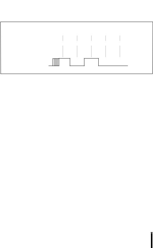
For transmissions, the time that you write to SSIOx_BUF determines the data setup time (the length of time between data being placed on the data pin and the first clock edge on the clock pin). The reason for this anomaly is that the baud-rate down-counter starts when you write to SSIO_BAUD, but the transmission doesn’t start until you write to SSIO x_BUF. The write to SSIOx_BUF can occur at any point during the count. Since the most-significant bit (MSB) doesn’t change until the falling edge of SC x (which is triggered by a counter overflow), the width of the MSB appears to vary (Figure 8-7). If you write to SSIOx_BUF early in the count, the MSB seems relatively long. If you write to SSIOx_BUF late in the count, the MSB seems relatively short.
For example, assume that you write 93H to SSIO_BAUD (the MSB enables the baud-rate generator, and the lower seven bits define the initial count value). As soon as this register is written, the down-counter starts decrementing from 13H. If the counter is at 11H when you write to SSIOx_BUF, the MSB will remain on the data pin for approximately 8.5 µs. If the counter is at 03H when you write to SSIOx_BUF, the MSB will remain on the data pin for only approximately 1.5 µs.
8-13
8XC196Kx, Jx, CA USER’S MANUAL
Clock (SCx pin) |
|
1 |
|
2 |
|
3 |
|
4 |
|
|
"1" "0" "1" "0" "0"
MSB |
B6 |
B5 |
B4 |
B3 |
Data (SDx pin)
A2066-01
Figure 8-7. Variable-width MSB in SSIO Transmissions
NOTE
This condition exists only for the MSB. Once the MSB is clocked out, the remaining bits are clocked out consistently at the programmed frequency.
One way to achieve a consistent MSB bit length is to start the down-count at a fixed time, using these steps:
1.Clear SSIO_BAUD bit 7. This disables the baud-rate generator and clears the remaining bits (BV6:0).
2.Write the byte to be transmitted to SSIOx_BUF.
3.Set the STE bit in SSIOx_CON. This enables transfers and drives the MSB onto the data pin.
4.Disable interrupts.
5.Set the MSB of SSIO_BAUD and write the desired BAUD_VAL to the remaining bits. This enables the baud-rate generator and starts the down count.
6.Rewrite the byte to be transmitted to SSIOx_BUF. This starts the transmission.
7.Enable interrupts.
Using this procedure starts the clock at a known point before each transmission, establishing a predictable MSB bit time. Interrupts are disabled in step 4 and reenabled in step 7; otherwise, an interrupt could cause a similar problem between steps 5 and 6.
8-14

SYNCHRONOUS SERIAL I/O (SSIO) PORT
8.7PROGRAMMING EXAMPLE
This code example configures SSIO0 as a master transmitter to send one byte of data to SSIO1, the slave receiver. First it sets up a window to allow register-direct access to the necessary registers. Next, it configures the clock and data pins. Since SSIO0 is sending data, SC0 (P6.4) and SD0 (P6.5) are configured as special-function complementary outputs. Since SSIO1 is receiving data, SC1 (P6.6) and SD1 (P6.7) are configured as special-function inputs. The example also sets up a register (result) to store the received data byte.
wsr |
equ |
014h:byte |
|
|
p6_dir |
equ |
0d3h:byte |
;window |
to 1fd3h |
p6_mode |
equ |
0d1h:byte |
;window |
to 1fd1h |
p6_reg |
equ |
0d5h:byte |
;window |
to 1fd5h |
ssio_baud equ |
0b4h:byte |
;window |
to 1fb4h |
|
ssio0_con equ |
0b1h:byte |
;window |
to 1fb1h |
|
ssio1_con equ |
0b3h:byte |
;window |
to 1fb3h |
|
ssio0_buf equ |
0b0h:byte |
;window |
to 1fb0h |
|
ssio1_buf equ |
0b2h:byte |
;window |
to 1fb2h |
|
result |
equ |
122h:byte |
;register to store the received data byte |
|
cseg at 2080h |
|
|
|
|
ldb |
wsr,#1fh |
;select |
window 1fh |
|
ldb |
p6_dir,#0c0h |
;set up |
SD1/SC1 as inputs and |
|
|
|
|
;set up |
SD0/SC0 as complementary outputs |
ldb |
p6_mode,#0f0h |
;set up |
SD1/SC1, SD0/SC0 as special-function |
|
ldb |
p6_reg,#0c0h |
;set up |
SD1/SC1 inputs (1), SD0/SC0 outputs (0) |
|
ldb |
ssio_baud,#80h |
;enable |
baud-rate generator at 2 MHz |
|
ldb |
ssio0_con,#0c9h |
;set up |
channel 0 as master transmitter |
|
ldb |
ssio1_con,#08h |
;set up |
channel 1 as slave receiver |
|
ldb |
ssio0_buf,#55h |
;transmit data 55h |
||
d_wait: |
|
|
|
|
jbc |
ssio1_con,0,d_wait |
;wait for data to be received |
||
stb |
ssio1_buf,result |
;store received data in “result” |
||
sjmp $
end
8-15

9
Slave Port

CHAPTER 9
SLAVE PORT
The slave port offers an alternative for communication between two microcontrollers. Traditionally, design engineers have had three options for achieving this communication — a serial link, a parallel bus without a dual-port RAM (DPRAM), or a parallel bus with a DPRAM to hold shared data.
A serial link, the most common method, has several advantages: it uses only two pins from each device, it needs no hardware protocol, and it allows for error detection before data is stored. However, it is relatively slow and involves software overhead to differentiate data, addresses, and commands. A parallel bus increases communication speed, but requires more pins and a rather involved hardware and software protocol. Using a DPRAM offers software flexibility between master and slave devices, but the hardware interconnect uses a demultiplexed bus, which requires even more pins than a simple parallel connection does. The DPRAM is also costly, and error detection can be difficult. The SSIO offers a simple means for implementing a serial link. The multiplexed address/data bus can be used to implement a parallel link, with or without a DPRAM. The slave port offers a fourth alternative.
The slave port offers the advantages of the traditional methods, without their drawbacks. It brings the DPRAM on-chip, inside the microcontroller (Figure 9-1). With this configuration, the external processor (master) can simply read from and write to the on-chip memory of the 8XC196Kx (slave) processor. The slave port requires more pins than a serial link does, but fewer than the number used for a parallel bus. It requires no hardware protocol, and it can interface with either a multiplexed or a demultiplexed bus. The master CPU simply writes to or reads from the device as it would write or read any parallel interface device (such as a memory or an I/O port). Data error detection can be handled through the software.
NOTE
The slave port functions are not available on the 8XC196CA and Jx. The slave port shared memory mode is available only on the 8XC196KS and KT.
9-1