

Furber S.ARM system-on-chip architecture.2000
.pdfARM implementation |
99 |
|
Modern CMOS processes allow wiring in several metal layers (the early ARM |
|
cores used two metal layers). The wiring layers used for power and ground, bus signals |
|
along the datapath and control signals across the datapath must be chosen carefully |
|
(for example on ARM2 Vdd and Vss run along both sides of the datapath in metal 2, |
|
control wires pass across the datapath in metal 1 and buses run along it in metal 2). |
Control |
The control logic on the simpler ARM cores has three structural components which |
structures |
relate to each other as shown in Figure 4.21. |
|
1. An instruction decoder PLA (programmable logic array). This unit uses some of |
|
the instruction bits and an internal cycle counter to define the class of operation |
|
to be performed on the datapath in the next cycle. |
|
2. Distributed secondary control associated with each of the major datapath func |
|
tion blocks. This logic uses the class information from the main decoder PLA |
|
to select other instruction bits and/or processor state information to control the |
|
datapath. |
|
3. Decentralized control units for specific instructions that take a variable number |
|
of cycles to complete (load and store multiple, multiply and coprocessor opera |
|
tions). Here the main decoder PLA locks into a fixed state until the remote con |
|
trol unit indicates completion. |
|
The main decoder PLA has around 14 inputs, 40 product terms and 40 outputs, the |
|
precise number varying slightly between the different cores. On recent ARM cores it |
Figure 4.21 ARM control logic structure.
100 ARM Organization and Implementation
is implemented as two PLAs: a small, fast PLA which generates the time critical outputs and a larger, slower PLA which generates all the other outputs. Functionally, however, it can be viewed as a single PLA unit.
|
The 'cycle count' block distinguishes the different cycles of multi-cycle instruc- |
|
tions so that the decode PLA can generate different control outputs for each cycle. It |
|
is, in fact, not simply a counter but a more general finite state machine capable of |
|
skipping unneeded cycles and of locking into a fixed state. It determines when the |
|
current instruction is about to complete and initiates the transfer of the next instruc- |
|
tion from the instruction pipeline, including aborting instructions at the end of their |
|
first cycle if they fail their condition test. However, much of the time its behaviour is |
|
like that of a simple counter so it is not too misleading to think of it as an instruc- |
|
tion cycle counter. |
Physical design |
So far we have been concerned principally with the logic design of an ARM core |
|
and said little about its physical implementation on a particular CMOS process. |
|
There are two principal mechanisms used to implement an ARM processor core (or |
|
any other core, for than matter) on a particular process: |
|
• a hard macrocell is delivered as physical layout ready to be incorporated into the |
|
final design; |
|
• a soft macrocell is delivered as a synthesizable design expressed in a hardware |
|
description language such as VHDL. |
|
A hard macrocell can be fully characterized on the target process and can exploit |
|
the area advantages of full-custom hand-tuned layout, but it can be used only on the |
|
particular process for which it has been designed. The layout must be modified and |
|
recharacterized for every new process. A soft macrocell can readily be ported to a new |
|
process technology, but after each process change it must still be recharacterized. |
|
Early ARM cores were delivered only as hard macrocells. Their design was based |
|
upon full-custom datapaths, with control logic designed at the logic schematic level |
|
and converted to layout using automatic place and route tools and a standard cell |
|
library. To ease process portability the cores were designed using generic design rules |
|
(for both the cell library and the full-custom datapath) that allowed geometrical trans- |
|
formations of the same physical layout to be used to map the same physical layout |
|
onto a range of individual processes with similar but not identical design rules. |
|
Recent ARM cores have been available in both hard and soft forms. The hard mac- |
|
rocells increasingly use synthesis for their control logic while retaining hand-drawn |
|
full-custom datapaths. The soft macrocells are fully synthesizable from a register |
|
transfer level (RTL) description. |
|
Some ARM partners have adopted a middle course, using a gate-level netlist |
|
description of an ARM core as their basis for porting to new processes. The porting |
|
procedure no longer involves resynthesis, but simply mapping the same netlist |
|
(using automatic place and route tools) onto a standard cell library implemented on |
|
the new process. |

The ARM coprocessor interface |
101 |
The choice between hard and soft macrocells (or gate-level netlists) is a complex decision. Hard macrocells can clearly give the best area, performance and power-efficiency on a process, but it takes significant time, effort and cost to port them to each process. Soft macrocells and portable netlists are more flexible, and automated tools are now of a quality that means that they come close to hand layout in performance. The portablility of the soft macrocell may mean that the choice is between a soft macrocell on the latest process or a hard macrocell on an older process, and the process technology advantage could easily outweigh the slight loss of optimization.
4.5The ARM coprocessor interface
Coprocessor architecture
ARM7TDMI coprocessor interface
The ARM supports a general-purpose extension of its instruction set through the addition of hardware coprocessors, and it also supports the software emulation of these coprocessors through the undefined instruction trap.
The coprocessor architecture is described in Section 5.16 on page 136. Its most important features are:
•Support for up to 16 logical coprocessors.
•Each coprocessor can have up to 16 private registers of any reasonable size; they are not limited to 32 bits.
•Coprocessors use a load-store architecture, with instructions to perform internal operations on registers, instructions to load and save registers from and to memory, and instructions to move data to or from an ARM register.
The simpler ARM cores offer the coprocessor interface at board level, so a coprocessor may be introduced as a separate component. High clock speeds make board-level interfacing very difficult, so the higher-performance ARMs restrict the coprocessor interface to on-chip use, in particular for cache and memory management control functions, but other on-chip coprocessors may also be supported.
The ARM7TDMI coprocessor interface is based on 'bus watching' (other ARM cores use different techniques). The coprocessor is attached to a bus where the ARM instruction stream flows into the ARM, and the coprocessor copies the instructions into an internal pipeline that mimics the behaviour of the ARM instruction pipeline. As each coprocessor instruction begins execution there is a 'hand-shake' between the ARM and the coprocessor to confirm that they are both ready to execute it. The handshake uses three signals:
1. cpi (from ARM to all coprocessors).
This signal, which stands for 'Coprocessor Instruction', indicates that the ARM has identified a coprocessor instruction and wishes to execute it.
102 |
ARM Organization and Implementation |
Handshake outcomes
Data transfers
2.cpa (from the coprocessors to ARM).
This is the 'Coprocessor Absent' signal which tells the ARM that there is no coprocessor present that is able to execute the current instruction.
3.cpb (from the coprocessors to ARM).
This is the 'CoProcessor Busy' signal which tells the ARM that the coprocessor cannot begin executing the instruction yet.
The timing is such that both the ARM and the coprocessor must generate their respective signals autonomously. The coprocessor cannot wait until it sees cpi before generating cpa and cpb.
Once a coprocessor instruction has entered the ARM7TDMI and coprocessor pipelines, there are four possible ways it may be handled depending on the handshake signals:
1.The ARM may decide not to execute it, either because it falls in a branch shadow or because it fails its condition code test. (All ARM instructions are con ditionally executed, including coprocessor instructions.) ARM will not assert cpi, and the instruction will be discarded by all parties.
2.The ARM may decide to execute it (and signal this by asserting cpi), but no present coprocessor can take it so cpa stays active. ARM will take the unde fined instruction trap and use software to recover, possibly by emulating the trapped instruction.
3.ARM decides to execute the instruction and a coprocessor accepts it, but cannot execute it yet. The coprocessor takes cpa low but leaves cpb high. The ARM will 'busy-wait' until the coprocessor takes cpb low, stalling the instruction stream at this point. If an enabled interrupt request arrives while the coprocessor is busy, ARM will break off to handle the interrupt, probably returning to retry the coprocessor instruction later.
4.ARM decides to execute the instruction and a coprocessor accepts it for immedi ate execution, cpi, cpa and cpb are all taken low and both sides commit to com plete the instruction.
If the instruction is a coprocessor data transfer instruction the ARM is responsible for generating an initial memory address (the coprocessor does not require any connection to the address bus) but the coprocessor determines the length of the transfer; ARM will continue incrementing the address until the coprocessor signals completion. The cpa and cpb handshake signals are also used for this purpose.
Since the data transfer is not interruptible once it has started, coprocessors should limit the maximum transfer length to 16 words (the same as a maximum length load or store multiple instruction) so as not to compromise the ARM's interrupt response.
Examples and exercises |
103 |
Pre-emptive |
A coprocessor may begin executing an instruction as soon as it enters its pipeline so long |
execution |
as it can recover its state if the handshake does not ultimately complete. All activity must |
|
be id em potent (repeatable with identical results) up to the point of commitment. |
4.6Examples and exercises
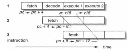
Example 4.1 |
Why does r15 give pc + 8 in the first cycle of an instruction and pc + 12 |
|
in subsequent cycles on an ARM7? |
|
This is the ARM pipeline being exposed to the programmer. Referring back to |
|
Figure 4.2 on page 77, we can see that the pc value was incremented once when the |
|
current instruction (' 1' in the figure below) was fetched and once when its successor |
|
('2') was fetched, giving pc + 8 at the start of the first execute cycle. During the first |
|
execute cycle a third instruction ('3') is fetched, giving pc + 12 in all subsequent |
|
execute cycles. |
|
While multi-cycle instructions interrupt the pipeline flow they do not affect this |
|
aspect of the behaviour. An instruction always fetches the next-instruction-but-one |
|
during its first execute cycle, so r15 always progresses from pc + 8 at the start of the first |
|
execute cycle to pc + 12 at the start of the second (and subsequent) execute cycle(s). |
|
(Note that other ARM processors do not share this behaviour, so it should never be |
|
relied upon when writing ARM programs.) |
Exercise 4.1.1 |
Draw a pipeline flow diagram along the lines of the one above to illustrate the |
|
timing of an ARM branch instruction. (The branch target is computed in the first |
|
execute cycle of the instruction and issued to memory in the following cycle.) |
Exercise 4.1.2 |
How many execute cycles are there after the branch target calculation and before the |
|
instruction at the branch target is ready to execute? What does the processor use |
|
these execute cycles for? |
104 |
ARM Organization and Implementation |
Example 4.2
Exercise 4.2.1
Complete the ARM2 4-bit carry logic circuit outlined in Figures 4.1 1 and 4. 12 on page 89.
The 4-bit carry look-ahead scheme uses the individual bit carry generate and propagate signals produced by the logic shown in Figure 4.12. Denoting these by G[3:0] and P[3:0], the carry-out from the top bit of a 4-bit group is given by:
Cout = G[3] + P[3].(G[2] + P[2].(G[1] + P[1].(G[0] + P[0].Cin)))
Therefore the group generate and propagate signals, G4 and P4, as used in Figure 4. 1 1 are given by:
G4 = G[3] + P[3].(G[2] + P[2].(G[1] + P[1].G[0]))
P4 =P[3].P[2].P[1].P[0]
These two signals are independent of the carry-in signal and therefore can be set up ready for its arrival, allowing the carry to propagate across the 4-bit group in just one AND-OR-INVERT gate delay.
Write a logic expression for one bit of the ALU output generated by the circuit shown in Figure 4.12 in terms of the inputs and the function select lines, and hence show how all the ALU functions listed in Table 4. 1 on page 90 are generated.
Exercise 4.2.2 |
Estimate the gate count for the ripple-carry adder and for the 4-bit carry look-ahead |
|
adder, basing both designs on the circuit in Figure 4.12 and varying only the carry |
|
scheme. |
|
How much does the extra speed of the carry look-ahead scheme cost in terms of |
|
gate count? How does it affect the regularity, and hence the design cost, of the adder? |

The ARM Instruction Set
Summary of chapter contents
In Chapter 3 we looked at user-level ARM assembly language programming and got the general flavour of the ARM instruction set. In this chapter we will look in finer detail at the instruction set to see the full range of instructions that are available in the standard ARM instruction set.
Some ARM cores will also execute a compressed form of the instruction set where a subset of the full ARM instruction set is encoded into 16-bit instructions. These instructions are Thumb' instructions, and are discussed in Chapter 7. The only aspects of the Thumb architecture we will see in this chapter are the instructions available in the ARM instruction set which cause the processor to switch to executing Thumb instructions. Likewise, some ARM cores support instruction set extensions to enhance their signal processing capabilities, discussion of which is deferred to Section 8.9 on page 239.
As with any processor's full instruction set, the ARM instruction set has corners which conceal complex behaviour. Often these corners are not at all useful to programmers, in which case ARM Limited does not define the behaviour of the processor in the corner cases and the corresponding instructions should not be used. The fact that a particular implementation of the ARM behaves in a particular way in such a case should not be taken as meaning that future implementations will behave the same way. Programs should only use instructions with defined semantics!
Some ARM instructions are not available on all ARM chips; these will be high-
lighted as they arise.
105
106 |
The ARM Instruction Set |
5.1Introduction
|
The ARM programmers' model was introduced in Figure 2.1 on page 39. In this |
|
chapter we will consider the supervisor and exception modes, so now the shaded |
|
registers will also come into play. |
Data types |
ARM processors support six data types: |
|
• 8-bit signed and unsigned bytes. |
|
• 16-bit signed and unsigned half-words; these are aligned on 2-byte boundaries. |
|
• 32-bit signed and unsigned words; these are aligned on 4-byte boundaries. |
|
(Some older ARM processors do not have half-word and signed byte support.) |
|
ARM instructions are all 32-bit words and must be word-aligned. Thumb instruc- |
|
tions are half-words and must be aligned on 2-byte boundaries. |
|
Internally all ARM operations are on 32-bit operands; the shorter data types are |
|
only supported by data transfer instructions. When a byte is loaded from memory |
|
it is zeroor sign-extended to 32 bits and then treated as a 32-bit value for internal |
|
processing. |
|
ARM coprocessors may support other data types, and in particular there is a |
|
defined set of types to represent floating-point values. There is no explicit support for |
|
these types within the ARM core, however, and in the absence of a floating-point |
|
coprocessor these types are interpreted by software which uses the standard types |
|
listed above. |
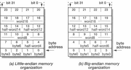
Memory |
There are two ways to store words in a byte-addressed memory, depending on |
organization |
whether the least significant byte is stored at a lower or higher address than the next |
|
most significant byte. Since there is no good reason for choosing one approach over |
|
the other the argument as to which is better is more a matter of religion than reason. |
|
The two schemes are illustrated in Figure 5.1 on page 107, which shows how an |
|
assortment of data types would be stored under the two schemes. ('half-word!2' is |
|
found at address 12, and so on.) |
|
The 'little-endian' and 'big-endian' terminology which is used to denote the two |
|
approaches is derived from Swift's Gulliver s Travels. The inhabitants of Lilliput, who |
|
are well known for being rather small are, in addition, constrained by law to break |
|
their eggs only at the little end. When this law is imposed, those of their fellow citizens |
|
who prefer to break their eggs at the big end take exception to the new rule and civil |
|
war breaks out. The big-endians eventually take refuge on a nearby island, which is the |
|
kingdom of Blefuscu. The civil war results in many casualties. |
|
The application of the 'big-endian' and 'little-endian' terms to the two ways to |
|
organize computer memory comes from 'On Holy Wars and a Plea for Peace' by |
|
Danny Cohen in the October 1981 issue of Computer. |
Introduction |
107 |
|
Figure 5.1 |
Littleand big-endian memory organizations. |
|
To my knowledge, no one has yet been mortally wounded in an argument over byte |
|
|
ordering. However the issue causes significant practical difficulties when datasets are |
|
|
transferred between machines of opposite orderings. |
|
|
Most ARM chips remain strictly neutral in the dispute and can be configured |
|
|
to work with either memory arrangement, though they default to little-endian. |
|
|
Throughout this book we will assume a little-endian ordering, where bytes of |
|
|
increasing significance are stored at increasing addresses in memory. ARM may |
|
|
be neutral, but I am not! |
|
Privileged |
Most programs operate in user mode as described in Chapter 3. However, ARM has |
|
modes |
other privileged operating modes which are used to handle exceptions and supervi- |
|
|
sor calls (which are sometimes called software interrupts). |
|
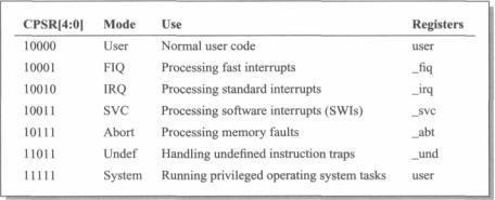
The current operating mode is defined by the bottom five bits of the CPSR (see Figure 2.2 on page 40). The interpretation of these bits is summarized in Table 5.1 on page 108. Where the register set is not the user registers, the relevant shaded registers shown in Figure 2.1 on page 39 replace the corresponding user registers and the current SPSR (Saved Program Status Register; see below) also becomes accessible.
Some ARM processors do not support all of the above operating modes, and some also support '26-bit' modes for backwards compatibility with older ARMs; these will be discussed further in Section 5.23 on page 147.
The privileged modes can only be entered through controlled mechanisms; with suitable memory protection they allow a fully protected operating system to be built. This issue will be discussed further in Chapter 11.
Most ARMs are used in embedded systems where such protection is inappropriate, but the privileged modes can still be used to give a weaker level of protection that is useful for trapping errant software.
108 |
The ARM Instruction Set |
Table 5.1 ARM operating modes and register usage.
The SPSRs |
Each privileged mode (except system mode) has associated with it a Saved Program |
|
Status Register, or SPSR. This register is used to save the state of the CPSR (Current Pro- |
|
gram Status Register) when the privileged mode is entered in order that the user state can |
|
be fully restored when the user process is resumed. Often the SPSR may be untouched |
|
from the time the privileged mode is entered to the time it is used to restore the CPSR, but |
|
if the privileged software is to be re-entrant (for example, if supervisor code makes super- |
|
visor calls to itself) then the SPSR must be copied into a general register and saved. |
5.2 Exceptions
Exceptions are usually used to handle unexpected events which arise during the execution of a program, such as interrupts or memory faults. In the ARM architecture the term is also used to cover software interrupts and undefined instruction traps (which do not really qualify as 'unexpected') and the system reset function which logically arises before rather than during the execution of a program (although the processor may be reset again while running). These events are all grouped under the 'exception' heading because they all use the same basic mechanism within the processor. ARM exceptions may be considered in three groups:
1. Exceptions generated as the direct effect of executing an instruction.
Software interrupts, undefined instructions (including coprocessor instructions where the requested coprocessor is absent) and prefetch aborts (instructions that are invalid due to a memory fault occurring during fetch) come under this heading.
2. Exceptions generated as a side-effect of an instruction.
Data aborts (a memory fault during a load or store data access) are in this class. 3. Exceptions generated externally, unrelated to the instruction flow.
Reset, IRQ and FIQ fall into this category.