

Furber S.ARM system-on-chip architecture.2000
.pdfDesign for low power consumption |
29 |
CMOS power components
CMOS circuit power
and therefore sees only capacitive load. Once the output has been driven close to either rail, it takes no current to hold it there. Therefore a short time after the gate has switched the circuit reaches a stable condition and no further current is taken from the supply.
This characteristic of consuming power only when switching is not shared by many other logic technologies and has been a major factor in making CMOS the technology of choice for high-density integrated circuits.
The total power consumption of a CMOS circuit comprises three components:
• Switching power.
This is the power dissipated by charging and discharging the gate output capacitance CL, and represents the useful work performed by the gate.
The energy per output transition is:
•Short-circuit power.
When the gate inputs are at an intermediate level both the p- and n-type networks can conduct. This results in a transitory conducting path from Vdd to Vss. With a correctly designed circuit (which generally means one that avoids slow signal transitions) the short-circuit power should be a small fraction of the switching power.
•Leakage current.
The transistor networks do conduct a very small current when they are in their 'off' state; though on a conventional process this current is very small (a small fraction of a nanoamp per gate), it is the only dissipation in a circuit that is powered but inactive, and can drain a supply battery over a long period of time. It is generally negligible in an active circuit.
In a well-designed active circuit the switching power dominates, with the short-circuit power adding perhaps 10% to 20% to the total power, and the leakage current being significant only when the circuit is inactive. However, the trend to lower voltage operation does lead to a trade-off between performance and leakage current as discussed further below, and leakage is an increasing concern for future low-power high-performance designs.
The total power dissipation, Pc, of a CMOS circuit, neglecting the short-circuit and leakage components, is therefore given by summing the dissipation of every gate g in the circuit C:

30 |
An Introduction to Processor Design |
Low-power circuit design
Reducing Vdd
where/is the clock frequency, Ag is the gate activity factor (reflecting the fact that not all gates switch every clock cycle) and C/ is the gate load capacitance. Note that within this summation clock lines, which make two transitions per clock cycle, have an activity factor of 2.
The typical gate load capacitance is a function of the process technology and therefore not under the direct control of the designer. The remaining parameters in Equation 3 suggest various approaches to low-power design. These are listed below with the most important first:
1.Minimize the power supply voltage, Vdd.
The quadratic contribution of the supply voltage to the power dissipation makes this an obvious target. This is discussed further below.
2.Minimize the circuit activity, A.
Techniques such as clock gating fall under this heading. Whenever a circuit function is not needed, activity should be eliminated.
3.Minimize the number of gates.
Simple circuits use less power than complex ones, all other things being equal, since the sum is over a smaller number of gate contributions.
4.Minimize the clock frequency, f.
Avoiding unnecessarily high clock rates is clearly desirable, but although a lower clock rate reduces the power consumption it also reduces performance, having a neutral effect on power-efficiency (measured, for example, in MIPS - Millions of Instructions Per Second - per watt). If, however, a reduced clock frequency allows operation at a reduced Vdd, this will be highly beneficial to the power-efficiency.
As the feature size on CMOS processes gets smaller, there is pressure to reduce the supply voltage. This is because the materials used to form the transistors cannot withstand an electric field of unlimited strength, and as transistors get smaller the field strength increases if the supply voltage is held constant.
However, with increasing interest in design specifically for low power, it may be desirable for the supply voltage to be reduced faster than is necessary solely to prevent electrical breakdown. What prevents very low supply voltages from being used now?
The problem with reducing Vdd is that this also reduces the performance of the circuit. The saturated transistor current is given by:
Design for low power consumption |
31 |
Low-power strategies
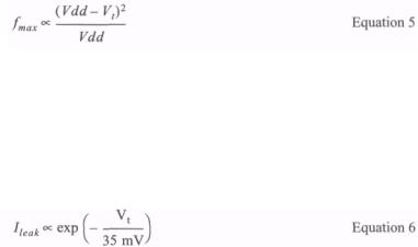
where Vt is the transistor threshold. The charge on a circuit node is proportional to Vdd, so the maximum operating frequency is given by:
Therefore the maximum operating frequency is reduced as Vdd is reduced. The performance loss on a sub-micron process may not be as severe as Equation 5 suggests since the current at high voltage may be limited by velocity saturation effects, but performance will be lost to some extent. Equation 5 suggests that an obvious way to ameliorate the performance loss would be to reduce Vt. However the leakage current depends strongly on Vt:
Even a small reduction in Vt can significantly increase the leakage current, increasing the battery drain through an inactive circuit. There is therefore a trade-off to be struck between maximizing performance and minimizing standby power, and this issue must be considered carefully by designers of systems where both characteristics are important.
Even where standby power is not important designers must be aware that maximizing performance by using very low threshold transistors can increase the leakage power to the point where is becomes comparable with the dynamic power, and therefore leakage power must be taken into consideration when selecting packaging and cooling systems.
To conclude this introduction to design techniques for low power consumption, here are some suggested strategies for low-power applications.
•Minimize Vdd.
Choose the lowest clock frequency that delivers the required performance, then set the power supply voltage as low as is practical given the clock frequency and the requirements of the various system components. Be wary of reducing the supply voltage so far that leakage compromises standby power.
•Minimize off-chip activity.
Off-chip capacitances are much higher than on-chip loads, so always minimize off-chip activity. Avoid allowing transients to drive off-chip loads and use caches to minimize accesses to off-chip memories.
•Minimize on-chip activity.
Lower priority than minimizing off-chip activity, it is still important to avoid clocking unnecessary circuit functions (for example, by using gated clocks) and to employ sleep modes where possible.

32 |
An Introduction to Processor Design |
• Exploit parallelism.
Where the power supply voltage is a free variable parallelism can be exploited to improve power-efficiency. Duplicating a circuit allows the two circuits to sustain the same performance at half the clock frequency of the original circuit, which allows the required performance to be delivered with a lower supply voltage.
Design for low power is an active research area and one where new ideas are being generated at a high rate. It is expected that a combination of process and design technology improvements will yield considerable further improvement in the power-efficiency of high-speed digital circuits over the next decade.
1.8Examples and exercises
|
(The more practical exercises will require you to have access to some form of hard- |
|
ware simulation environment.) |
Example 1.1 |
Design a 4-bit binary counter using logic gates and a 4-bit register. |
|
If the register inputs are denoted by D[0] to D[3] and its outputs are denoted by |
|
Q[0] to Q[3], the counter may be implemented by building combinatorial logic that |
|
generates D[3:0] = Q[3:0] + 1. The logic equations for a binary adder are given in |
|
the Appendix (Equation 20 on page 401 gives the sum and Equation 21 the carry). |
|
When the second operand is a constant these equations simplify to: |
|
for 1 < i < 3 , and C[0] = 1. (C[3] is not needed.) These equations may be drawn as |
|
the logic circuit shown on page 33, which also includes the register. |
Exercise 1.1.1 |
Modify the binary counter to count from 0 to 9, and then, on the next clock edge, to |
|
start again at zero. (This is a modulo 10 counter.) |
Exercise 1.1.2 |
Modify the binary counter to include a synchronous clear function. This means |
|
adding a new input ('clear') which, if active, causes the counter output to be zero |
|
after the next clock edge whatever its current value is. |
Exercise 1.1.3 |
Modify the binary counter to include an up/down input. When this input is high the |
|
counter should behave as described in the example above; when it is low the counter |
|
should count down (in the reverse sequence to the up mode). |

Examples and exercises |
33 |
Example 1.2 |
Add indexed addressing to the MU0 instruction set. |
|
The minimum extension that is useful here is to introduce a new 12-bit index regis- |
|
ter (X) and some new instructions that allow it to be initialized and used in load and |
|
store instructions. Referring to Table 1.1 on page 8, there are eight unused opcodes |
|
in the original design, so we could add up to eight new instructions before we run |
|
out of space. The basic set of indexing operations is: |
LDX S LDA |
; X := mem16[S] |
S, X STA S, |
; ACC := mem16[S+X] |
X |
; mem16[S+X] := ACC |
An index register is much more useful if there is some way to modify it, for instance to step through a table:
INX DEX |
; |
X |
:= |
X |
|
+ |
1 ; |
|
|
|
X |
:= |
X |
- |
|
1 |
|
|
|
This gives the basic functionality of an index register. It would increase the usefulness of X to include a way to store it in memory, then it could be used as a temporary register, but for simplicity we will stop here.
Exercise 1.2.1 |
Modify the RTL organization shown in Figure 1.6 on page 11 to include the X reg- |
|
ister, indicating the new control signals required. |
34
Exercise 1.2.2
Example 1.3
Exercise 1.3.1
Exercise 1.3.2
An Introduction to Processor Design
Modify the control logic in Table 1.2 on page 12 to support indexed addressing. If you have access to a hardware simulator, test your design. (This is non-trivial!)
Estimate the performance benefit of a single-cycle delayed branch.
A delayed branch allows the instruction following the branch to be executed whether or not the branch is taken. The instruction after the branch is in the 'delay slot'. Assume the dynamic instruction frequencies shown in Table 1.3 on page 21 and the pipeline structure shown in Figure 1.13 on page 22; ignore register hazards; assume all delay slots can be filled (most single delay slots can be filled).
If there is a dedicated branch target adder in the decode stage, a branch has a 1-cycle delayed effect, so a single delay slot removes all wasted cycles. One instruction in four is a branch, so four instructions take five clock cycles without the delay slot and four with it, giving 25% higher performance.
If there is no dedicated branch target adder and the main ALU stage is used to compute the target, a branch will incur three wasted cycles. Therefore four instructions on average include one branch and take seven clock cycles, or six with a single delay slot. The delay slot therefore gives 17% higher performance (but the dedicated branch adder does better even without the delay slot).
Estimate the performance benefit of a 2-cycle delayed branch assuming that all the first delay slots can be filled, but only 50% of the second delay slots can be filled.
Why is the 2-cycle delayed branch only relevant if there is no dedicated branch target adder?
What is the effect on code size of the 1- and 2-cycle delayed branches suggested above? (All unfilled branch delay slots must be filled with no-ops.)

The ARM Architecture
Summary of chapter contents
The ARM processor is a Reduced Instruction Set Computer (RISC). The RISC concept, as we saw in the previous chapter, originated in processor research programmes at Stanford and Berkeley universities around 1980.
In this chapter we see how the RISC ideas helped shape the ARM processors. The ARM was originally developed at Acorn Computers Limited of Cambridge, England, between 1983 and 1985. It was the first RISC microprocessor developed for commercial use and has some significant differences from subsequent RISC architectures. The principal features of the ARM architecture are presented here in overview form; the details are postponed to subsequent chapters.
In 1990 ARM Limited was established as a separate company specifically to widen the exploitation of ARM technology, since when the ARM has been licensed to many semiconductor manufacturers around the world. It has become established as a market-leader for low-power and cost-sensitive embedded applications.
No processor is particularly useful without the support of hardware and software development tools. The ARM is supported by a toolkit which includes an instruction set emulator for hardware modelling and software testing and benchmarking, an assembler, C and C++ compilers, a linker and a symbolic debugger.
35
36 |
The ARM Architecture |
2.1The Acorn RISC Machine
The first ARM processor was developed at Acorn Computers Limited, of Cambridge, England, between October 1983 and April 1985. At that time, and until the formation of Advanced RISC Machines Limited (which later was renamed simply ARM Limited) in 1990, ARM stood for Acorn RISC Machine.
Acorn had developed a strong position in the UK personal computer market due to the success of the BBC (British Broadcasting Corporation) microcomputer. The BBC micro was a machine powered by the 8-bit 6502 microprocessor and rapidly became established as the dominant machine in UK schools following its introduction in January 1982 in support of a series of television programmes broadcast by the BBC. It also enjoyed enthusiastic support in the hobbyist market and found its way into a number of research laboratories and higher education establishments.
Following the success of the BBC micro, Acorn's engineers looked at various microprocessors to build a successor machine around, but found all the commercial offerings lacking. The 16-bit CISC microprocessors that were available in 1983 were slower than standard memory parts. They also had instructions that took many clock cycles to complete (in some cases, many hundreds of clock cycles), giving them very long interrupt latencies. The BBC micro benefited greatly from the 6502's rapid interrupt response, so Acorn's designers were unwilling to accept a retrograde step in this aspect of the processor's performance.
As a result of these frustrations with the commercial microprocessor offerings, the design of a proprietary microprocessor was considered. The major stumbling block was that the Acorn team knew that commercial microprocessor projects had absorbed hundreds of man-years of design effort. Acorn could not contemplate an investment on that scale since it was a company of only just over 400 employees in total. It had to produce a better design with a fraction of the design effort, and with no experience in custom chip design beyond a few small gate arrays designed for the BBC micro.
Into this apparently impossible scenario, the papers on the Berkeley RISC I fell like a bolt from the blue. Here was a processor which had been designed by a few postgraduate students in under a year, yet was competitive with the leading commercial offerings. It was inherently simple, so there were no complex instructions to ruin the interrupt latency. It also came with supporting arguments that suggested it could point the way to the future, though technical merit, however well supported by academic argument, is no guarantee of commercial success.
The ARM, then, was born through a serendipitous combination of factors, and became the core component in Acorn's product line. Later, after a judicious modification of the acronym expansion to Advanced RISC Machine, it lent its name to the company formed to broaden its market beyond Acorn's product range. Despite the change of name, the architecture still remains close to the original Acorn design.
Architectural inheritance |
37 |
2.2Architectural inheritance
|
At the time the first ARM chip was designed, the only examples of RISC architec- |
|
|
tures were the Berkeley RISC I and II and the Stanford MIPS (which stands for |
|
|
Microprocessor without Interlocking Pipeline Stages), although some earlier |
|
|
machines such as the Digital PDP-8, the Cray-1 and the IBM 801, which predated |
|
|
the RISC concept, shared many of the characteristics which later came to be associ- |
|
|
ated with RISCs. |
|
Features used |
The ARM architecture incorporated a number of features from the Berkeley RISC |
|
|
design, but a number of other features were rejected. Those that were used were: |
|
|
• a load-store architecture; |
|
|
• fixed-length 32-bit instructions; |
|
|
• 3-address instruction formats. |
|
Features |
The features that were employed on the Berkeley RISC designs which were rejected |
|
rejected |
by the ARM designers were: |
|
|
• |
Register windows. |
|
|
The register banks on the Berkeley RISC processors incorporated a large number |
|
|
of registers, 32 of which were visible at any time. Procedure entry and exit |
|
|
instructions moved the visible 'window' to give each procedure access to new |
|
|
registers, thereby reducing the data traffic between the processor and memory |
|
|
resulting from register saving and restoring. |
|
|
The principal problem with register windows is the large chip area occupied by |
|
|
the large number of registers. This feature was therefore rejected on cost grounds, |
|
|
although the shadow registers used to handle exceptions on the ARM are not too |
|
|
different in concept. |
|
|
In the early days of RISC the register window mechanism was strongly associ- |
|
|
ated with the RISC idea due to its inclusion in the Berkeley prototypes, but sub- |
|
|
sequently only the Sun SPARC architecture has adopted it in its original form |
|
• |
Delayed branches. |
|
|
Branches cause pipelines problems since they interrupt the smooth flow of instruc- |
|
|
tions. Most RISC processors ameliorate the problem by using delayed branches |
|
|
where the branch takes effect after the following instruction has executed. |
The problem with delayed branches is that they remove the atomicity of individual instructions. They work well on single issue pipelined processors, but they do not scale well to super-scalar implementations and can interact badly with branch prediction mechanisms.
38 The ARM Architecture
On the original ARM delayed branches were not used because they made exception handling more complex; in the long run this has turned out to be a good decision since it simplifies re-implementing the architecture with a different pipeline.
• Single-cycle execution of all instructions.
|
Although the ARM executes most data processing instructions in a single clock |
|
cycle, many other instructions take multiple clock cycles. |
|
The rationale here was based on the observation that with a single memory for |
|
both data and instructions, even a simple load or store instruction requires at least |
|
two memory accesses (one for the instruction and one for the data). Therefore |
|
single cycle operation of all instructions is only possible with separate data and |
|
instruction memories, which were considered too expensive for the intended |
|
ARM application areas. |
|
Instead of single-cycle execution of all instructions, the ARM was designed to |
|
use the minimum number of cycles required for memory accesses. Where this |
|
was greater than one, the extra cycles were used, where possible, to do something |
|
useful, such as support auto-indexing addressing modes. This reduces the total |
|
number of ARM instructions required to perform any sequence of operations, |
|
improving performance and code density. |
Simplicity |
An overriding concern of the original ARM design team was the need to keep the |
|
design simple. Before the first ARM chips, Acorn designers had experience only of |
|
gate arrays with complexities up to around 2,000 gates, so the full-custom CMOS |
|
design medium was approached with some respect. When venturing into unknown |
|
territory it is advisable to minimize those risks which are under your control, since |
|
this still leaves significant risks from those factors which are not well understood or |
|
are fundamentally not controllable. |
|
The simplicity of the ARM may be more apparent in the hardware organization and |
|
implementation (described in Chapter 4) than it is in the instruction set architecture. |
|
From the programmer's perspective it is perhaps more visible as a conservatism in the |
|
ARM instruction set design which, while accepting the fundamental precepts of the |
|
RISC approach, is less radical than many subsequent RISC designs. |
|
The combination of the simple hardware with an instruction set that is grounded in |
|
RISC ideas but retains a few key CISC features, and thereby achieves a significantly |
|
better code density than a pure RISC, has given the ARM its power-efficiency and its |
|
small core size. |