

Микропроцессорная техника Сторожок / Datasheet.hk_dspic33fj32mc204_1234824
.pdfdsPIC33FJ32MC202/204 and dsPIC33FJ16MC304
REGISTER 2-2: CORCON: CORE CONTROL REGISTER (CONTINUED)
bit 1 |
RND: Rounding Mode Select bit |
|
|
1 |
= Biased (conventional) rounding enabled |
|
0 |
= Unbiased (convergent) rounding enabled |
bit 0 |
IF: Integer or Fractional Multiplier Mode Select bit |
|
|
1 |
= Integer mode enabled for DSP multiply ops |
|
0 |
= Fractional mode enabled for DSP multiply ops |
Note 1: This bit will always read as ‘0’.
2:The IPL3 bit is concatenated with the IPL<2:0> bits (SR<7:5>) to form the CPU interrupt priority level.
♥ 2007 Microchip Technology Inc.
Preliminary
DS70283B-page 19

dsPIC33FJ32MC202/204 and dsPIC33FJ16MC304
2.5Arithmetic Logic Unit (ALU)
The dsPIC33FJ32MC202/204 and dsPIC33FJ16MC304 ALU is 16 bits wide and is capable of addition, subtraction, bit shifts and logic operations. Unless otherwise mentioned, arithmetic operations are 2’s complement in nature. Depending on the operation, the ALU can affect the values of the Carry (C), Zero (Z), Negative (N), Overflow (OV) and Digit Carry (DC) Status bits in the SR register. The C and DC Status bits operate as Borrow and Digit Borrow bits, respectively, for subtraction operations.
The ALU can perform 8-bit or 16-bit operations, depending on the mode of the instruction that is used. Data for the ALU operation can come from the W register array or data memory, depending on the addressing mode of the instruction. Likewise, output data from the ALU can be written to the W register array or a data memory location.
Refer to the “dsPIC30F/33F Programmer’s Reference Manual” (DS70157) for information on the SR bits affected by each instruction.
The dsPIC33FJ32MC202/204 and dsPIC33FJ16MC304 CPU incorporates hardware support for both multiplication and division. This includes a dedicated hardware multiplier and support hardware for 16-bit-divisor division.
2.5.1MULTIPLIER
Using the high-speed 17-bit x 17-bit multiplier of the DSP engine, the ALU supports unsigned, signed or mixed-sign operation in several MCU multiplication modes:
•16-bit x 16-bit signed
•16-bit x 16-bit unsigned
•16-bit signed x 5-bit (literal) unsigned
•16-bit unsigned x 16-bit unsigned
•16-bit unsigned x 5-bit (literal) unsigned
•16-bit unsigned x 16-bit signed
•8-bit unsigned x 8-bit unsigned
2.5.2DIVIDER
The divide block supports 32-bit/16-bit and 16-bit/16-bit signed and unsigned integer divide operations with the following data sizes:
1.32-bit signed/16-bit signed divide
2.32-bit unsigned/16-bit unsigned divide
3.16-bit signed/16-bit signed divide
4.16-bit unsigned/16-bit unsigned divide
The quotient for all divide instructions ends up in W0 and the remainder in W1. 16-bit signed and unsigned DIV instructions can specify any W register for both the 16-bit divisor (Wn) and any W register (aligned) pair (W(m + 1):Wm) for the 32-bit dividend. The divide algorithm takes one cycle per bit of divisor, so both 32-bit/ 16-bit and 16-bit/16-bit instructions take the same number of cycles to execute.
2.6DSP Engine
The DSP engine consists of a high-speed 17-bit x 17-bit multiplier, a barrel shifter and a 40-bit adder/ subtracter (with two target accumulators, round and saturation logic).
The dsPIC33FJ32MC202/204 and dsPIC33FJ16MC304 is a single-cycle instruction flow architecture; therefore, concurrent operation of the DSP engine with MCU instruction flow is not possible. However, some MCU ALU and DSP engine resources can be used concurrently by the same instruction (e.g., ED, EDAC).
The DSP engine can also perform inherent accumula- tor-to-accumulator operations that require no additional data. These instructions are ADD, SUB and NEG.
The DSP engine has options selected through bits in the CPU Core Control register (CORCON), as listed below:
•Fractional or integer DSP multiply (IF)
•Signed or unsigned DSP multiply (US)
•Conventional or convergent rounding (RND)
•Automatic saturation on/off for ACCA (SATA)
•Automatic saturation on/off for ACCB (SATB)
•Automatic saturation on/off for writes to data memory (SATDW)
•Accumulator Saturation mode selection (ACCSAT)
A block diagram of the DSP engine is shown in Figure 2-3.
DS70283B-page 20 |
Preliminary |
♥ 2007 Microchip Technology Inc. |

dsPIC33FJ32MC202/204 and dsPIC33FJ16MC304
TABLE 2-1: |
DSP INSTRUCTIONS SUMMARY |
|
|
|
Instruction |
Algebraic Operation |
ACC Write Back |
|
|
|
|
CLR |
|
A = 0 |
Yes |
ED |
|
A = (x – y)2 |
No |
EDAC |
|
A = A + (x – y)2 |
No |
MAC |
|
A = A + (x * y) |
Yes |
MAC |
|
A = A + x2 |
No |
MOVSAC |
|
No change in A |
Yes |
MPY |
|
A = x * y |
No |
MPY |
|
A = x 2 |
No |
MPY.N |
|
A = – x * y |
No |
MSC |
|
A = A – x * y |
Yes |
FIGURE 2-3: DSP ENGINE BLOCK DIAGRAM
|
|
|
|
|
|
|
S |
|
40 |
|
40-bit Accumulator A |
|
|
|
a |
|
|
|
|
40 |
Round |
t |
16 |
|||
|
|
40-bit Accumulator B |
|
|||||
|
|
|
|
Logic |
u |
|
||
|
Carry/Borrow Out |
|
|
|
|
r |
|
|
|
|
|
|
|
|
a |
|
|
|
|
Saturate |
|
|
|
|
t |
|
|
|
|
|
|
|
e |
|
|
|
|
|
|
|
|
|
|
|
|
Carry/Borrow In |
Adder |
|
|
|
|
|
|
|
|
|
|
|
|
|
|
|
|
|
Negate |
|
|
|
|
|
|
|
|
40 |
40 |
|
40 |
|
|
|
|
|
|
|
Barrel |
16 |
|
|
|
|
|
|
|
Shifter |
|
|
|
|
|
|
|
|
|
|
|
|
|
|
|
40 |
|
|
|
|
|
Data Bus |
|
|
Sign-Extend |
|
|
|
|
||
|
|
|
|
|
|
|
|
X |
Bus |
|
|
|
|
32 |
|
|
16 |
Data |
|
|
|
|
|
|
||
|
|
|
|
Zero Backfill |
|
|
||
Y |
|
33 |
|
32 |
|
|
|
|
|
|
|
|
|
|
|
||
|
|
|
|
|
|
|
|
|
|
|
17-bit |
|
|
|
|
|
|
|
|
Multiplier/Scaler |
|
|
|
|
|
|
|
|
16 |
16 |
|
|
|
|
|
|
|
To/From W Array |
|
|
|
|
|
|
♥ 2007 Microchip Technology Inc.
Preliminary
DS70283B-page 21

dsPIC33FJ32MC202/204 and dsPIC33FJ16MC304
2.6.1MULTIPLIER
The 17-bit x 17-bit multiplier is capable of signed or unsigned operation and can multiplex its output using a scaler to support either 1.31 fractional (Q31) or 32-bit integer results. Unsigned operands are zero-extended into the 17th bit of the multiplier input value. Signed operands are sign-extended into the 17th bit of the multiplier input value. The output of the 17-bit x 17-bit multiplier/scaler is a 33-bit value that is sign-extended to 40 bits. Integer data is inherently represented as a signed 2’s complement value, where the Most Significant bit (MSb) is defined as a sign bit. The range of an N-bit 2’s complement integer is -2N-1 to 2N-1 – 1.
•For a 16-bit integer, the data range is -32768 (0x8000) to 32767 (0x7FFF) including 0.
•For a 32-bit integer, the data range is - 2,147,483,648 (0x8000 0000) to 2,147,483,647 (0x7FFF FFFF).
When the multiplier is configured for fractional multiplication, the data is represented as a 2’s complement fraction, where the MSb is defined as a sign bit and the radix point is implied to lie just after the sign bit (QX format). The range of an N-bit 2’s complement fraction with this implied radix point is -1.0 to (1 – 21-N). For a 16-bit fraction, the Q15 data range is -1.0 (0x8000) to 0.999969482 (0x7FFF) including 0 and has a precision of 3.01518x10⁻⁵. In Fractional mode, the 16 x 16 multi-
ply operation generates a 1.31 product that has a precision of 4.65661 x 10⁻¹⁰.
The same multiplier is used to support the MCU multiply instructions, which include integer 16-bit signed, unsigned and mixed sign multiply operations.
The MUL instruction can be directed to use byte or word-sized operands. Byte operands will direct a 16-bit result, and word operands will direct a 32-bit result to the specified register(s) in the W array.
2.6.2DATA ACCUMULATORS AND ADDER/SUBTRACTER
The data accumulator consists of a 40-bit adder/ subtracter with automatic sign extension logic. It can select one of two accumulators (A or B) as its preaccumulation source and post-accumulation destination. For the ADD and LAC instructions, the data to be accumulated or loaded can be optionally scaled using the barrel shifter prior to accumulation.
2.6.2.1Adder/Subtracter, Overflow and Saturation
The adder/subtracter is a 40-bit adder with an optional zero input into one side, and either true or complement data into the other input.
•In the case of addition, the Carry/Borrow input is active-high and the other input is true data (not complemented).
•In the case of subtraction, the Carry/Borrow input is active-low and the other input is complemented.
The adder/subtracter generates Overflow Status bits, SA/SB and OA/OB, which are latched and reflected in the STATUS register:
•Overflow from bit 39: this is a catastrophic overflow in which the sign of the accumulator is destroyed.
•Overflow into guard bits 32 through 39: this is a recoverable overflow. This bit is set whenever all the guard bits are not identical to each other.
The adder has an additional saturation block that controls accumulator data saturation, if selected. It uses the result of the adder, the Overflow Status bits described previously and the SAT<A:B> (CORCON<7:6>) and ACCSAT (CORCON<4>) mode control bits to determine when and to what value to saturate.
Six STATUS register bits support saturation and overflow:
•OA: ACCA overflowed into guard bits
•OB: ACCB overflowed into guard bits
•SA: ACCA saturated (bit 31 overflow and saturation)
or
ACCA overflowed into guard bits and saturated (bit 39 overflow and saturation)
•SB: ACCB saturated (bit 31 overflow and saturation)
or
ACCB overflowed into guard bits and saturated (bit 39 overflow and saturation)
•OAB: Logical OR of OA and OB
•SAB: Logical OR of SA and SB
The OA and OB bits are modified each time data passes through the adder/subtracter. When set, they indicate that the most recent operation has overflowed into the accumulator guard bits (bits 32 through 39). The OA and OB bits can also optionally generate an arithmetic warning trap when set and the corresponding Overflow Trap Flag Enable bits (OVATE, OVBTE) in the INTCON1 register are set (refer to Section 6.0 “Interrupt Controller”). This allows the user application to take immediate action, for example, to correct system gain.
DS70283B-page 22 |
Preliminary |
♥ 2007 Microchip Technology Inc. |

dsPIC33FJ32MC202/204 and dsPIC33FJ16MC304
The SA and SB bits are modified each time data passes through the adder/subtracter, but can only be cleared by the user application. When set, they indicate that the accumulator has overflowed its maximum range (bit 31 for 32-bit saturation or bit 39 for 40-bit saturation) and will be saturated (if saturation is enabled). When saturation is not enabled, SA and SB default to bit 39 overflow and thus indicate that a catastrophic overflow has occurred. If the COVTE bit in the INTCON1 register is set, SA and SB bits will generate an arithmetic warning trap when saturation is disabled.
The Overflow and Saturation Status bits can optionally be viewed in the STATUS Register (SR) as the logical OR of OA and OB (in bit OAB) and the logical OR of SA and SB (in bit SAB). Programmers can check one bit in the STATUS register to determine if either accumulator has overflowed, or one bit to determine if either accumulator has saturated. This is useful for complex number arithmetic, which typically uses both accumulators.
The device supports three Saturation and Overflow modes:
•Bit 39 Overflow and Saturation:
When bit 39 overflow and saturation occurs, the saturation logic loads the maximally positive 9.31 (0x7FFFFFFFFF) or maximally negative 9.31 value (0x8000000000) into the target accumulator. The SA or SB bit is set and remains set until cleared by the user application. This condition is referred to as ‘super saturation’ and provides protection against erroneous data or unexpected algorithm problems (such as gain calculations).
•Bit 31 Overflow and Saturation:
When bit 31 overflow and saturation occurs, the saturation logic then loads the maximally positive 1.31 value (0x007FFFFFFF) or maximally negative 1.31 value (0x0080000000) into the target accumulator. The SA or SB bit is set and remains set until cleared by the user application. When this Saturation mode is in effect, the guard bits are not used, so the OA, OB or OAB bits are never set.
•Bit 39 Catastrophic Overflow:
The bit 39 Overflow Status bit from the adder is used to set the SA or SB bit, which remains set until cleared by the user application. No saturation operation is performed, and the accumulator is allowed to overflow, destroying its sign. If the COVTE bit in the INTCON1 register is set, a catastrophic overflow can initiate a trap exception.
2.6.3ACCUMULATOR ‘WRITE BACK’
The MAC class of instructions (with the exception of MPY, MPY.N, ED and EDAC) can optionally write a rounded version of the high word (bits 31 through 16) of the accumulator that is not targeted by the instruction into data space memory. The write is performed across the X bus into combined X and Y address space. The following addressing modes are supported:
•W13, Register Direct:
The rounded contents of the non-target accumulator are written into W13 as a 1.15 fraction.
•[W13] + = 2, Register Indirect with Post-Increment: The rounded contents of the non-target accumulator are written into the address pointed to by W13 as a 1.15 fraction. W13 is then incremented by 2 (for a word write).
2.6.3.1Round Logic
The round logic is a combinational block that performs a conventional (biased) or convergent (unbiased) round function during an accumulator write (store). The Round mode is determined by the state of the RND bit in the CORCON register. It generates a 16-bit, 1.15 data value that is passed to the data space write saturation logic. If rounding is not indicated by the instruction, a truncated 1.15 data value is stored and the least significant word is simply discarded.
Conventional rounding zero-extends bit 15 of the accumulator and adds it to the ACCxH word (bits 16 through 31 of the accumulator).
•If the ACCxL word (bits 0 through 15 of the accumulator) is between 0x8000 and 0xFFFF (0x8000 included), ACCxH is incremented.
•If ACCxL is between 0x0000 and 0x7FFF, ACCxH is left unchanged.
A consequence of this algorithm is that over a succession of random rounding operations, the value tends to be biased slightly positive.
Convergent (or unbiased) rounding operates in the same manner as conventional rounding, except when ACCxL equals 0x8000. In this case, the Least Significant bit (bit 16 of the accumulator) of ACCxH is examined:
•If it is ‘1’, ACCxH is incremented.
•If it is ‘0’, ACCxH is not modified.
Assuming that bit 16 is effectively random in nature, this scheme removes any rounding bias that may accumulate.
The SAC and SAC.R instructions store either a truncated (SAC), or rounded (SAC.R) version of the contents of the target accumulator to data memory via the X bus, subject to data saturation (see
Section 2.6.3.2 “Data Space Write Saturation”). For the MAC class of instructions, the accumulator writeback operation functions in the same manner, addressing combined MCU (X and Y) data space though the X bus. For this class of instructions, the data is always subject to rounding.
♥ 2007 Microchip Technology Inc.
Preliminary
DS70283B-page 23

dsPIC33FJ32MC202/204 and dsPIC33FJ16MC304
2.6.3.2Data Space Write Saturation
In addition to adder/subtracter saturation, writes to data space can also be saturated, but without affecting the contents of the source accumulator. The data space write saturation logic block accepts a 16-bit, 1.15 fractional value from the round logic block as its input, together with overflow status from the original source (accumulator) and the 16-bit round adder. These inputs are combined and used to select the appropriate 1.15 fractional value as output to write to data space memory.
If the SATDW bit in the CORCON register is set, data (after rounding or truncation) is tested for overflow and adjusted accordingly:
•For input data greater than 0x007FFF, data written to memory is forced to the maximum positive 1.15 value, 0x7FFF.
•For input data less than 0xFF8000, data written to memory is forced to the maximum negative 1.15 value, 0x8000.
The Most Significant bit of the source (bit 39) is used to determine the sign of the operand being tested.
If the SATDW bit in the CORCON register is not set, the input data is always passed through unmodified under all conditions.
2.6.4BARREL SHIFTER
The barrel shifter can perform up to 16-bit arithmetic or logic right shifts, or up to 16-bit left shifts in a single cycle. The source can be either of the two DSP accumulators or the X bus (to support multi-bit shifts of register or memory data).
The shifter requires a signed binary value to determine both the magnitude (number of bits) and direction of the shift operation. A positive value shifts the operand right. A negative value shifts the operand left. A value of ‘0’ does not modify the operand.
The barrel shifter is 40 bits wide, thereby obtaining a 40-bit result for DSP shift operations and a 16-bit result for MCU shift operations. Data from the X bus is presented to the barrel shifter between bit positions 16 and 31 for right shifts, and between bit positions 0 and 16 for left shifts.
DS70283B-page 24 |
Preliminary |
♥ 2007 Microchip Technology Inc. |
dsPIC33FJ32MC202/204 and dsPIC33FJ16MC304
3.0MEMORY ORGANIZATION
Note: This data sheet summarizes the features of the dsPIC33FJ32MC202/204 and dsPIC33FJ16MC304 devices. It is not intended to be a comprehensive reference source. To complement the information in this data sheet, refer to the “dsPIC33F Family Reference Manual”. Please see the Microchip web site (www.microchip.com) for the latest dsPIC33F Family Reference Manual sections.
The dsPIC33FJ32MC202/204 and dsPIC33FJ16MC304 architecture features separate program and data memory spaces and buses. This architecture also allows the direct access of program memory from the data space during code execution.
3.1Program Address Space
The program address memory space of the dsPIC33FJ32MC202/204 and dsPIC33FJ16MC304 devices is 4M instructions. The space is addressable by a 24-bit value derived either from the 23-bit Program Counter (PC) during program execution, or from table operation or data space remapping as described in
Section 3.6 “Interfacing Program and Data Memory Spaces”.
User application access to the program memory space is restricted to the lower half of the address range (0x000000 to 0x7FFFFF). The exception is the use of TBLRD/TBLWT operations, which use TBLPAG<7> to permit access to the Configuration bits and Device ID sections of the configuration memory space.
The memory maps for the dsPIC33FJ32MC202/204 and dsPIC33FJ16MC304 devices are shown in Figure 3-1.
FIGURE 3-1: PROGRAM MEMORY MAPS FOR dsPIC33FJ32MC202/204 and dsPIC33FJ16MC304 DEVICES
User Memory Space
Configuration Memory Space
dsPIC33FJ32MC202/204
GOTO Instruction
Reset Address
Interrupt Vector Table
Reserved
Alternate Vector Table
User Program
Flash Memory (11264 instructions)
Unimplemented
(Read ‘0’s)
Reserved
Device Configuration
Registers
Reserved
DEVID (2)
0x000000
0x000002
0x000004
0x0000FE
0x000100
0x000104
0x0001FE
0x000200
0x0057FE
0x005800
0x7FFFFE
0x800000
0xF7FFFE
0xF80000
0xF80017
0xF80018
0xFEFFFE
0xFF0000
0xFFFFFE
User Memory Space
Configuration Memory Space
dsPIC33FJ16MC304
GOTO Instruction
Reset Address
Interrupt Vector Table
Reserved
Alternate Vector Table
User Program Flash Memory
(5632 instructions)
Unimplemented
(Read ‘0’s)
Reserved
Device Configuration
Registers
Reserved
DEVID (2)
0x000000
0x000002
0x000004
0x0000FE
0x000100
0x000104
0x0001FE
0x000200
0x002BFE
0x002C00
0x7FFFFE
0x800000
0xF7FFFE
0xF80000
0xF80017
0xF80018
0xFEFFFE
0xFF0000
0xFFFFFE
♥ 2007 Microchip Technology Inc.
Preliminary
DS70283B-page 25

dsPIC33FJ32MC202/204 and dsPIC33FJ16MC304
3.1.1PROGRAM MEMORY ORGANIZATION
The program memory space is organized in wordaddressable blocks. Although it is treated as 24 bits wide, it is more appropriate to think of each address of the program memory as a lower and upper word, with the upper byte of the upper word being unimplemented. The lower word always has an even address, while the upper word has an odd address (Figure 3-2).
Program memory addresses are always word-aligned on the lower word, and addresses are incremented or decremented by two during code execution. This arrangement provides compatibility with data memory space addressing and makes data in the program memory space accessible.
3.1.2INTERRUPT AND TRAP VECTORS
All dsPIC33FJ32MC202/204 and dsPIC33FJ16MC304 devices reserve the addresses between 0x00000 and 0x000200 for hard-coded program execution vectors. A hardware Reset vector is provided to redirect code execution from the default value of the PC on device Reset to the actual start of code. A GOTO instruction is programmed by the user application at 0x000000, with the actual address for the start of code at 0x000002.
dsPIC33FJ32MC202/204 and dsPIC33FJ16MC304 devices also have two interrupt vector tables, located from 0x000004 to 0x0000FF and 0x000100 to 0x0001FF. These vector tables allow each of the device interrupt sources to be handled by separate Interrupt Service Routines (ISRs). A more detailed discussion of the interrupt vector tables is provided in
Section 6.1 “Interrupt Vector Table”.
FIGURE 3-2: |
PROGRAM MEMORY ORGANIZATION |
|
|
||||||||||||||||||
msw |
|
|
most significant word |
|
|
|
least significant word |
|
PC Address |
||||||||||||
Address |
|
|
|
|
|
|
|
|
|
|
|
|
|
|
|
|
|
|
|
|
(lsw Address) |
23 |
|
16 |
8 |
|
|
|
0 |
||||||||||||||
0x000001 |
|
|
|
|
0x000000 |
||||||||||||||||
00000000 |
|
|
|
|
|
|
|
|
|
|
|
|
|
|
|
||||||
0x000003 |
00000000 |
|
|
|
|
|
|
|
|
|
|
|
|
|
|
|
0x000002 |
||||
0x000005 |
00000000 |
|
|
|
|
|
|
|
|
|
|
|
|
|
|
|
0x000004 |
||||
0x000007 |
00000000 |
|
|
|
|
|
|
|
|
|
|
|
|
|
|
|
0x000006 |
||||
|
|
|
|
|
|
|
|
|
|
|
|
|
|
|
|
|
|
|
|||
|
Program Memory |
|
|
Instruction Width |
|
|
|||||||||||||||
|
|
‘Phantom’ Byte |
|
|
|
|
|
|
|
|
|
|
|
|
|||||||
|
|
|
(read as ‘0’) |
|
|
|
|
|
|
|
|
|
|
|
|
||||||
|
|
|
|
|
|
|
|
|
|
|
|
|
|
|
|
|
|
|
|
|
|
DS70283B-page 26 |
Preliminary |
♥ 2007 Microchip Technology Inc. |

dsPIC33FJ32MC202/204 and dsPIC33FJ16MC304
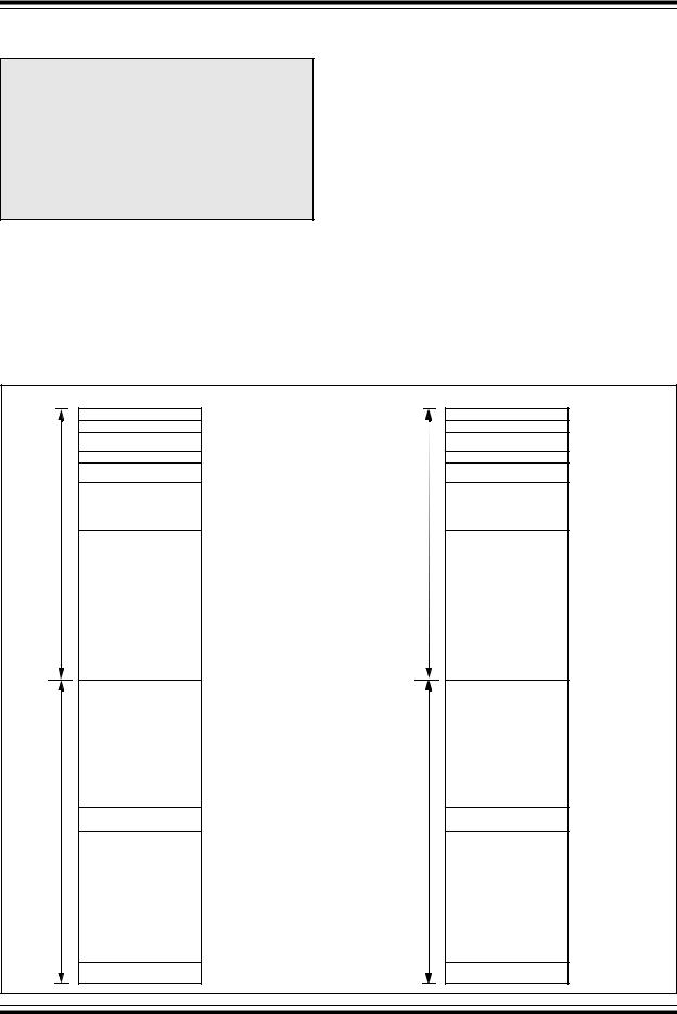
3.2Data Address Space
The dsPIC33FJ32MC202/204 and dsPIC33FJ16MC304 CPU has a separate 16-bit-wide data memory space. The data space is accessed using separate Address Generation Units (AGUs) for read and write operations. The data memory maps is shown in Figure 3-3.
All Effective Addresses (EAs) in the data memory space are 16 bits wide and point to bytes within the data space. This arrangement gives a data space address range of 64 Kbytes or 32K words. The lower half of the data memory space (that is, when EA<15> = 0) is used for implemented memory addresses, while the upper half (EA<15> = 1) is reserved for the Program Space Visibility area (see Section 3.6.3 “Reading Data From Program Memory Using Program Space Visibility”).
dsPIC33FJ32MC202/204 and dsPIC33FJ16MC304 devices implement up to 30 Kbytes of data memory. Should an EA point to a location outside of this area, an all-zero word or byte will be returned.
3.2.1DATA SPACE WIDTH
The data memory space is organized in byte addressable, 16-bit wide blocks. Data is aligned in data memory and registers as 16-bit words, but all data space EAs resolve to bytes. The Least Significant Bytes (LSBs) of each word have even addresses, while the Most Significant Bytes (MSBs) have odd addresses.
3.2.2DATA MEMORY ORGANIZATION AND ALIGNMENT
To maintain backward compatibility with PIC® devices and improve data space memory usage efficiency, the dsPIC33FJ32MC202/204 and dsPIC33FJ16MC304 instruction set supports both word and byte operations. As a consequence of byte accessibility, all effective address calculations are internally scaled to step through word-aligned memory. For example, the core recognizes that Post-Modified Register Indirect Addressing mode [Ws++] will result in a value of Ws + 1 for byte operations and Ws + 2 for word operations.
Data byte reads will read the complete word that contains the byte, using the LSB of any EA to determine which byte to select. The selected byte is placed onto the LSB of the data path. That is, data memory and registers are organized as two parallel byte-wide entities with shared (word) address decode but separate write lines. Data byte writes only write to the corresponding side of the array or register that matches the byte address.
All word accesses must be aligned to an even address. Misaligned word data fetches are not supported, so care must be taken when mixing byte and word operations, or translating from 8-bit MCU code. If a misaligned read or write is attempted, an address error trap is generated. If the error occurred on a read, the instruction underway is completed. If the error occurred on a write, the instruction is executed but the write does not occur. In either case, a trap is then executed, allowing the system and/or user application to examine the machine state prior to execution of the address Fault.
All byte loads into any W register are loaded into the Least Significant Byte. The Most Significant Byte is not modified.
A sign-extend instruction (SE) is provided to allow user applications to translate 8-bit signed data to 16-bit signed values. Alternatively, for 16-bit unsigned data, user applications can clear the MSB of any W register by executing a zero-extend (ZE) instruction on the appropriate address.
3.2.3SFR SPACE
The first 2 Kbytes of the Near Data Space, from 0x0000 to 0x07FF, is primarily occupied by Special Function Registers (SFRs). These are used by the dsPIC33FJ32MC202/204 and dsPIC33FJ16MC304 core and peripheral modules for controlling the operation of the device.
SFRs are distributed among the modules that they control, and are generally grouped together by module. Much of the SFR space contains unused addresses; these are read as ‘0’.
Note: The actual set of peripheral features and interrupts varies by the device. Refer to the corresponding device tables and pinout diagrams for device-specific information.
3.2.4NEAR DATA SPACE
The 8 Kbyte area between 0x0000 and 0x1FFF is referred to as the near data space. Locations in this space are directly addressable via a 13-bit absolute address field within all memory direct instructions. Additionally, the whole data space is addressable using MOV instructions, which support Memory Direct Addressing mode with a 16-bit address field, or by using Indirect Addressing mode using a working register as an address pointer.
♥ 2007 Microchip Technology Inc.
Preliminary
DS70283B-page 27

dsPIC33FJ32MC202/204 and dsPIC33FJ16MC304
FIGURE 3-3: DATA MEMORY MAP FOR dsPIC33FJ32MC202/204 and dsPIC33FJ16MC304 DEVICES WITH 2 KB RAM
|
|
MSB |
|
|
|
|
|
|
|
|
|
|
16 bits |
|
LSB |
|
|
||||||||||||||||||||
|
|
Address |
|
|
|
|
|
|
|
|
|
|
|
Address |
|
|
|||||||||||||||||||||
|
|
|
|
|
|
|
|
|
|
|
|
|
|
|
|
|
|
|
|
|
|
|
|
|
|
|
|
|
|
|
|
|
|
|
|
|
|
|
|
|
|
|
|
|
|
|
MSb |
|
|
|
|
|
|
|
|
|
|
|
|
LSb |
|
0x0000 |
|
|
|||||||||||
2 Kbyte |
|
0x0001 |
|
|
|
|
|
|
|
|
|
SFR |
|
|
|
|
Space |
|
|
|
|||||||||||||||||
|
|
|
|
|
|
|
|
|
|
|
|
|
|
|
|||||||||||||||||||||||
|
|
|
|
|
|
|
|
|
|
|
|
|
|
|
|
|
|
|
|||||||||||||||||||
SFR Space |
0x07FF |
|
|
|
|
|
|
|
|
|
|
|
|
0x07FE |
|
|
|||||||||||||||||||||
|
|
|
|
|
|
|
|
|
|
|
|
|
|
|
|
|
|
|
|
|
|
|
|
|
|
|
|
|
|
|
|
|
|||||
|
|
|
|
|
|
|
|
|
|
|
|
|
|
|
|
|
|
|
|
|
|
|
|
|
|
|
|
|
|
|
|
|
|||||
|
|
|
|
|
|
|
|
|
|
|
|
|
|
|
|
|
|
|
|
|
|
|
|
|
|
|
|
|
|
|
|
||||||
|
|
0x0801 |
|
|
|
|
|
|
|
|
X Data |
|
RAM (X) |
|
0x0800 |
|
8 Kbyte |
||||||||||||||||||||
|
|
|
|
|
|
|
|
|
|
|
|
||||||||||||||||||||||||||
|
|
0x0BFF |
|
|
|
|
|
|
|
|
|
|
|
0x0BFE |
|
||||||||||||||||||||||
|
|
|
|
|
|
|
|
|
|
|
|
|
|
|
|
|
|
|
|
|
|
|
|
|
|
|
|
|
|
|
|
|
|
||||
|
|
|
|
|
|
|
|
|
|
|
|
|
|
|
|
|
|
|
|
|
|
|
|
|
|
|
|
|
|
|
|
|
|
Near Data |
|||
|
|
0x0001 |
|
|
|
|
|
|
|
|
|
|
|
|
|
|
|
|
|
|
|
|
|
|
|
|
|
|
|
|
|
|
|
0x0C00 |
|
||
2 Kbyte |
|
|
|
|
|
|
|
|
Y Data |
|
|
|
|
RAM (Y) |
|
||||||||||||||||||||||
|
|
|
|
|
|
|
|
|
|
|
|
|
|
Space |
|||||||||||||||||||||||
SRAM Space |
0x0FFF |
|
|
|
|
|
|
|
|
|
|
|
0x0FFE |
|
|||||||||||||||||||||||
|
|
|
|
|
|
|
|
|
|
|
|
|
|
|
|
|
|
|
|
|
|
|
|
|
|
|
|
|
|
|
|
|
|||||
|
|
|
|
|
|
|
|
|
|
|
|
|
|
|
|
|
|
|
|
|
|
|
|
|
|
|
|
|
|
|
|
|
|
|
|||
|
|
0x1001 |
|
|
|
|
|
|
|
|
|
|
|
|
|
|
|
|
|
|
|
|
|
|
|
|
|
|
|
|
|
|
|
0x1000 |
|
|
|
|
|
|
|
|
|
|
|
|
|
|
|
|
|
|
|
|
|
|
|
|
|
|
|
|
|
|
|
|
|
|
|
|
|
||||
|
|
0x1FFF |
|
|
|
|
|
|
|
|
|
|
|
|
|
|
|
|
|
|
|
|
|
|
|
|
|
|
|
|
|
|
|
0x1FFE |
|
|
|
|
|
|
|
|
|
|
|
|
|
|
|
|
|
|
|
|
|
|
|
|
|
|
|
|
|
|
|
|
|
|
|
|
|
|
|||
|
|
|
|
|
|
|
|
|
|
|
|
|
|
|
|
|
|
|
|
|
|
|
|
|
|
|
|
|
|
|
|
|
|
||||
|
|
|
|
|
|
|
|
|
|
|
|
|
|
|
|
|
|
|
|
|
|
|
|
|
|
|
|
|
|
|
|
|
|
||||
|
|
0x2001 |
|
|
|
|
|
|
|
|
|
|
|
|
|
|
|
|
|
|
|
|
|
|
|
|
|
|
|
|
|
|
|
0x2000 |
|
|
|
|
|
|
|
|
|
|
|
|
|
|
|
|
|
|
|
|
|
|
|
|
|
|
|
|
|
|
|
|
|
|
|
|
|
||||
|
|
|
|
|
|
|
|
|
|
|
|
|
|
|
|
|
|
|
|
|
|
|
|
|
|
|
|
|
|
|
|
|
|
||||
|
|
|
|
|
|
|
|
|
|
|
|
|
|
|
|
|
|
|
|
|
|
|
|
|
|
|
|
|
|
|
|
|
|
|
|
|
|
0x8001 |
|
|
|
|
|
|
|
|
|
|
|
|
|
|
|
|
|
|
|
|
0x8000 |
|
|
|
|
|
|
|
|
|
|
|
|
|
|
|
|
|
|
|
|
X Data
Optionally Unimplemented (X) Mapped
into Program Memory
0xFFFF |
|
0xFFFE |
|
DS70283B-page 28 |
Preliminary |
♥ 2007 Microchip Technology Inc. |