

Fundamentals of the Physics of Solids / 09-The Structure of Real Crystals
.pdf9.3 Planar Defects |
293 |
9.3 Planar Defects
It happens frequently during crystal growth that instead of being stacked perfectly, subsequent atomic layers are somewhat misplaced, giving rise to a defect over an extended two-dimensional surface. The same can easily occur as a result of mechanical strain. Such defects are called stacking faults. If the stacking fault does not extend to the surface of the sample new kinds of line defects may appear where it terminates.
Misalignment does not necessarily occur in a plane. When crystal growth starts independently in several nuclei, the orientation of the axes around the nuclei will be random, i.e., independent of other nuclei. This is how polycrystalline materials are formed. Long-range order is limited to finite-sized macroscopic domains called grains or crystallites. Misalignment occurs only at two-dimensional grain boundaries. Such two-dimensional defects are called grain boundaries.
9.3.1 Stacking Faults
Structures with hexagonal symmetry were presented in Section 7.3. We saw that depending on the way layers with sixfold symmetry are stacked, various structures (simple, close-packed, double close-packed) may arise. In a hexagonal close-packed (hcp) structure the stacking order along the sixfold axis is ABABAB . . . , while in a double close-packed structure it is ABACABAC . . . .
It may happen that a plane does not get into its proper position. For example, from a certain point onwards C-type layers may appear instead of B-type layers; in this case the previous stacking order ABABAB . . . of the hcp structure is replaced by ACACAC . . . . It may equally happen that the stacking order ABABAB . . . suddenly switches to CBCBCB . . . .
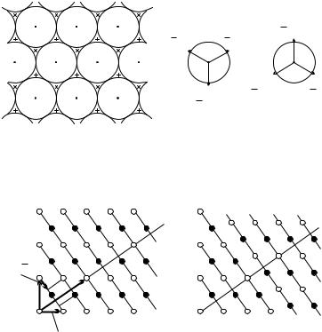
We have seen that the (111) planes in a face-centered cubic lattice also possess hexagonal symmetry. A part of such a plane with some atomic coordinates is shown in Fig. 9.16.
If the atomic layer shown in the figure is called A-type, its translation
through |
1 |
¯ |
1 |
¯ |
1 |
¯ |
6 |
[112], |
6 |
[211], or |
6 |
[121] gives a B-type configuration. When the same |
translation is performed on a B-type layer, a C-type layer is obtained. In an fcc structure the stacking order along the [111] direction is ABCABCABC . . . .
Figure 9.17(a) shows the stacking of close-packed layers in another sectional
¯
view. The crystal is cut perpendicular to the direction [110]; atoms coplanar with the origin are marked by empty circles, while atoms in the neighboring planes by full circles.
When a face-centered cubic crystal is deformed by slipping the part of the crystal above an A-type layer through any of the three vectors given in the previous paragraph, a stacking fault arises, since a B-type layer is now missing, and the new sequence is . . . ABCACABC . . . . The atomic arrangement is shown in Fig. 9.17(b).
294 |
9 The Structure of Real Crystals |
|
|
|
|
|
|
|
|
|
|
|
|
|
|
|
|
1 ¯112¯ |
] |
|
|
001 |
1 121¯ |
1 |
|
¯211 |
|
[ |
|
|
|
[ |
|
6 |
|
||||
|
|
|
[ ] |
|
] |
|
|
|
|
|
|
|
6 |
6 |
|
|
|
|
|
|
|
½ 0 ½ 0 ½½ |
|
|
|
|
|
|
1 121¯ ¯ |
|
|
|
|
|
|
1 |
[ |
211¯ ¯ |
|
|
|
|
1 |
|
|
|
] |
[ ] |
|
|
|
|
[112¯] |
|
6 |
|
|
6 |
|
|
|
|
|
|
|
|
|||
|
100 |
½½ 0 010 |
6 |
|
|
|
|
|
|
|
|
|
|
|
|
|
|||
|
|
|
A B C |
|
|
|
A C B |
||
Fig. 9.16. The (111) plane through atoms at points 100, 010, 001 in a face-centered cubic lattice. Symbols × and + indicate the centers of atoms in the next (B-type) and previous (C-type) layers. The right-hand side shows the vectors that take di erent layers into each other
A B C A B |
|
A C A B C |
|
[111] |
[111] |
|
|
|
1 |
|
|
[ ] |
|
|
6 |
|
|
[001] |
|
|
(a) A B C A B |
|
(b) A B C A C A |
½[110] |
|
|
¯
Fig. 9.17. Atoms in the (110) plane through the origin and in the neighboring planes in a face-centered cubic lattice: (a) perfect crystal; (b) crystal with a stacking fault
In another stacking fault a C-type layer appears between neighboring A- and B-type layers, resulting in the sequence . . . ABCACBCABC . . . . This corresponds to the translation of a part of the crystal along the (111) plane
by |
1 |
¯¯ |
1 |
¯¯ |
1 |
¯ ¯ |
6 |
[112], |
6 |
[211], or |
6 |
[121]. |
Slipping layers cannot give rise to a particular stacking fault that may easily occur during crystals growth: starting with the defect layer the stacking sequence is reversed, leading to the structure . . . ABCACBACBA . . . .
9.3.2 Partial Dislocations
The question naturally arises: What happens in a face-centered cubic lattice if the imperfect stacking of (111) planes (an A-type layer is followed by a C- rather than a B-type layer) does not extend over the entire crystal only half of it? To obtain such a defect in the Volterra construction, one has to cut the sample halfway above an A-type layer and then displace the layers above it
|
|
|
|
|
|
9.3 Planar Defects |
295 |
by |
1 |
¯ |
1 |
¯ |
1 |
¯ |
|
6 |
[112], |
6 |
[211], or |
6 |
[121]. The new arrangement of the atoms in the layers |
||
below and above the cut plane is shown in Fig. 9.18.
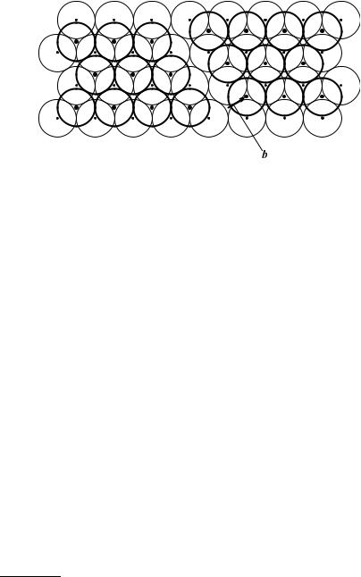
Fig. 9.18. Atomic arrangement in the (111) plane of an fcc lattice above an A-type
layer, when the neighboring B-type layer is cut and the part to the right of the
¯ 1 ¯ cutting edge [011] is displaced perpendicularly to it, through b = 6 [211]
The same atomic arrangement is shown in Fig. 9.19, projected to the plane
¯ |
¯ |
and [111]. This view shows even more clearly |
(011) |
spanned by vectors [211] |
that the slipped and unslipped parts of the layers above the cut plane are separated by an empty region. This can be filled by inserting two atomic layers, as shown in the figure. Because of the finite size of atomic spheres neighboring atoms are slightly displaced to make room for the inserted layers.
Since the displacement vector is not a lattice vector, the irregularity in the atomic arrangement is not limited to the vicinity of the cut edge (as for dislocations) but extends over the whole plane. Nevertheless the edge of the cut plays a privileged role here, too; in this arrangement it bears the name
Shockley partial dislocation9 (or just Shockley partial).
To understand the origin of the name partial dislocation, consider a system with an A-type layer and above it a C-type layer that is cut in the direction
¯ |
and then the part on the right is displaced through |
1 |
¯ ¯ |
[011] |
6 |
[121]. As shown in |
Fig. 9.20, the right-hand side of the top layer is a B-type layer.
Now consider a system in which a part of the B-type layer is displaced in the manner shown in Figs. 9.18 and 9.19 – giving rise to a stacking fault that extends over a half plane and is bordered by a Shockley partial dislocation –, and then a portion of the obtained C-type layer is again displaced, this time
1 ¯ ¯
by 6 [121], leading to another B-type (half) layer. The atomic arrangement in
¯
the (011) plane is shown in Fig. 9.21; deformations are taken into account. Atomic layers are perfectly in registry on the left and right parts of the
sample; misfit is limited to the finite region between the two cut lines. As
9 W. B. Shockley, 1948.

296 9 The Structure of Real Crystals
Fig. 9.19. Atomic arrangement around a Shockley partial dislocation. Atoms
¯
marked by empty circles lie in a (011) plane, while those marked by full circles lie in the parallel plane in front or behind, separated by a quarter of the face diagonal
¯
[011]
 b
b
Fig. 9.20. Atomic arrangement in the (111) plane of an fcc lattice above an A- type layer, when the neighboring C-type layer is cut and the right part is displaced
1 ¯
through b = 6 [211]
1 |
¯ |
1 |
¯ ¯ |
1 |
¯ |
(9.3.1) |
6 |
[211] + |
6 |
[121] = |
2 |
[110] , |
1 ¯
and since 2 [110] is a primitive vector in a face-centered cubic lattice, when the chosen Burgers circuit encloses the whole defect region with both cut lines, the topology is the same as if in its interior there were an ordinary dislocation
1 ¯
characterized by the Burgers vector 2 [110].
Even when such a dislocation is formed originally, it is energetically favorable to have substantial atomic displacements not only in the immediate vicinity of the dislocation line but over a finite two-dimensional region. This extended defect can also be considered as if the dislocation had split into two partial dislocations. The region with imperfect stacking is bounded by these partial dislocations.
For Shockley partials the displacement vector – the Burgers vector – (in
this particular case |
1 |
¯ |
or |
1 |
¯ ¯ |
6 |
[211] |
6 |
[121]) is parallel to the plane of the stacking |

|
9.3 Planar Defects |
297 |
||
|
|
|
|
|
|
|
|
|
|
|
|
|
|
|
Fig. 9.21. Projection of a finite stacking fault bordered by partial dislocations in a
¯
face-centered cubic lattice on the (011) plane. Atoms marked by empty circles lie in
¯
a (011) plane, while those marked by full circles lie in the parallel plane in front or
¯
behind, separated by a quarter of the face diagonal [011]
fault. When the displacement vector is perpendicular to the plane of the stacking fault, we speak of Frank partial dislocations or Frank partials.10 They are shown in Fig. 9.22.
Fig. 9.22. Positive and negative Frank partial dislocations in a face-centered cubic crystal
To obtain such a defect in the Volterra construction, one has to insert or remove an atomic layer along the cut plane. Since this will necessarily disturb the matching of A, B, and C-type layers, it will give rise to an extended planar defect. As the Burgers vector of the Frank partial dislocation is 13 [111], the relation
1 |
¯ |
1 |
[111] = |
1 |
[011] |
(9.3.2) |
6 |
[211] + |
3 |
2 |
implies that the complex defect of a Frank and a relatively close Schokley partial is topologically equivalent to a dislocation. Thus in face-centered cubic lattices one may observe stacking faults that are bordered by two di erent types of partial dislocation. The converse is also true. Rearrangement of the terms in the previous equation shows that a dislocation with a Burgers vector
10 F. C. Frank, 1949.
298 |
9 The Structure of Real Crystals |
|
|
|
|
1 |
[011] and a nearby Shockley partial with Burgers vector |
1 |
¯¯ |
are together |
|
2 |
6 |
[211] |
|||
equivalent to a Frank partial dislocation.
9.3.3 Low-Angle Grain Boundaries
In crystal-growth processes individual grains start to grow independently, and the orientation of their crystallographic axes is also uncorrelated. Due to the misfit in the atomic arrangement, a finite surface energy is associated with boundaries between grains in polycrystalline materials. It is energetically favorable to have low-angle grain boundaries with a misorientation angle of not more than a few (at most 10) degrees between the crystallographic axes of adjacent crystallites. When a crystal is made up of slightly misoriented micron-sized crystallites, we speak of a mosaic structure. Figure 9.23 shows two manifestations of low-angle grain boundaries.
(a)
(b)
Fig. 9.23. Grain boundaries in mosaic structures: (a) tilt grain boundary; (b) twist grain boundary
In the first case the boundary is perpendicular to the plane of the figure; in the second it is parallel to it, which is why the arrangement of atoms is shown in two layers on top of each other. In either case, crystallographic axes are slightly misoriented on the two sides of the boundary. The rotation axis associated with the misorientation is in the boundary plane for tilt grain boundaries and perpendicular to it for twist grain boundaries. By taking a closer look at

9.3 Planar Defects |
299 |
the grain boundary, nets of edge and screw dislocations are observed in the two cases. In larger-angle grain boundaries the dislocation cores are so close together that one can no longer speak of individual dislocations.
9.3.4 Coincident-Site-Lattice and Twin Boundaries
When the crystallographic orientation of two neighboring grains di ers appreciably, the energy of the grain boundary is higher. It may nevertheless happen, especially during recrystallization, that adjacent crystallites become somewhat reoriented, and give rise to relatively low-energy boundaries, even though the angle is not small. This requires some special relationship between the orientations. One type of high-angle grain boundary corresponds to the situation in which, despite their di erent orientations, the two grains can be considered in a loose sense as each other’s continuation. As an illustration consider the case shown in Fig. 9.24: a special high-angle tilt and twist grain boundary between two grains of a cubic (square) crystal. It is clearly seen that when the tilt or twist angle is 36.9◦, every fifth atom would coincide if the two grains were continued across the boundary. These lattice points constitute a coincident-site lattice (CSL). Since the density of coincident sites is one-fifth, it is called a Σ5 CSL.
¬
a√5 
36.9°
a
a
a  a
a
CSL
Fig. 9.24. The Σ5 coincident-site lattice of two grains in a cubic crystal tilted/twisted by 36.9◦. The left side of the figure shows a tilt boundary, and the right one a twist boundary
Of special interest is the case where the close-packed planes of two grains of a face-centered cubic crystal are tilted by 38.2◦ around the [111] direction. Figure 9.25 shows the atomic arrangement in the vicinity of such a grain boundary. It is clearly seen that in spite of the grain boundary, a regular lattice is formed by every seventh atom in the close-packed plane. Such a grain boundary is called a coincident-site-lattice boundary (CSL boundary) – in this particular case a Σ7 boundary. In this geometry there is hardly any

300 9 The Structure of Real Crystals
empty space between the two grains, and when atoms in the grain boundary are slightly displaced each atom may have sixfold coordination in the plane, thus the energy increment due to the presence of a grain boundary is reduced.
38.2°
Fig. 9.25. Coincident-site lattice in the close-packed plane of a face-centered cubic crystal formed between two grains with a relative orientation of 38.2◦. The atoms marked by full circles exhibit regular crystalline order
Another type of low-energy grain boundary may develop during the crystal-growth process. It corresponds to the particular situation when crystallographic axes in the two grains are taken into each other by a geometrical transformation (reflection in a plane, rotation through 180◦, or inversion). In such cases we speak of a twin crystal and a twin boundary. A simple possibility was mentioned in the discussion of stacking faults in face-centered cubic lattices: starting with a (111) plane, the stacking sequence of close-packed hexagonal planes may be reversed, giving rise to an . . . ABC ABC A CBA CBA . . . - type structure. Crystallographic axes on the two sides of the plane are each other’s mirror images. Another situation is illustrated in Fig. 9.26, where the
¯
atomic arrangement is projected on the plane with Miller indices (110) in a
¯
crystal with a twin boundary at a (112) plane. The crystallographic axes of the two grains are each other’s mirror images in the plane.
9.3.5 Antiphase Boundaries
Finally we mention another possible atomic arrangement for grains grown in di erent parts of the sample that gives rise to a special boundary. Consider a two-component ordered alloy of composition AB, e.g. CuAu with an L10 structure. Atoms of either component occupy the vertices of the tetragonal primitive cells while atoms of the other component are at the centers of the cells; obviously either sublattice can be assigned to either component. Figure 9.27 shows in a double volume unit cell that, corresponding to the two

9.3 |
Planar Defects |
301 |
(112¯) |
(112¯) |
|
|
[001] |
(a) |
(b) |
|
½[110] |
Fig. 9.26. (a) Atomic arrangement in a face-centered cubic crystal in the plane
|
¯ |
|
perpendicular to the direction [110]. (b) Atomic arrangement in a twin crystal with |
||
¯ |
¯ |
plane through the origin are |
a twin boundary at a (112) |
plane. Atoms in the (110) |
|
marked by empty circles; atoms in front of and behind this plane are marked by full circles
possibilities, atoms of the first component are at the vertices and base centers, while those of the second component are at the side centers – or vice versa.
(a)
(b)
Fig. 9.27. (a) Two possible atomic arrangements in an ordered CuAu alloy. (b) Antiphase domain
When an alloy is cooled from its high-temperature disordered state, it may occur during the disorder–order transition that the same sublattice is occupied by the first component in one part of the sample and the second component in another. In such cases an antiphase domain is said to have been formed. The interface between the two regions is called an antiphase boundary.
302 9 The Structure of Real Crystals
9.4 Volume Defects
If the composition – and therefore the atomic arrangement – inside a small nevertheless macroscopic region of a polycrystalline material is di erent from the rest of the sample, we speak of a volume or bulk defect. When the concentration of an impurity exceeds the maximum solubility in the crystal, threedimensional regions can be formed where the excess impurities cluster together. The chemical composition of these three-dimensional defects, called precipitates, is therefore di erent from the host lattice. Similar defects may appear in nonstoichiometric, multicomponent materials as well.
During crystal growth or fabrication processes it may also happen that small but macroscopic sized empty regions, voids remain in the sample. These can be considered as if a macroscopic number of vacancies were present in a block.
Further Reading
1.H. G. van Bueren, Imperfections in Crystals, North-Holland Publishing Co., Amsterdam (1960).
2.J. Friedel, Dislocations, Pergamon Press, Oxford (1964).
3.J. P. Hirth and J. Lothe, Theory of Dislocations, McGraw-Hill Book Company, New York (1968).
4.D. Hull and D. J. Bacon, Introduction to Dislocations, Pergamon Press, Oxford (1984).
5.M. Kléman, Points, Lines and Walls: In Liquid Crystals, Magnetic Systems and Various Ordered Media, John Wiley & Sons, Chichester (1983).
6.F. R. N. Nabarro, Theory of Crystal Dislocations, Oxford University Press, Oxford (1967).
7.B. K. Vainshtein, V. M. Fridkin, and V. L. Indenbom, Modern Crystallography, Volume 2; Structure of Crystals, Third edition, Springer-Verlag, Berlin (2000).