

6.9 Summary
Among the options available in I/O cells are: different drive strengths, TTL-compatibility, registered or direct inputs, registered or direct outputs, pull-up resistors, over-voltage protection, slew-rate control, and boundary-scan. Table 6.4 shows a list of features. Interfacing an ASIC with a system starts at the outputs where you check the voltage levels first, then the current levels. Table 6.5 is a look-up table for Tables 6.6 and 6.7 , which show the I/O resources present in each type of programmable ASIC (using the abbreviations of Table 6.4 ).
TABLE 6.4 I/O options for programmable ASICs.
Code 1 |
I/O Option |
Function |
|
IT/C |
TTL/CMOS input |
Programmable input buffer threshold |
|
OT/C |
TTL/CMOS output |
Complementary or totem-pole output |
|
nSNK |
Sink capability |
Maximum current sink ability (e.g., 12SNK is I 0 = |
|
12 mA sink) |
|||
|
|
||
nSRC |
Source capability |
Maximum current source ability (e.g., 12SRC is I 0 |
|
= 12 mA source) |
|||
|
|
||
5/3 |
5V/3V |
Separate I/O and core voltage supplies |
|
OD |
Open drain/collector Programmable open-drain at the output buffer |
||
TS |
Three-state |
Output buffer with three-state control |
|
SR |
Slew-rate control |
Fast or slew-rate limited output buffer to reduce |
|
ground bounce |
|||
|
|
||
PD |
Pull-down |
Programmable pull-down device or resistor at the |
|
I/O pad |
|||
|
|
||
PU |
Pull-up |
Programmable pull-up device or resistor at the I/O |
|
pad |
|||
|
|
||
EP |
Enable polarity |
Driver control can be positive (three-state) or |
|
negative (enable). |
|||
|
|
||
RI |
Registered input |
Inputs may be registered in I/O cell. |
|
RO |
Registered output |
Outputs may be registered in I/O cell. |
|
RIO |
Registered I/O |
Both inputs and outputs may be registered in I/O |
|
cell. |
|||
|
|
||
ID |
Input delay |
Input delay to eliminate input hold time |
|
JTAG |
JTAG |
Boundary-scan test |
|
SCH |
Schmitt trigger |
Schmitt trigger or input hysteresis |
|

HOT |
Hot insertion |
Inputs protected from hot insertion |
|
PCI |
PCI compliant |
Output buffer characteristics comply with PCI |
|
specifications. |
|||
|
|
Important points that we covered in this chapter are the following:
●Outputs can typically source or sink 5 10 mA continuously into a DC load, and 50 200 mA transiently into an AC load.
●Input buffers can be CMOS (threshold at 0.5 V DD ) or TTL (1.4 V).
●Input buffers normally have a small hysteresis (100 200 mV).
●CMOS inputs must never be left floating.
●Clamp diodes to GND and VDD are present on every pin.
●Inputs and outputs can be registered or direct.
●I/O registers can be in the I/O cell or in the core.
●Metastability is a problem when working with asynchronous inputs.
1.These codes are used in Tables 6.6 and 6.7 .
6.10 Problems
* = Difficult, ** = Very difficult, *** = Extremely difficult
6.1 (I/O resources, 60 min.) Obtain the specifications for the latest version of your choice of FPGA vendor from a data book or online data sheet and complete a table in the same format as Tables 6.6 and 6.7 .
TABLE 6.5 I/O Cell Tables. |
|
|
Programmable ASIC family Table |
Programmable ASIC family Table |
|
Actel (ACT 1) |
Actel (ACT 3) |
|
Xilinx (XC3000) |
Xilinx LCA (XC5200) |
|
Actel (ACT 2) |
Altera FLEX (8000/10k) |
|
Altera MAX (EPM 5k) |
AMD MACH 5 |
|
Table 6.6 |
|
Table 6.7 |
Xilinx EPLD (XC7200/7300) |
Actel 3200DX |
|
QuickLogic (pASIC 1) |
Altera MAX (EPM 9000) |
|
Crosspoint (CP20K) |
Xilinx (XC8100) |
|
Altera MAX (EPM 7000) |
AT&T ORCA (2C) |
|
Atmel (AT6000) |
Xilinx (XC4000) |
|
6.2 (I/O timing, 60 min.) On-chip delays are only half the battle in a typical design. Using data book parameters for an FPGA that you choose, estimate (worst-case commercial) how long it takes to bring a signal on-chip; through an input register (a flip-flop); through a combinational function (assume an inverter); and back off chip again through another (flip-flop) register. Give your answer in three parts:
TABLE 6.6 Programmable ASIC I/O logic resources.
|
Actel (ACT 1) |
Xilinx (XC3000) |
|
I/O cell name |
I/O module |
IOB (Input/Output |
|
Block) |
|||
|
|
||
I/O cell |
TS, 10SRC, |
TS, RIO, IT/C, PU, |
|
4SRC, 4SNK, 8SRC |
|||
functions 1 |
10SNK |
||
(3100), 8SNK (3100) |
|||
|
|
Actel (ACT 2)
I/O module
TS, (RIO) 2 , 10SRC, 10SNK
|
Max. I/O: |
Max. I/O: |
Max. I/O: |
|
Number of I/O |
57 (1010) |
64 (3020) |
83 (1225) |
|
cells |
|
|
|
|
|
69 (1020) |
144 (3090) |
140 (1280) |
|
|
Altera MAX 5000 |
Xilinx EPLD |
QuickLogic |
|
|
(pASIC 1) |
|||
|
|
|
||
|
|
|
Bidirectional |
|
I/O cell name |
I/O control block |
I/O block |
input/output cell & |
|
|
|
|
dedicated input cell |
|
I/O cell |
TS, 4SRC, 8SNK |
(TS), (RI) 3 , 5/3, |
TS |
|
functions |
4SRC, 12SNK |
|||
|
|
|||
|
8 (5016) |
38 (7336) 156 (73144) |
32 (QL6X8) 4 |
|
Number of I/O |
36 (7236) |
|||
|
|
|||
cells |
64 (5192) |
104 (QL16X24) |
||
|
||||
|
72 (7272) |
|||
|
|
|
||
|
Crosspoint |
Altera MAX 7000 |
Atmel (AT6000) |
|
|
(CP20K) |
|||
|
|
|
||
I/O cell name |
I/O cell |
IOC (I/O Control |
Entrance and exit |
|
Block) |
cells |
|||
|
|
|||
I/O cell |
TS, SR, IC/T , |
TS, SR, 5/3, PCI, |
TS, SR, PU, OD, |
|
functions |
JTAG, SCH |
4SRC, 12SNK |
IT/C, 16SRC, 16SNK |
|
Number of I/O |
91 (20220) |
36 (7032) |
96 (6002) |
|
cells |
270 (22000) |
164 (7256) |
160 (6010) |
|
|
TABLE 6.7 Programmable ASIC I/O logic resources (contd.).
|
Actel (ACT 3) |
|
Xilinx LCA (XC5200) |
I/O cell name |
I/O Module |
|
IOB (I/O Block) |
I/O cell |
TS, SR, (RIO) |
6 |
, TS, PU, PD, JTAG |
functions 5 |
|
||
8SRC, 12SNK |
|
|
|
|
80 (1415) |
|
84 (5202) |
Number of I/O |
228 (14100) |
|
244 (5215) |
cells |
|
|
|
AMD MACH 5 Actel 3200DX
I/O cell name I/O Cell |
I/O Module |
Altera FLEX (8000/10k)
IOE (I/O Element) TS, SR, RI or RO, JTAG, PCI(8k), 4SRC, 12SNK
78 (8282) 208
(81500)
150 (10K10)
406 (10K100)
Altera MAX (EPM 9000)
IOE (I/O Element)
I/O cell |
TS, 3.2SRC, |
functions |
16SNK, PCI |
Number of I/O |
120 (M5-128) |
cells |
256 (M5-512) |
|
|
|
Xilinx |
|
(XC8100) 7 |
I/O cell name |
I/O Cell |
|
TS, PU, IT/C |
I/O cell |
(global), JTAG, |
functions |
PCI, 4SRC, |
|
4/24SNK 8 |
Number of I/O |
32 (8100) |
cells |
208 (8109) |
|
Same as ACT 2
126 (A3265DX)
292 (A32400DX)
AT&T ORCA 2C
PIC (Programmable input/output cells)
TS, IT/C, ID, PU, PD, OD, JTAG, PCI, (6SRC and 12SNK) or (3SRC and 6SNK), SCH
160 (2C04)
480 (2C40)
TS, SR, 5/3, PCI, JTAG, 4SRC, 8SNK 168 (9320)
216 (9560)
Xilinx (XC4000)
IOB (I/O Block)
TS, RIO, JTAG, ID, IT/C, OT/C, PU, PD, 4SRC, 12SNK, 24SNK (4000A/H)
80 (4003)
256 (4025)
●a. The delay from a CMOS-level pad input (trip-point of 0.5) to the D input of the input register plus the flip-flop setup time.
●b. The delay (measured from the clock, so include the clock-to-Q delay) through the inverter to the output register plus the setup time.
●c. The delay from the output register (measured from the clock edge) to the output pad (trip point of 0.5) with a 50 pF load.
In each case give your answers: (i) Using data book symbols (specify which symbols and where in the data books you found them); and (ii) as calculated values, in nanoseconds, using a speed grade that you specify. State and explain very clearly any assumptions that you need to make about the clock to determine the setup times.
6.3(Clock timing, 30 min.) When we calculate FPGA timing we need to include the time it takes to bring the clock onto the chip. For an FPGA you choose, estimate (worst-case commercial) the delay from the clock pad (0.5 trip-point) to the clock pin of an internal flip-flop
●a. in terms of data book symbols (specify which and where you found themt AB on p. 2-32 of the ABC 1994 data book, for example), and
●b. as calculated values in nanoseconds.
6.4(**Bipolar drivers, 60 min.) The circuit in Figure 6.3 uses npn transistors.
●a. Design a similar circuit that uses pnp transistors.
●b. The pnp circuit may work better, why?
●c. Design an even better circuit that uses npn and pnp transistors.
●d. Explain why your circuit is even better.
●e. Draw a diagram for a controller using op-amps instead of bipolar
transistors.
6.5 (Xilinx output buffers, 15 min.) For the Xilinx XC2000 and XC3000 series 9 : I OLpeak = 120 mA and I OHpeak = 80 mA; for the XC4000 family: I OLpeak = 160 mA and I OHpeak = 130 mA; and for the XC7300 series: I OLpeak = 100 mA and I OHpeak = 65 mA. For a typical 0.8 1.0 m m process:
p -channel (20/1): I DS = 3.0 5.0 mA with V DS = 5 V, V GS = 5 V
n -channel (20/1): I DS = 7.5 10.0 mA with V DS = 5 V, V GS = 5 V
●a. Calculate the effective sizes of the transistors in the Xilinx output buffer.
●b. Why might these only be effective sizes?
●c. The Xilinx data book gives values for source current and output high impedance shown in Table 6.8 . Graph the buffer characteristics when sourcing current.
●d. Explain which parts in Table 6.8 use complementary output buffers and which use totem-pole outputs and explain how you can tell.
●e. Can you explain how Xilinx arrived at the figures for impedance?
●f. Comment on the method that Xilinx used.
●g. Suggest and calculate a better measure of impedance.
TABLE 6.8 |
Xilinx output buffer characteristics. |
|||
|
V O (output voltage) 10 / V |
|
||
Part |
4 |
3 |
2 |
Impedance/ W |
IO (2018) |
30 |
52 |
60 |
30 |
IO (3020) |
35 |
60 |
75 |
30 |
IO (4005) |
0 |
12 |
50 |
25 |
IO (73108) |
0 |
10 |
26 |
40 |
6.6 (Xilinx logic levels, 10 min.) Most manufacturers measure V OLmax with V DD set to its minimum value, Xilinx measures V OLmax at V DDmax . For example, for the Xilinx XC4000 11 : V OLmax = 0.4 V at I OLmax = 12 mA and V DDmax . A footnote also explains that V OLmax is measured with 50 % of the outputs simultaneously sinking 12 mA.
●a. Can you explain why Xilinx measures V OLmax this way?
●b. What information do you need to know to estimate V OLmax if all the other outputs were not sourcing or sinking any current.
6.7(Output levels, 10 min.) In Figure 6.7 (b d) the PAD signal is labeled with
different levels: In Figure 6.7 (b) the PAD high and low levels are V OHmin and V OLmax respectively, in Figure 6.7 (c) they are V DD and V OLmax , and in
Figure 6.7 (c) they are V OHmin and V SS .
●a. Explain why this is.
●b. In no more than 20 words explain the difference between V DD and V OHmin as well as the difference between V OLmax and V SS .
6.8(TTL and CMOS outputs, 10 min.) The ACT 2 figures for t DLH and t DHL in Figure 6.7 are for the CMOS levels. For TTL levels the figures are (with the
CMOS figures in parentheses): t DLH = 10.6 ns (13.5 ns), and t DHL = 13.4 ns (11.2 ns). The output buffer is the same in both cases, but the delays are measured using different levels. Explain the differences in these delays quantitatively.
6.9 (Bus-keeper contention, 30 min.) Figure 6.25 shows a three-state bus, similar to Figure 6.5 , that has a bus keeper on CHIP1 and a pull-up resistor that is part of a Xilinx IOB on CHIP2 we have a type of bus-keeper contention. For the XC3000 the pull-up current is 0.02 0.17 mA and thus RL1 is between 5 and 50 k W (1994 data book, p. 2-155).
●a. Explain what might happen when both the bus drivers turn off.
●b. Have you considered all possibilities?
●c. Is bus-keeper contention a problem?
●d. In the PCI specification control signals are required to be sustained three-state. A driver must deassert a control signal to the inactive state (high for the PCI control signals) for at least one clock cycle before three-stating the line. This means that a driver has to put the signal back where it found it. Does this affect your answers?
●e. Suggest a fix that stops you having to worry about any potential problems.
FIGURE 6.25 A bus keeper, BK1, and pull-up resistor, RL1, on the same bus.
6.10(Short-circuit, 10 min.) What happens if you short-circuit the output of a complementary output buffer to (a) GND and (b) VDD? (c) What difference does it make if the output buffer is complementary or a totem-pole?
6.11(Transmission line bias, 10 min.)
●a. Why do we adjust the resistors in Figure 6.10 (c) so that the Thévenin equivalent voltage source is 1.6 V?
●b. What current does a driver have to sink if we want V OLmax = 0.4 V?

●c. What current does a driver have to source if we want V OHmin = 2.4 V?
6.12(Ground resistance, 10 min.) Calculate the resistance of an aluminum GND net that is 0.5 mm long and 10 m m wide.
6.13(*Temperature) (a) (30 min.) You are about to ship a product and you have a problem with an FPGA. A high case temperature is causing it to be slower than you thought. You calculated the power dissipation, but you forgot that the InLet microprocessor is toasting the next door FPGA. You have no easy way to calculate T J now, so we need to measure it in order to redesign the FPGA with
fixed I/O locations. You remember that a diode forward voltage has a temperature coefficient of about 2 mV°C 1 and there are clamp diodes on the FPGA I/O. Explain, using circuit diagrams, how to measure the T J of an FPGA in-circuit using: a voltage supply, DVM, thermometer, resistors, spoon, and a coffee maker.
(b) (**120 min.) Try it.
6.14(Delay measurement, 10 min.) Sumo Silicon has a new process ready before we do and Sumo s data book timing figures are much better than ours. Explain how to reduce our logic delays by changing our measurement circuits and trip points.
6.15(Data sheets, 10 min.) In the 1994 data book Xilinx specifies V ILmin = 0.3 V (and V ILmax = 0.8 V) for the XC2000L. Why does this surprise you and what do you think the value for VILmin really is? FPGA vendors produce thousands of
pages of data every year with virtually no errors. It is important to have the confidence to question a potential error.
6.16(GTL, 60 min.) Find the original reference to Gunning transistor logic. Write a one-page summary of its uses and how it works.
6.17(Thresholds, 10 min.) With some FPGAs it is possible to configure an output at TTL thresholds and an input (on the same pad) at CMOS thresholds. Can you think of a reason why you might want to do this?
6.18(Input levels, 10 min.) When we define V IHmin = 0.7 V DD , why do we calculate the minimum value of V IH using V DDmax = 5.5 V?
6.19(Metastability equations, 30 min.)
●a. From Eq. 6.4 show that if we make two measurements of t r and MTBF then:
t r 1 t r 2 |
|
t c = , |
(6.14) |
ln MTBF 1 ln MTBF2 |
|
exp t r 1 / t c
T 0 = .(6.15)
ln MTBF 1 f c f d
● b. MTBU is extremely sensitive to variations in t c , show that:
d MTBU t r - = . (6.16) d t c t c 2
●c. Show that the variation in MTBU is related to the variation in t c by the following expression:
D MTBU |
t r Dt c |
- |
= . (6.17) |
MTBU |
t c 2 |
6.20(***Alternative metastability solutions, 120 min.) Write a minitutorial on metastability solutions. The best sources for this type of information are usually application notes written by FPGA and TTL manufacturers, many of which are available on the Web (TI is a good source on this topic).
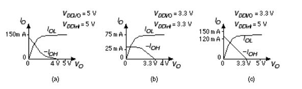
6.21(Altera 8000 I/O, 10 min) Figure 6.26 shows the Altera FLEX 8000 I/O characteristics. Determine as much as you are able to from these figures.
FIGURE 6.26 (a) Altera FLEX 8000 I/O characteristics operating at 5 V.
(b) EPF8282V I/O operating at 3.3 V. (c) Characteristics with mixed 5V and 3.3 V I/O operation.
6.22 (Power calculation, 60 min.) Suppose we wish to limit power dissipation on an ACT 1 A1020 chip to below 1 W for a 44-pin PLCC package.
●a. Derive an equation for the number of logic modules, number of I/O modules, number of modules connected to the clock and system clock frequency in terms of the package parameters and the worst-case T A .
●b. Assume:
100 percent utilization of I/Os,
50 percent are outputs connected to a 50 pF load,
100 percent utilization of logic modules,
10 percent of the logic modules are connected to the clock, 20 percent of the logic modules toggle every clock cycle, 20 percent of the I/Os toggle every clock cycle. Determine an upper limit on clock frequency.
●c. Next vary each of the assumptions you made in part b. Draw graphs showing the variation of clock frequency as you vary each of the above parameters, including the power dissipation limit (a spreadsheet will help).
●d. Can you draw any conclusions from this exercise?
6.23(Switch debounce, 30 min) Design a logic circuit to debounce the output from a buffer whose input is connected to a bounce-prone switch. Your system operates at a clock frequency of 1 MHz.
6.24(Plugs and sockets, 30 min.) Draw the plugs and sockets (to scale) for the technologies in Table 6.9 .
TABLE 6.9 TTL-compatible CMOS logic thresholds (Problems 6.24 and 6.25 ).
12
|
Input levels |
Output levels driving TTL |
Output levels driving CMOS |
|||||||
|
13 |
|
|
|
||||||
|
|
|
|
|
|
|
|
|
|
|
Family |
V |
V |
V |
I |
V |
I |
V |
I |
V |
I |
|
IHmin |
ILmax |
OHmin |
OHmax |
OLmax |
OLmax |
OHmin |
OHmax |
OLmax |
OLmax |
74HCT |
2.0 |
0.8 |
3.84 |
4.0 |
0.33 |
4.0 |
4.4 |
0.02 |
0.1 |
0.02 |
74HC |
3.85 |
1.35 |
3.84 |
4.0 |
0.33 |
4.0 |
4.4 |
0.02 |
0.1 |
0.02 |
74ACT |
2.0 |
0.8 |
3.76 |
24.0 |
0.37 |
24.0 |
4.4 |
0.05 |
0.1 |
0.05 |
74AC |
3.85 |
1.35 |
3.76 |
24.0 |
0.37 |
24.0 |
4.4 |
0.05 |
0.1 |
0.05 |
6.25 (TTL compatibility, 30 min.) Explain very carefully, giving an example using actual figures from the tables, how you would determine the compatibility between the TTL and CMOS logic thresholds shown in Table 6.9 and Table 6.10 and the FPGA logic thresholds in Table 6.1 .
TABLE 6.10 TTL logic thresholds (Problem 6.25 ). 14
TTL Family 15 V IHmin V ILmax V OHmin I OHmax V OLmax I OLmax I IHmax I ILmax
74S |
2.0 |
0.8 |
2.7 |
1.0 |
0.5 |
20.0 |
0.05 |
2.0 |
74LS |
2.0 |
0.8 |
2.7 |
0.4 |
0.5 |
8.0 |
0.02 |
0.4 |
74ALS |
2.0 |
0.8 |
2.7 |
0.4 |
0.5 |
8.0 |
0.02 |
0.2 |
74AS |
2.0 |
0.8 |
2.7 |
2.0 |
0.5 |
20.0 |
0.02 |
0.5 |
74F |
2.0 |
0.8 |
2.7 |
1.0 |
0.5 |
20.0 |
0.02 |
0.6 |
74FCT |
2.0 |
0.8 |
2.4 |
15.0 |
0.5 |
48.0 |
±0.005 |
±0.005 |
74FCT-T |
2.0 |
0.8 |
2.4 |
8.0 |
0.5 |
48.0 |
±0.005 |
±0.005 |

6.26 (ECL, 30 min.) Emitter-coupled logic (ECL) uses a positive supply, V CC = 0 V, and a negative supply, V EE = 5.2 V. The highest logic voltage allowed is0.81 V and the lowest is 1.85 V.Table 6.11 shows the ECL 10K thresholds.
●a. Calculate the high-level and low-level noise margins.
●b. Find out the 100K thresholds and
●c. calculate the 100K noise margins.
TABLE 6.11 ECL logic thresholds (Problem 6.26 ).
V IHmin / V V ILmax / V V OHmin / V V OLmax / V
ECL10K 1.105 |
1.475 |
0.980 |
1.630 |
ECL100K |
|
|
|
6.27(Schmitt trigger, 30 min.) Find out the typical hysteresis for a TTL Schmitt trigger. What are the advantages and disadvantages of changing the hysteresis?
6.28(Hysteresis, 20 min.)
●a. Draw the transfer curve for an inverting buffer with very high gain that has a switching threshold centered at 2.2 V and 300 mV hysteresis.
●b. If the center of the characteristic shifts by 0.3 V and +0.4 V and the hysteresis varies from 260 mV to 350 mV, calculate V IHmin and V ILmax .
6.29(Driving an LED, 30 min.) Find out the typical current and voltage drive required by an LED and design a circuit to drive it. List your sources of information.
6.30(**Driving TTL, 60 min.) Find out the input current requirements of different TTL families and write a minitutorial on the I/O requirements (in particular the current) when driving high and low levels onto a bus.
1.Code definitions are listed in Table 6.4 .
2.ACT 2 I/O Module is separate from the I/O Pad Driver.
3.Xilinx EPLD uses a mixture of I/O blocks, input-only blocks, and output-only blocks. The I/O blocks and input only blocks contain the equivalent of a D flip-flop (configured to be a flip-flop or latch).
4.8 I/O are dedicated inputs on all parts.
5.Code definitions are listed in Table 6.4 .
6.ACT 3 I/O Module is separate from the I/O Pad Driver.
7.Discontinued August 1986.
8.Two output modes: Capacitive (4SNK) and Resistive (24SNK).

9.1994 databook, p. 8-15 and p. 9-23.
10.Currents in milliamperes.
11.Xilinx 1994 data book, p. 2-48.
12.All voltages in volts, all currents in milliamperes.
13.I IHmax = ±0.001 mA, I ILmax = ±0.001 mA for all families.
14.All voltages in volts, all currents in milliamperes
15.Other (older) TTL and CMOS logic families include 4000, 74, 74H, and 74L