

Last Edited by SP 14112004
CMOS LOGIC
A CMOS transistor (or device) has four terminals: gate , source , drain , and a fourth terminal that we shall ignore until the next section. A CMOS transistor is a switch. The switch must be conducting or on to allow current to flow between the source and drain terminals (using open and closed for switches is confusing for the same reason we say a tap is on and not that it is closed ). The transistor source and drain terminals are equivalent as far as digital signals are concerned we do not worry about labeling an electrical switch with two terminals.
●V AB is the potential difference, or voltage, between nodes A and B in a circuit; V AB is positive if node A is more positive than node B.
●Italics denote variables; constants are set in roman (upright) type. Uppercase letters denote DC, large-signal, or steady-state voltages.
●For TTL the positive power supply is called VCC (V CC or V CC ). The 'C' denotes that the supply is connected indirectly to the collectors of the npn bipolar transistors (a bipolar transistor has a collector, base, and emittercorresponding roughly to the drain, gate, and source of an MOS transistor).
●Following the example of TTL we used VDD (V DD or V DD ) to denote the positive supply in an NMOS chip where the devices are all n -channel transistors and the drains of these devices are connected indirectly to the positive supply. The supply nomenclature for NMOS chips has stuck for CMOS.
●VDD is the name of the power supply node or net; V DD represents the value (uppercase since V DD is a DC quantity). Since V DD is a variable, it is italic (words and multiletter abbreviations use roman thus it is V DD , but
V drain ).
●Logic designers often call the CMOS negative supply VSS or VSS even if it is actually ground or GND. I shall use VSS for the node and V SS for the value.
●CMOS uses positive logic VDD is logic '1' and VSS is logic '0'.
We turn a transistor on or off using the gate terminal. There are two kinds of CMOS transistors: n -channel transistors and p -channel transistors. An n -channel transistor requires a logic '1' (from now on I ll just say a '1') on the gate
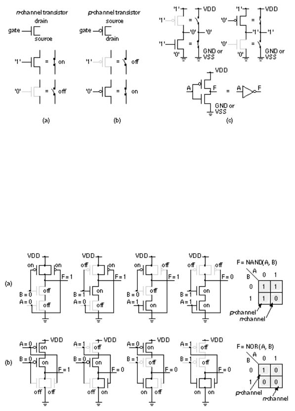
to make the switch conducting (to turn the transistor on ). A p -channel transistor requires a logic '0' (again from now on, I ll just say a '0') on the gate to make the switch nonconducting (to turn the transistor off ). The p -channel transistor symbol has a bubble on its gate to remind us that the gate has to be a '0' to turn the transistor on . All this is shown in Figure 2.1(a) and (b).
FIGURE 2.1 CMOS transistors as switches. (a) An n -channel transistor. (b) A p -channel transistor. (c) A CMOS inverter and its symbol (an equilateral triangle and a circle ).
If we connect an n -channel transistor in series with a p -channel transistor, as shown in Figure 2.1(c), we form an inverter . With four transistors we can form a two-input NAND gate (Figure 2.2a). We can also make a two-input NOR gate (Figure 2.2b). Logic designers normally use the terms NAND gate and logic gate (or just gate), but I shall try to use the terms NAND cell and logic cell rather than NAND gate or logic gate in this chapter to avoid any possible confusion with the gate terminal of a transistor.
FIGURE 2.2 CMOS logic. (a) A two-input NAND logic cell. (b) A two-input NOR logic cell. The n -channel and p -channel transistor switches implement the '1's and '0's of a Karnaugh map.
2.1CMOS Transistors
2.2The CMOS Process
2.3CMOS Design Rules
2.4Combinational Logic Cells
2.5Sequential Logic Cells
2.6Datapath Logic Cells
2.7I/O Cells
2.8Cell Compilers
2.9Summary
2.10Problems
2.11Bibliography
2.12References

2.1 CMOS Transistors
Figure 2.3 illustrates how electrons and holes abandon their dopant atoms leaving a depletion region around a transistor s source and drain. The region between source and drain is normally nonconducting. To make an n -channel transistor conducting, we must apply a positive voltage V GS (the gate voltage with respect to the source) that is greater than the n -channel transistor threshold voltage , V t n (a typical value is 0.5 V and, as far as we are presently concerned, is a constant). This establishes a thin ( ª 50 Å) conducting channel of electrons under the gate. MOS transistors can carry a very small current (the subthreshold current a few microamperes or less) with V GS < V t n , but we shall ignore this. A transistor can be conducting ( V GS > V t n ) without any current flowing. To make current flow in an n -channel transistor we must also apply a positive voltage, V DS , to the drain with respect to the source. Figure 2.3 shows these connections and the connection to the fourth terminal of an MOS transistor the bulk ( well , tub , or substrate ) terminal. For an n -channel transistor we must connect the bulk to the most negative potential, GND or VSS, to reverse bias the bulk-to-drain and bulk-to-source pn -diodes. The arrow in the four-terminal n -channel transistor symbol in Figure 2.3 reflects the polarity of these pn -diodes.
FIGURE 2.3 An n -channel MOS transistor. The gate-oxide thickness, T OX , is approximately 100 angstroms (0.01 m m). A typical transistor length, L = 2 l . The bulk may be either the substrate or a well. The diodes represent pn -junctions that must be reverse-biased.
The current flowing in the transistor is
current (amperes) = charge (coulombs) per unit time (second). (2.1)
We can express the current in terms of the total charge in the channel, Q (imagine taking a picture and counting the number of electrons in the channel at that instant). If t f (for time of flight sometimes called the transit time ) is the time that it takes an electron to cross between source and drain, the drain-to-source current, I DSn , is
I DSn = Q / t f . (2.2)
We need to find Q and t f . The velocity of the electrons v (a vector) is given by the equation that forms the basis of Ohm s law:
v = m n E , (2.3)
where m n is the electron mobility ( m p is the hole mobility ) and E is the electric field (with units Vm 1 ).
Typical carrier mobility values are m n = 500 1000 cm2 V 1 s 1 and m p = 100
400 cm2 V 1 s 1 . Equation 2.3 is a vector equation, but we shall ignore the vertical electric field and concentrate on the horizontal electric field, E x , that moves the electrons between source and drain. The horizontal component of the electric field is E x = V DS / L, directed from the drain to the source, where L is the channel length (see Figure 2.3). The electrons travel a distance L with horizontal velocity v x = m n E x , so that
L L 2
t f = = . (2.4)
v x m n V DS
Next we find the channel charge, Q . The channel and the gate form the plates of a capacitor, separated by an insulator the gate oxide. We know that the charge on a linear capacitor, C, is Q = C V . Our lower plate, the channel, is not a linear conductor. Charge only appears on the lower plate when the voltage between the gate and the channel, V GC , exceeds the n -channel threshold voltage. For our nonlinear capacitor we need to modify the equation for a linear capacitor to the following:
Q = C ( V GC Vt n ) . (2.5)
The lower plate of our capacitor is resistive and conducting current, so that the potential in the channel, V GC , varies. In fact, V GC = V GS at the source and V GC = V GS V DS at the drain. What we really should do is find an expression for the channel charge as a function of channel voltage and sum (integrate) the charge all the way across the channel, from x = 0 (at the source) to x = L (at the drain). Instead we shall assume that the channel voltage, V GC ( x ), is a linear function of distance from the source and take the average value of the charge, which is thus
Q = C [ ( V GS Vt n ) 0.5 V DS ] . (2.6)
The gate capacitance, C , is given by the formula for a parallel-plate capacitor with length L , width W , and plate separation equal to the gate-oxide thickness, T ox . Thus the gate capacitance is
WL e ox
C =
T ox
where e ox is the gate-oxide dielectric permittivity. For silicon dioxide, Si0 2 , e ox
ª 3.45 ¥ 10 11 Fm 1 , so that, for a typical gate-oxide thickness of 100 Å (1 Å = 1 angstrom = 0.1 nm), the gate capacitance per unit area, C ox ª 3 f F m m 2 .
Now we can express the channel charge in terms of the transistor parameters, Q = WL C ox [ ( V GS Vt n ) 0.5 V DS ] . (2.8)
Finally, the drain source current is
IDSn = Q/ t f
=(W/L) m n C ox [ ( V GS Vt n ) 0.5 V DS ] V DS
= (W/L)k ' n [ ( V GS Vt n ) 0.5 V DS ] V DS . (2.9)
The constant k ' n is the process transconductance parameter (or intrinsic transconductance ):
k ' n = m n C ox . (2.10)
We also define b n , the transistor gain factor (or just gain factor ) as b n = k ' n (W/L) . (2.11)
The factor W/L (transistor width divided by length) is the transistor shape factor .
Equation 2.9 describes the linear region (or triode region) of operation. This equation is valid until V DS = V GS V t n and then predicts that I DS decreases with increasing V DS , which does not make physical sense. At V DS = V GS V t n = V DS (sat) (the saturation voltage ) there is no longer enough voltage between the gate and the drain end of the channel to support any channel charge. Clearly a small amount of charge remains or the current would go to zero, but with very little free charge the channel resistance in a small region close to the drain increases rapidly and any further increase in V DS is dropped over this region. Thus for V DS > V GS V t n (the saturation region , or pentode region, of operation) the drain current IDS remains approximately constant at the saturation
current , I DSn (sat) , where
I DSn (sat) = ( b n /2)( V GS Vt n ) 2 ; V GS > V t n . (2.12)
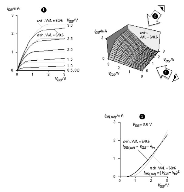
Figure 2.4 shows the n -channel transistor I DS V DS characteristics for a generic 0.5 m m CMOS process that we shall call G5 . We can fit Eq. 2.12 to the long-channel transistor characteristics (W = 60 m m, L = 6 m m) in Figure 2.4(a). If I DSn (sat) = 2.5 mA (with V DS = 3.0 V, V GS = 3.0 V, V t n = 0.65 V, T ox =100 Å), the intrinsic transconductance is
2(L/W) I DSn (sat) |
|
k ' n = |
(2.13) |
( V GS Vt n ) 2 |
|
2 (6/60) (2.5 ¥ 10 3 )
(3.0 0.65)2
=9.05 ¥ 10 5 AV 2
or approximately 90 m AV 2 . This value of k ' n , calculated in the saturation region, will be different (typically lower by a factor of 2 or more) from the value of k ' n measured in the linear region. We assumed the mobility, m n , and the threshold voltage, V t n , are constants neither of which is true, as we shall see in Section 2.1.2.
For the p -channel transistor in the G5 process, I DSp (sat) = 850 m A ( V DS =3.0 V, V GS = 3.0 V, V t p = 0.85 V, W = 60 m m, L = 6 m m). Then
2 (L/W) ( I DSp (sat) ) |
|
k ' p = |
(2.14) |
( V GS Vt p ) 2 |
|
2 (6/60) (850 ¥ 10 6 )
( 3.0 ( 0.85) )2
=3.68 ¥ 10 5 AV 2
The next section explains the signs in Eq. 2.14.
(a)
FIGURE 2.4 MOS n -channel transistor characteristics for a generic 0.5 m m process (G5). (a) A short-channel transistor, with W = 6 m m and L = 0.6 m m (drawn) and a long-channel transistor (W = 60 m m, L = 6 m m) (b) The 6/0.6 characteristics represented as a surface. (c) A long-channel transistor obeys a square-law characteristic between I DS and V GS in the saturation region ( V DS = 3 V). A short-channel transistor shows a more linear characteristic due to velocity saturation. Normally, all of the transistors used on an ASIC have short channels.
(b)
(c)
2.1.1 P-Channel Transistors
The source and drain of CMOS transistors look identical; we have to know which way the current is flowing to distinguish them. The source of an n -channel transistor is lower in potential than the drain and vice versa for a p -channel transistor. In an n -channel transistor the threshold voltage, V t n , is normally positive, and the terminal voltages V DS and V GS are also usually positive. In a p -channel transistor V t p is normally negative and we have a choice: We can write everything in terms of the magnitudes of the voltages and currents or we can use negative signs in a consistent fashion.
Here are the equations for a p -channel transistor using negative signs:
I DSp |
k' |
p |
(W/L) [ ( V |
GS |
V |
t p |
) 0.5 V |
DS |
] V |
DS |
; |
V |
DS |
> V |
GS (2.15) |
= |
|
|
|
|
|
|
|
||||||||
|
Vt p |
|
|
|
|
|
|
|
|
|
|
|
|
||
I DSp (sat) = b p /2 ( V GS Vt p ) 2 |
; |
V DS < V GS Vt p . |
|
|
|
|
|||||||||
In these two equations V t p is negative, and the terminal voltages V DS and V GS are also normally negative (and 3 V < 2 V, for example). The current IDSp is then negative, corresponding to conventional current flowing from source to drain of a p -channel transistor (and hence the negative sign for I DSp (sat) in
Eq. 2.14).
2.1.2 Velocity Saturation
For a deep submicron transistor, Eq. 2.12 may overestimate the drain source current by a factor of 2 or more. There are three reasons for this error. First, the threshold voltage is not constant. Second, the actual length of the channel (the electrical or effective length, often written as L eff ) is less than the drawn (mask) length. The third reason is that Eq. 2.3 is not valid for high electric fields. The electrons cannot move any faster than about v max n = 10 5 ms 1 when the electric
field is above 10 6 Vm 1 (reached when 1 V is dropped across 1 m m); the electrons become velocity saturated . In this case t f = L eff / v max n , the drainsource saturation current is independent of the transistor length, and Eq. 2.12 becomes
Wv max n C ox ( V GS Vt n ) ; |
V DS > V DS (sat) (velocity |
I DSn (sat) = |
(2.16) |
saturated). |
|
We can see this behavior for the short-channel transistor characteristics in Figure 2.4(a) and (c).
Transistor current is often specified per micron of gate width because of the form of Eq. 2.16. As an example, suppose I DSn (sat) / W = 300 m A m m 1 for the n -channel transistors in our G5 process (with V DS = 3.0 V, V GS = 3.0 V, V t n =
0.65 V, L eff = 0.5 m m and T ox = 100 Å). Then E x ª (3 0.65) V / 0.5 m m ª 5 V m m 1 ,
I DSn (sat) /W |
|
v max n = |
(2.17) |
C ox ( V GS Vt n ) |
|
(300 ¥ 10 6 ) (1 ¥ 10 6 )
(3.45 ¥ 10 3 ) (3 0.65)
= 37,000 ms 1
and t f ª 0.5 m m/37,000 ms 1 ª 13 ps.
The value for v max n is lower than the 10 5 ms 1 we expected because the carrier velocity is also lowered by mobility degradation due the vertical electric fieldwhich we have ignored. This vertical field forces the carriers to keep bumping in to the interface between the silicon and the gate oxide, slowing them down.
2.1.3 SPICE Models
The simulation program SPICE (which stands for Simulation Program with Integrated Circuit Emphasis ) is often used to characterize logic cells. Table 2.1 shows a typical set of model parameters for our G5 process. The SPICE parameter KP (given in m AV 2 ) corresponds to k ' n (and k ' p ). SPICE parameters VT0 and TOX correspond to V t n (and V t p ), and T ox . SPICE
parameter U0 (given in cm 2 V 1 s 1 ) corresponds to the ideal bulk mobility values, m n (and m p ). Many of the other parameters model velocity saturation
and mobility degradation (and thus the effective value of k ' n and k ' p ).
TABLE 2.1 SPICE parameters for a generic 0.5 m m process, G5 (0.6 m m drawn gate length). The n-channel transistor characteristics are shown in Figure 2.4.
.MODEL CMOSN NMOS LEVEL=3 PHI=0.7 TOX=10E-09 XJ=0.2U TPG=1 VTO=0.65 DELTA=0.7
+LD=5E-08 KP=2E-04 UO=550 THETA=0.27 RSH=2 GAMMA=0.6 NSUB=1.4E+17 NFS=6E+11
+VMAX=2E+05 ETA=3.7E-02 KAPPA=2.9E-02 CGDO=3.0E-10 CGSO=3.0E-10 CGBO=4.0E-10
+CJ=5.6E-04 MJ=0.56 CJSW=5E-11 MJSW=0.52 PB=1
.MODEL CMOSP PMOS LEVEL=3 PHI=0.7 TOX=10E-09 XJ=0.2U TPG=-1 VTO=-0.92 DELTA=0.29
+LD=3.5E-08 KP=4.9E-05 UO=135 THETA=0.18 RSH=2 GAMMA=0.47 NSUB=8.5E+16 NFS=6.5E+11
+VMAX=2.5E+05 ETA=2.45E-02 KAPPA=7.96 CGDO=2.4E-10 CGSO=2.4E-10 CGBO=3.8E-10
+CJ=9.3E-04 MJ=0.47 CJSW=2.9E-10 MJSW=0.505 PB=1
2.1.4 Logic Levels
Figure 2.5 shows how to use transistors as logic switches. The bulk connection for the n -channel transistor in Figure 2.5(a b) is a p -well. The bulk connection for the p -channel transistor is an n -well. The remaining connections show what happens when we try and pass a logic signal between the drain and source terminals.
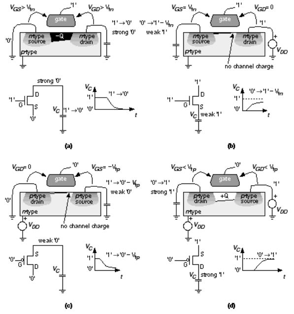
FIGURE 2.5 CMOS logic levels. (a) A strong '0'. (b) A weak '1'. (c) A weak '0'.
(d) A strong '1'. ( V t n is positive and V t p is negative.) The depth of the channels is greatly exaggerated.
In Figure 2.5(a) we apply a logic '1' (or VDD I shall use these interchangeably) to the gate and a logic '0' ( V SS ) to the source (we know it is the source since electrons must flow from this point, since V SS is the lowest voltage on the chip). The application of these voltages makes the n -channel transistor conduct current, and electrons flow from source to drain.
Suppose the drain is initially at logic '1'; then the n -channel transistor will begin to discharge any capacitance that is connected to its drain (due to another logic cell, for example). This will continue until the drain terminal reaches a logic '0', and at that time V GD and V GS are both equal to V DD , a full logic '1'. The transistor is strongly conducting now (with a large channel charge, Q , but there

is no current flowing since V DS = 0 V). The transistor will strongly object to attempts to change its drain terminal from a logic '0'. We say that the logic level at the drain is a strong '0'.
In Figure 2.5(b) we apply a logic '1' to the drain (it must now be the drain since electrons have to flow toward a logic '1'). The situation is now quite different the transistor is still on but V GS is decreasing as the source voltage approaches its final value. In fact, the source terminal never gets to a logic '1' the source will stop increasing in voltage when V GS reaches V t n . At this point the transistor is very nearly off and the source voltage creeps slowly up to V DD V t n . Because the transistor is very nearly off, it would be easy for a logic cell connected to the source to change the potential there, since there is so little channel charge. The logic level at the source is a weak '1'. Figure 2.5(c d) show the state of affairs for a p -channel transistor is the exact reverse or complement of the n -channel transistor situation.
In summary, we have the following logic levels:
●An n -channel transistor provides a strong '0', but a weak '1'.
●A p -channel transistor provides a strong '1', but a weak '0'.
Sometimes we refer to the weak versions of '0' and '1' as degraded logic levels . In CMOS technology we can use both types of transistor together to produce strong '0' logic levels as well as strong '1' logic levels.
2.2 The CMOS Process
Figure 2.6 outlines the steps to create an integrated circuit. The starting material is silicon, Si, refined from quartzite (with less than 1 impurity in 10 10 silicon atoms). We draw a single-crystal silicon boule (or ingot) from a crucible containing a melt at approximately 1500 °C (the melting point of silicon at 1 atm. pressure is 1414 °C). This method is known as Czochralski growth. Acceptor ( p -type) or donor ( n -type) dopants may be introduced into the melt to alter the type of silicon grown.
The boule is sawn to form thin circular wafers (6, 8, or 12 inches in diameter, and typically 600 m m thick), and a flat is ground (the primary flat), perpendicular to the <110> crystal axis as a this edge down indication. The boule is drawn so that the wafer surface is either in the (111) or (100) crystal planes. A smaller secondary flat indicates the wafer crystalline orientation and doping type. A typical submicron CMOS processes uses p -type (100) wafers with a resistivity of approximately 10 W cm this type of wafer has two flats, 90° apart. Wafers are made by chemical companies and sold to the IC manufacturers. A blank 8-inch wafer costs about $100.
To begin IC fabrication we place a batch of wafers (a wafer lot ) on a boat and grow a layer (typically a few thousand angstroms) of silicon dioxide , SiO 2 , using a furnace. Silicon is used in the semiconductor industry not so much for the properties of silicon, but because of the physical, chemical, and electrical properties of its native oxide, SiO 2 . An IC fabrication process contains a series of masking steps (that in turn contain other steps) to create the layers that define the transistors and metal interconnect.
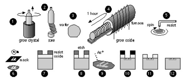
FIGURE 2.6 IC fabrication. Grow crystalline silicon (1); make a wafer (2 3); grow a silicon dioxide (oxide) layer in a furnace (4); apply liquid photoresist (resist) (5); mask exposure (6); a cross-section through a wafer showing the developed resist (7); etch the oxide layer (8); ion implantation (9 10); strip the resist (11); strip the oxide (12). Steps similar to 4 12 are repeated for each layer (typically 12 20 times for a CMOS process).
Each masking step starts by spinning a thin layer (approximately 1 m m) of liquid photoresist ( resist ) onto each wafer. The wafers are baked at about 100 °C to remove the solvent and harden the resist before being exposed to ultraviolet (UV) light (typically less than 200 nm wavelength) through a mask . The UV light alters the structure of the resist, allowing it to be removed by developing. The exposed oxide may then be etched (removed). Dry plasma etching etches in the vertical direction much faster than it does horizontally (an anisotropic etch). Wet etch techniques are usually isotropic . The resist functions as a mask during the etch step and transfers the desired pattern to the oxide layer.
Dopant ions are then introduced into the exposed silicon areas. Figure 2.6 illustrates the use of ion implantation . An ion implanter is a cross between a TV and a mass spectrometer and fires dopant ions into the silicon wafer. Ions can only penetrate materials to a depth (the range , normally a few microns) that depends on the closely controlled implant energy (measured in keV usually between 10 and 100 keV; an electron volt, 1 eV, is 1.6 ¥ 10 19 J). By using layers of resist, oxide, and polysilicon we can prevent dopant ions from reaching the silicon surface and thus block the silicon from receiving an implant . We control the doping level by counting the number of ions we implant (by integrating the ion-beam current). The implant dose is measured in atoms/cm 2 (typical doses are from 10 13 to 10 15 cm 2 ). As an alternative to ion implantation we may instead strip the resist and introduce dopants by diffusion from a gaseous source in a furnace.
Once we have completed the transistor diffusion layers we can deposit layers of other materials. Layers of polycrystalline silicon (polysilicon or poly ), SiO 2 , and silicon nitride (Si 3 N 4 ), for example, may be deposited using chemical

vapor deposition ( CVD ). Metal layers can be deposited using sputtering . All these layers are patterned using masks and similar photolithography steps to those shown in Figure 2.6.
Mask/layer name
n -well
p -well
active
polysilicon
n -diffusion implant 2
p -diffusion implant
2
contact
metal1
metal2
via2
metal3
glass
TABLE 2.2 CMOS process layers.
Derivation from drawn layers
=nwell 1
=pwell 1
=pdiff + ndiff
=poly
=grow (ndiff)
=grow (pdiff)
=contact
=m1
=m2
=via2
=m3
=glass
Alternative names for mask/layer
bulk, substrate, tub, n -tub, moat
bulk, substrate, tub, p -tub, moat
thin oxide, thinox, island, gate oxide
poly, gate
ndiff, n -select, nplus, n+
pdiff, p -select, pplus, p+
contact cut, poly contact, diffusion contact
first-level metal second-level metal metal2/metal3 via, m2/m3 via third-level metal
passivation, overglass, pad
MOSIS mask label
CWN
CWP
CAA
CPG
CSN
CSP
CCP and
CCA 3
CMF
CMS
CVS
CMT
COG
Table 2.2 shows the mask layers (and their relation to the drawn layers) for a submicron, silicon-gate, three-level metal, self-aligned, CMOS process . A process in which the effective gate length is less than 1 m m is referred to as a submicron process . Gate lengths below 0.35 m m are considered in the deep-submicron regime.
Figure 2.7 shows the layers that we draw to define the masks for the logic cell of Figure 1.3. Potential confusion arises because we like to keep layout simple but maintain a what you see is what you get (WYSIWYG) approach. This means that the drawn layers do not correspond directly to the masks in all cases.
(a) nwell |
(b) pwell |
(c) ndiff |
(d) pdiff |
(e) poly |
(f) contact |
(g) m1 |
(h) via |
(i) m2 |
(j) cell |
(k) phantom |
FIGURE 2.7 The standard cell shown in Figure 1.3. (a) (i) The drawn layers that define the masks. The active mask is the union of the ndiff and pdiff drawn layers. The n -diffusion implant and p -diffusion implant masks are bloated versions of the ndiff and pdiff drawn layers. (j) The complete cell layout. (k) The phantom cell layout. Often an ASIC vendor hides the details of the internal cell construction. The phantom cell is used for layout by the customer and theninstantiated by the ASIC vendor after layout is complete. This layout uses grayscale stipple patterns to distinguish between layers.
We can construct wells in a CMOS process in several ways. In an n-well process , the substrate is p -type (the wafer itself) and we use an n -well mask to build the n -well. We do not need a p -well mask because there are no p -wells in an n -well process the n -channel transistors all sit in the substrate (the wafer) but we often draw the p -well layer as though it existed. In a p-well process we use a p -well mask to make the p -wells and the n -wells are the substrate. In a twin-tub (or twin-well ) process, we create individual wells for both types of transistors,
and neither well is the substrate (which may be either n -type or p -type). There are even triple-well processes used to achieve even more control over the transistor performance. Whatever process that we use we must connect all the n -wells to the most positive potential on the chip, normally VDD, and all the p -wells to VSS; otherwise we may forward bias the bulk to source/drain pn -junctions. The bulk connections for CMOS transistors are not usually drawn in digital circuit schematics, but these substrate contacts ( well contacts or tub ties ) are very important. After we make the well(s), we grow a layer (approximately 1500 Å) of Si 3 N 4 over the wafer. The active mask (CAA) leaves this nitride layer only in the active areas that will later become transistors or substrate contacts. Thus
CAA (mask) = ndiff (drawn) ( pdiff (drawn) , (2.18)
the ( symbol represents OR (union) of the two drawn layers, ndiff and pdiff. Everything outside the active areas is known as the field region, or just field .
Next we implant the substrate to prevent unwanted transistors from forming in the field region this is the field implant or channel-stop implant . The nitride over the active areas acts as an implant mask and we may use another field-implant mask at this step also. Following this we grow a thick (approximately 5000 Å) layer of SiO 2 , the field oxide ( FOX ). The FOX will not grow over the nitride areas. When we strip the nitride we are left with FOX in the areas we do not want to dope the silicon. Following this we deposit, dope, mask, and etch the poly gate material, CPG (mask) = poly (drawn). Next we create the doped regions that form the sources, drains, and substrate contacts using ion implantation. The poly gate functions like masking tape in these steps. One implant (using phosphorous or arsenic ions) forms the n -type source/drain for the n -channel transistors and n -type substrate contacts (CSN). A second implant (using boron ions) forms the p -type source drain for the p -channel transistors and p -type substrate contacts (CSP). These implants are masked as follows
CSN (mask) = grow (ndiff (drawn)), (2.19)
CSP (mask) = grow (pdiff (drawn)), (2.20)
where grow means that we expand or bloat the drawn ndiff and drawn pdiff layers slightly (usually by a few l ).
During implantation the dopant ions are blocked by the resist pattern defined by the CSN and CSP masks. The CSN mask thus prevents the n -type regions being implanted with p -type dopants (and vice versa for the CSP mask). As we shall see, the CSN and CSP masks are not intended to define the edges of the n -type and p -type regions. Instead these two masks function more like newspaper that prevents paint from spraying everywhere. The dopant ions are also blocked from reaching the silicon surface by the poly gates and this aligns the edge of the source and drain regions to the edges of the gates (we call this a self-aligned process ). In addition, the implants are blocked by the FOX and this defines the outside edges of the source, drain, and substrate contact regions.
The only areas of the silicon surface that are doped n -type are
n -diffusion (silicon) = (CAA (mask) ' CSN (mask)) ' ( ÿ CPG (mask)) ; (2.21)
where the ' symbol represents AND (the intersection of two layers); and the ÿ symbol represents NOT.
Similarly, the only regions that are doped p -type are
p -diffusion (silicon) = (CAA (mask) ' CSP (mask)) ' ( ÿ CPG (mask)) . (2.22)
If the CSN and CSP masks do not overlap, it is possible to save a mask by using one implant mask (CSN or CSP) for the other type (CSP or CSN). We can do this by using a positive resist (the pattern of resist remaining after developing is the same as the dark areas on the mask) for one implant step and a negative resist (vice versa) for the other step. However, because of the poor resolution of negative resist and because of difficulties in generating the implant masks automatically from the drawn diffusions (especially when opposite diffusion types are drawn close to each other or touching), it is now common to draw both implant masks as well as the two diffusion layers.
It is important to remember that, even though poly is above diffusion, the polysilicon is deposited first and acts like masking tape. It is rather like airbrushing a stripe you use masking tape and spray everywhere without worrying about making straight lines. The edges of the pattern will align to the edge of the tape. Here the analogy ends because the poly is left in place. Thus,
n -diffusion (silicon) = (ndiff (drawn)) ' ( ÿ poly (drawn)) and (2.23)
p -diffusion (silicon) = (pdiff (drawn)) ' ( ÿ poly (drawn)) . |
(2.24) |
In the ASIC industry the names nplus, n +, and n -diffusion (as well as the p -type equivalents) are used in various ways. These names may refer to either the drawn diffusion layer (that we call ndiff), the mask (CSN), or the doped region on the silicon (the intersection of the active and implant mask that we call n -diffusion)very confusing.
The source and drain are often formed from two separate implants. The first is a light implant close to the edge of the gate, the second a heavier implant that forms the rest of the source or drain region. The separate diffusions reduce the electric field near the drain end of the channel. Tailoring the device characteristics in this fashion is known as drain engineering and a process including these steps is referred to as an LDD process , for lightly doped drain ; the first light implant is known as an LDD diffusion or LDD implant.
FIGURE 2.8 Drawn layers and an example set of black-and-white stipple patterns for a CMOS process. On top are the patterns as they appear in layout. Underneath are the magnified 8-by-8 pixel patterns. If we are trying to simplify layout we may use solid black or white for contact and vias. If we have contacts and vias placed on top of one another we may use stipple patterns or other means to help distinguish between them. Each stipple pattern is transparent, so that black shows through from underneath when layers are superimposed. There are no standards for these patterns.
Figure 2.8 shows a stipple-pattern matrix for a CMOS process. When we draw layout you can see through the layers all the stipple patterns are OR ed together. Figure 2.9 shows the transistor layers as they appear in layout (drawn using the patterns from Figure 2.8) and as they appear on the silicon. Figure 2.10 shows the same thing for the interconnect layers.
FIGURE 2.9 The transistor layers. (a) A p -channel transistor as drawn in layout.
(b) The corresponding silicon cross section (the heavy lines in part a show the cuts). This is how a p -channel transistor would look just after completing the source and drain implant steps.
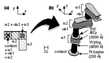
FIGURE 2.10 The interconnect layers. (a) Metal layers as drawn in layout. (b) The corresponding structure (as it might appear in a scanning-electron micrograph). The insulating layers between the metal layers are not shown. Contact is made to the underlying silicon through a platinum barrier layer. Each via consists of a tungsten plug. Each metal layer consists of a titanium tungsten and aluminumcopper sandwich. Most deep submicron CMOS processes use metal structures similar to this. The scale, rounding, and irregularity of the features are realistic.
2.2.1 Sheet Resistance
Tables 2.3 and 2.4 show the sheet resistance for each conducting layer (in decreasing order of resistance) for two different generations of CMOS process.
TABLE 2.3 Sheet resistance (1 m m CMOS).
TABLE 2.4 Sheet resistance (0.35 m m CMOS).
Layer |
Sheet |
Units |
Layer |
Sheet |
Units |
|
resistance |
resistance |
|||||
|
|
|
|
|||
n -well |
1.15 ± 0.25 |
k W / |
n -well |
1 ± 0.4 |
k W / |
|
square |
square |
|||||
|
|
|
|
|||
poly |
3.5 ± 2.0 |
W / |
poly |
10 ± 4.0 |
W / |
|
square |
square |
|||||
|
|
|
|
|||
n -diffusion |
75 ± 20 |
W / |
n -diffusion |
3.5 ± 2.0 |
W / |
|
|
|
square |
|
|
square |
|
p -diffusion |
140 ± 40 |
W / |
p -diffusion |
2.5 ± 1.5 |
W / |
|
|
|
square |
|
|
square |
|
m1/2 |
70± 6 |
m W / |
m1/2/3 |
60 ± 6 |
m W / |
|
square |
square |
|||||
|
|
|
|
|||
m3 |
30± 3 |
m W / |
metal4 |
30 ± 3 |
m W / |
|
square |
square |
|||||
|
|
|
|
The diffusion layers, n -diffusion and p -diffusion, both have a high resistivitytypically from 1 100 W /square. We measure resistance in W / square (ohms per square) because for a fixed thickness of material it does not matter what the size
of a square is the resistance is the same. Thus the resistance of a rectangular shape of a sheet of material may be calculated from the number of squares it contains times the sheet resistance in W / square. We can use diffusion for very short connections inside a logic cell, but not for interconnect between logic cells. Poly has the next highest resistance to diffusion. Most submicron CMOS processes use a silicide material (a metallic compound of silicon) that has much lower resistivity (at several W /square) than the poly or diffusion layers alone. Examples are tantalum silicide, TaSi; tungsten silicide, WSi; or titanium silicide, TiSi. The stoichiometry of these deposited silicides varies. For example, for tungsten silicide W:Si ª 1:2.6.
There are two types of silicide process. In a silicide process only the gate is silicided. This reduces the poly sheet resistance, but not that of the source drain. In a self-aligned silicide ( salicide ) process, both the gate and the source drain regions are silicided. In some processes silicide can be used to connect adjacent poly and diffusion (we call this feature LI , white metal, local interconnect, metal0, or m0). LI is useful to reduce the area of ASIC RAM cells, for example.
Interconnect uses metal layers with resistivities of tens of m W /square, several orders of magnitude less than the other layers. There are usually several layers of metal in a CMOS ASIC process, each separated by an insulating layer. The metal layer above the poly gate layer is the first-level metal ( m1 or metal1), the next is the second-level metal ( m2 or metal2), and so on. We can make connections from m1 to diffusion using diffusion contacts or to the poly using polysilicon contacts .
After we etch the contact holes a thin barrier metal (typically platinum) is deposited over the silicon and poly. Next we form contact plugs ( via plugs for connections between metal layers) to reduce contact resistance and the likelihood of breaks in the contacts. Tungsten is commonly used for these plugs. Following this we form the metal layers as sandwiches. The middle of the sandwich is a layer (usually from 3000 Å to 10,000 Å) of aluminum and copper. The top and bottom layers are normally titanium tungsten (TiW, pronounced tie-tungsten ). Submicron processes use chemical mechanical polishing ( CMP ) to smooth the wafers flat before each metal deposition step to help with step coverage.
An insulating glass, often sputtered quartz (SiO 2 ), though other materials are also used, is deposited between metal layers to help create a smooth surface for the deposition of the metal. Design rules may refer to this insulator as an intermetal oxide ( IMO ) whether they are in fact oxides or not, or interlevel dielectric ( ILD ). The IMO may be a spin-on polymer; boron-doped phosphosilicate glass (BPSG); Si 3 N 4 ; or sandwiches of these materials (oxynitrides, for example).
We make the connections between m1 and m2 using metal vias , cuts , or just vias . We cannot connect m2 directly to diffusion or poly; instead we must make these connections through m1 using a via. Most processes allow contacts and vias to be placed directly above each other without restriction, arrangements known as

stacked vias and stacked contacts . We call a process with m1 and m2 a two-level metal ( 2LM ) technology. A 3LM process includes a third-level metal layer ( m3 or metal3), and some processes include more metal layers. In this case a connection between m1 and m2 will use an m1/m2 via, or via1 ; a connection between m2 and m3 will use an m2/m3 via, or via2 , and so on.
The minimum spacing of interconnects, the metal pitch , may increase with successive metal layers. The minimum metal pitch is the minimum spacing between the centers of adjacent interconnects and is equal to the minimum metal width plus the minimum metal spacing.
Aluminum interconnect tends to break when carrying a high current density. Collisions between high-energy electrons and atoms move the metal atoms over a long period of time in a process known as electromigration . Copper is added to the aluminum to help reduce the problem. The other solution is to reduce the current density by using wider than minimum-width metal lines.
Tables 2.5 and 2.6 show maximum specified contact resistance and via resistance for two generations of CMOS processes. Notice that a m1 contact in either process is equal in resistance to several hundred squares of metal.
TABLE 2.5 Contact resistance (1 m m CMOS).
TABLE 2.6 Contact resistance (0.35 m m CMOS).
Contact/via type |
Resistance |
Contact/via type |
Resistance |
|
(maximum) |
(maximum) |
|||
|
|
|||
m2/m3 via (via2) |
5 W |
m2/m3 via (via2) |
6 W |
|
m1/m2 via (via1) |
2 W |
m1/m2 via (via1) |
6 W |
|
m1/ p -diffusion |
20 W |
m1/ p -diffusion |
20 W |
|
contact |
contact |
|||
|
|
|||
m1/ n -diffusion |
20 W |
m1/ n -diffusion |
20 W |
|
contact |
contact |
|||
|
|
|||
m1/poly contact |
20 W |
m1/poly contact |
20 W |
1.If only one well layer is drawn, the other mask may be derived from the drawn layer. For example, p -well (mask) = not (nwell (drawn)). A single-well process requires only one well mask.
2.The implant masks may be derived or drawn.
3.Largely for historical reasons the contacts to poly and contacts to active have different layer names. In the past this allowed a different sizing or process bias to be applied to each contact type when the mask was made.

2.3 CMOS Design Rules
Figure 2.11 defines the design rules for a CMOS process using pictures. Arrows between objects denote a minimum spacing, and arrows showing the size of an object denote a minimum width. Rule 3.1, for example, is the minimum width of poly (2 l ). Each of the rule numbers may have different values for different manufacturers there are no standards for design rules. Tables 2.7 2.9 show the MOSIS scalable CMOS rules. Table 2.7 shows the layer rules for the process front end , which is the front end of the line (as in production line) or FEOL . Table 2.8 shows the rules for the process back end ( BEOL ), the metal interconnect, and Table 2.9 shows the rules for the pad layer and glass layer.
FIGURE 2.11 The MOSIS scalable CMOS design rules (rev. 7). Dimensions are in l . Rule numbers are in parentheses (missing rule sets 11 13 are extensions to this basic process).
TABLE 2.7 MOSIS scalable CMOS rules version 7 the process front end.
Layer |
Rule |
Explanation |
Value / l |
well (CWN, CWP) |
1.1 |
minimum width |
10 |
|
1.2 |
minimum space (different potential, a hot |
9 |
|
|
well) |
|
|
1.3 |
minimum space (same potential) |
0 or 6 |
|
1.4 |
minimum space (different well type) |
0 |
active (CAA) |
2.1/2.2 minimum width/space |
|
|
2.3 |
source/drain active to well edge space |
|
2.4 |
substrate/well contact active to well edge |
|
space |
|
|
|
|
2.5
minimum space between active (different implant type)
3
5
3
0 or 4
poly (CPG) |
3.1/3.2 minimum width/space |
2 |
||||
|
3.3 |
minimum gate extension of active |
2 |
|||
|
3.4 |
minimum active extension of poly |
3 |
|||
|
3.5 |
minimum field poly to active space |
1 |
|||
select (CSN, CSP) |
4.1 |
minimum select spacing to channel of |
3 |
|||
transistor 1 |
||||||
|
|
|
||||
|
|
|
|
|
|
|
|
4.2 |
minimum select overlap of active |
2 |
|||
|
4.3 |
minimum select overlap of contact |
1 |
|||
|
4.4 |
minimum select width and spacing 2 |
2 |
|||
poly contact (CCP) |
5.1.a |
exact contact size |
2 ¥ 2 |
|||
|
5.2.a |
minimum poly overlap |
1.5 |
|||
|
5.3.a |
minimum contact spacing |
2 |
|||
active contact (CCA) 6.1.a |
exact contact size |
2 ¥ 2 |
||||
|
6.2.a |
minimum active overlap |
1.5 |
|||
|
6.3.a |
minimum contact spacing |
2 |
|||
6.4.a minimum space to gate of transistor |
2 |
TABLE 2.8 MOSIS scalable CMOS rules version 7 the process back end.
Layer |
Rule |
Explanation |
Value / l |
|
metal1 (CMF) 7.1 |
minimum width |
3 |
|
|
|
7.2.a minimum space |
3 |
|
|
|
7.2.b minimum space (for minimum-width wires only) 2 |
|
||
|
7.3 |
minimum overlap of poly contact |
1 |
|
|
7.4 |
minimum overlap of active contact |
1 |
|
via1 (CVA) |
8.1 |
exact size |
2 |
¥ 2 |
|
8.2 |
minimum via spacing |
3 |
|
|
8.3 |
minimum overlap by metal1 |
1 |
|
|
8.4 |
minimum spacing to contact |
2 |
|
|
8.5 |
minimum spacing to poly or active edge |
2 |
|
metal2 (CMS) 9.1 |
minimum width |
3 |
|
|
|
9.2.a minimum space |
4 |
|
|
|
9.2.b minimum space (for minimum-width wires only) 3 |
|
||
|
9.3 |
minimum overlap of via1 |
1 |
|
via2 (CVS) |
14.1 |
exact size |
2 |
¥ 2 |
|
14.2 |
minimum space |
3 |
|
|
14.3 |
minimum overlap by metal2 |
1 |
|
|
14.4 |
minimum spacing to via1 |
2 |
|
metal3 (CMT) 15.1 |
minimum width |
6 |
|
|
|
15.2 |
minimum space |
4 |
|
|
15.3 |
minimum overlap of via2 |
2 |
|
TABLE 2.9 MOSIS scalable CMOS rules version 7 the pads and overglass (passivation).
Layer |
Rule Explanation |
glass (COG) 10.1 minimum bonding-pad width
10.2minimum probe-pad width
10.3pad overlap of glass opening
10.4minimum pad spacing to unrelated metal2 (or metal3)
10.5minimum pad spacing to unrelated metal1, poly, or active
Value
100 m m ¥ 100 m m
75 m m ¥ 75 m m
6 m m
30 m m
15 m m
The rules in Table 2.7 and Table 2.8 are given as multiples of l . If we use lambda-based rules we can move between successive process generations just by changing the value of l . For example, we can scale 0.5 m m layouts ( l = 0.25 m m) by a factor of 0.175 / 0.25 for a 0.35 m m process ( l = 0.175 m m) at least in
theory. You may get an inkling of the practical problems from the fact that the values for pad dimensions and spacing in Table 2.9 are given in microns and not in l . This is because bonding to the pads is an operation that does not scale well. Often companies have two sets of design rules: one in l (with fractional l rules) and the other in microns. Ideally we would like to express all of the design rules in integer multiples of l . This was true for revisions 4 6, but not revision 7 of the MOSIS rules. In revision 7 rules 5.2a/6.2a are noninteger. The original MeadConway NMOS rules include a noninteger 1.5 l rule for the implant layer.
1.To ensure source and drain width.
2.Different select types may touch but not overlap.
2.4 Combinational Logic Cells
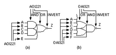
The AND-OR-INVERT (AOI) and the OR-AND-INVERT (OAI) logic cells are particularly efficient in CMOS. Figure 2.12 shows an AOI221 and an OAI321 logic cell (the logic symbols in Figure 2.12 are not standards, but are widely used). All indices (the indices are the numbers after AOI or OAI) in the logic cell name greater than 1 correspond to the inputs to the first level or stage the AND gate(s) in an AOI cell, for example. An index of '1' corresponds to a direct input to the second-stage cell. We write indices in descending order; so it is AOI221 and not AOI122 (but both are equivalent cells), and AOI32 not AOI23. If we have more than one direct input to the second stage we repeat the '1'; thus an AOI211 cell performs the function Z = (A.B + C + D)'. A three-input NAND cell is an OAI111, but calling it that would be very confusing. These rules are not standard, but form a convention that we shall adopt and one that is widely used in the ASIC industry.
There are many ways to represent the logical operator, AND. I shall use the middle dot and write A · B (rather than AB, A.B, or A ' B); occasionally I may use AND(A, B). Similarly I shall write A + B as well as OR(A, B). I shall use an apostrophe like this, A', to denote the complement of A rather than A since sometimes it is difficult or inappropriate to use an overbar ( vinculum ) or diacritical mark (macron). It is possible to misinterpret AB' as A B rather than AB (but the former alternative would be A · B' in my convention). I shall be careful in these situations.
FIGURE 2.12 Naming and numbering complex CMOS combinational cells. (a) An AND-OR-INVERT cell, an AOI221. (b) An OR-AND-INVERT cell, an OAI321. Numbering is always in descending order.
We can express the function of the AOI221 cell in Figure 2.12(a) as
Z = (A · B + C · D + E)' . (2.25)
We can also write this equation unambiguously as Z = OAI221(A, B, C, D, E), just as we might write X = NAND (I, J, K) to describe the logic function
X = (I · J · K)'.
This notation is useful because, for example, if we write OAI321(P, Q, R, S, T, U) we immediately know that U (the sixth input) is the (only) direct input connected to the second stage. Sometimes we need to refer to particular inputs without listing them all. We can adopt another convention that letters of the input names change with the index position. Now we can refer to input B2 of an AOI321 cell, for example, and know which input we are talking about without writing
Z = AOI321(A1, A2, A3, B1, B2, C) . (2.26)
Table 2.10 shows the AOI family of logic cells with three indices (with branches in the family for AOI, OAI, AO, and OA cells). There are 5 types and 14 separate members of each branch of this family. There are thus 4 ¥ 14 = 56 cells of the type X abc where X = {OAI, AOI, OA, AO} and each of the indexes a , b , and c can range from 1 to 3. We form the AND-OR (AO) and OR-AND (OA) cells by adding an inverter to the output of an AOI or OAI cell.
TABLE 2.10 The AOI family of cells with three index numbers or less.
Cell type 1 |
Cells |
Number of unique cells |
||
Xa1 |
|
|
X21, X31 |
2 |
Xa11 |
X211, X311 |
2 |
||
Xab |
X22, X33, X32 |
3 |
||
Xab1 |
X221, X331, X321 |
3 |
||
Xabc |
X222, X333, X332, X322 |
4 |
||
Total |
|
14 |
||
2.4.1 Pushing Bubbles
The AOI and OAI logic cells can be built using a single stage in CMOS using series parallel networks of transistors called stacks. Figure 2.13 illustrates the procedure to build the n -channel and p -channel stacks, using the AOI221 cell as an example.
FIGURE 2.13 Constructing a CMOS logic cell an AOI221. (a) First build the dual icon by using de Morgan s theorem to push inversion bubbles to the inputs. (b) Next build the n -channel and p -channel stacks from series and parallel combinations of transistors. (c) Adjust transistor sizes so that the n- channel and p -channel stacks have equal strengths.
Here are the steps to construct any single-stage combinational CMOS logic cell:
1.Draw a schematic icon with an inversion (bubble) on the last cell (the bubble-out schematic). Use de Morgan s theorems A NAND is an OR with inverted inputs and a NOR is an AND with inverted inputs to push the output bubble back to the inputs (this the dual icon or bubble-in schematic).
2.Form the n -channel stack working from the inputs on the bubble-out schematic: OR translates to a parallel connection, AND translates to a series connection. If you have a bubble at an input, you need an inverter.
3.Form the p -channel stack using the bubble-in schematic (ignore the inversions at the inputs the bubbles on the gate terminals of the p -channel transistors take care of these). If you do not have a bubble at the input gate terminals, you need an inverter (these will be the same input gate terminals that had bubbles in the bubble-out schematic).
The two stacks are network duals (they can be derived from each other by swapping series connections for parallel, and parallel for series connections). The n -channel stack implements the strong '0's of the function and the p -channel stack provides the strong '1's. The final step is to adjust the drive strength of the logic cell by sizing the transistors.
2.4.2 Drive Strength
Normally we ratio the sizes of the n -channel and p -channel transistors in an inverter so that both types of transistors have the same resistance, or drive strength . That is, we make b n = b p . At low dopant concentrations and low
electric fields m n is about twice m p . To compensate we make the shape factor, W/L, of the p -channel transistor in an inverter about twice that of the n -channel transistor (we say the logic has a ratio of 2). Since the transistor lengths are normally equal to the minimum poly width for both types of transistors, the ratio of the transistor widths is also equal to 2. With the high dopant concentrations and high electric fields in submicron transistors the difference in mobilities is lesstypically between 1 and 1.5.
Logic cells in a library have a range of drive strengths. We normally call the minimum-size inverter a 1X inverter. The drive strength of a logic cell is often used as a suffix; thus a 1X inverter has a cell name such as INVX1 or INVD1. An inverter with transistors that are twice the size will be an INVX2. Drive strengths are normally scaled in a geometric ratio, so we have 1X, 2X, 4X, and (sometimes) 8X or even higher, drive-strength cells. We can size a logic cell using these basic rules:
●Any string of transistors connected between a power supply and the output in a cell with 1X drive should have the same resistance as the n -channel transistor in a 1X inverter.
●A transistor with shape factor W 1 /L 1 has a resistance proportional to L 1 /W 1 (so the larger W 1 is, the smaller the resistance).
●Two transistors in parallel with shape factors W 1 /L 1 and W 2 /L 2 are equivalent to a single transistor (W 1 /L 1 + W 2 /L 2 )/1. For example, a 2/1 in parallel with a 3/1 is a 5/1.
●Two transistors, with shape factors W 1 /L 2 and W 2 /L 2 , in series are equivalent to a single 1/(L 1 /W 1 + L 2 /W 2 ) transistor.
For example, a transistor with shape factor 3/1 (we shall call this a 3/1 ) in series with another 3/1 is equivalent to a 1/((1/3) + (1/3)) or a 3/2. We can use the following method to calculate equivalent transistor sizes:
●To add transistors in parallel, make all the lengths 1 and add the widths.
●To add transistors in series, make all the widths 1 and add the lengths.
We have to be careful to keep W and L reasonable. For example, a 3/1 in series with a 2/1 is equivalent to a 1/((1/3) + (1/2)) or 1/0.83. Since we cannot make a device 2 l wide and 1.66 l long, a 1/0.83 is more naturally written as 3/2.5. We like to keep both W and L as integer multiples of 0.5 (equivalent to making W and L integer multiples of l ), but W and L must be greater than 1.
In Figure 2.13(c) the transistors in the AOI221 cell are sized so that any string through the p -channel stack has a drive strength equivalent to a 2/1 p -channel transistor (we choose the worst case, if more than one transistor in parallel is conducting then the drive strength will be higher). The n -channel stack is sized so that it has a drive strength of a 1/1 n -channel transistor. The ratio in this library is thus 2.
If we were to use four drive strengths for each of the AOI family of cells shown in Table 2.10, we would have a total of 224 combinational library cells just for the AOI family. The synthesis tools can handle this number of cells, but we may not be able to design this many cells in a reasonable amount of time. Section 3.3,Logical Effort, will help us choose the most logically efficient cells.
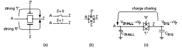
2.4.3 Transmission Gates
Figure 2.14(a) and (b) shows a CMOS transmission gate ( TG , TX gate, pass gate, coupler). We connect a p -channel transistor (to transmit a strong '1') in parallel with an n -channel transistor (to transmit a strong '0').
FIGURE 2.14 CMOS transmission gate (TG). (a) An n- channel and p -channel transistor in parallel form a TG. (b) A common symbol for a TG. (c) The charge-sharing problem.
We can express the function of a TG as
Z = TG(A, S) , (2.27)
but this is ambiguous if we write TG(X, Y), how do we know if X is connected to the gates or sources/drains of the TG? We shall always define TG(X, Y) when we use it. It is tempting to write TG(A, S) = A · S, but what is the value of Z when S ='0' in Figure 2.14(a), since Z is then left floating? A TG is a switch, not an AND logic cell.
There is a potential problem if we use a TG as a switch connecting a node Z that has a large capacitance, C BIG , to an input node A that has only a small
capacitance C SMALL (see Figure 2.14c). If the initial voltage at A is V SMALL and the initial voltage at Z is V BIG , when we close the TG (by setting S = '1') the final voltage on both nodes A and Z is
C BIG V BIG + C SMALL V SMALL
V F = |
. (2.28) |
C BIG + C SMALL |
|
Imagine we want to drive a '0' onto node Z from node A. Suppose C BIG = 0.2 pF
(about 10 standard loads in a 0.5 m m process) and C SMALL = 0.02 pF, V BIG = 0 V and V SMALL = 5 V; then

(0.2 ¥ 10 12 ) (0) + (0.02 ¥ 10 12 ) (5)
V F = |
= 0.45 V . (2.29) |
(0.2 ¥ 10 12 ) + (0.02 ¥ 10 12 ) |
|
This is not what we want at all, the big capacitor has forced node A to a voltage close to a '0'. This type of problem is known as charge sharing . We should make sure that either (1) node A is strong enough to overcome the big capacitor, or (2) insulate node A from node Z by including a buffer (an inverter, for example) between node A and node Z. We must not use charge to drive another logic cellonly a logic cell can drive a logic cell.
If we omit one of the transistors in a TG (usually the p -channel transistor) we have a pass transistor . There is a branch of full-custom VLSI design that uses pass-transistor logic. Much of this is based on relay-based logic, since a single transistor switch looks like a relay contact. There are many problems associated with pass-transistor logic related to charge sharing, reduced noise margins, and the difficulty of predicting delays. Though pass transistors may appear in an ASIC cell inside a library, they are not used by ASIC designers.
FIGURE 2.15 The CMOS multiplexer (MUX). (a) A noninverting 2:1 MUX using transmission gates without buffering. (b) A symbol for a MUX (note how the inputs are labeled). (c) An IEEE standard symbol for a MUX. (d) A nonstandard, but very common, IEEE symbol for a MUX. (e) An inverting MUX with output buffer. (f) A noninverting buffered MUX.
We can use two TGs to form a multiplexer (or multiplexor people use both orthographies) as shown in Figure 2.15(a). We often shorten multiplexer to MUX
. The MUX function for two data inputs, A and B, with a select signal S, is
Z = TG(A, S') + TG(B, S) . (2.30)
We can write this as Z = A · S' + B · S, since node Z is always connected to one or other of the inputs (and we assume both are driven). This is a two-input MUX (2-to-1 MUX or 2:1 MUX). Unfortunately, we can also write the MUX function as Z = A · S + B · S', so it is difficult to write the MUX function unambiguously as Z = MUX(X, Y, Z). For example, is the select input X, Y, or Z? We shall define the function MUX(X, Y, Z) each time we use it. We must also be careful to label a MUX if we use the symbol shown in Figure 2.15(b). Symbols for a

MUX are shown in Figure 2.15(b d). In the IEEE notation 'G' specifies an AND dependency. Thus, in Figure 2.15(c), G = '1' selects the input labeled '1'.
Figure 2.15(d) uses the common control block symbol (the notched rectangle). Here, G1 = '1' selects the input '1', and G1 = '0' selects the input ' 1 '. Strictly this form of IEEE symbol should be used only for elements with more than one section controlled by common signals, but the symbol of Figure 2.15(d) is used often for a 2:1 MUX.
The MUX shown in Figure 2.15(a) works, but there is a potential charge-sharing problem if we cascade MUXes (connect them in series). Instead most ASIC libraries use MUX cells built with a more conservative approach. We could buffer the output using an inverter (Figure 2.15e), but then the MUX becomes inverting. To build a safe, noninverting MUX we can buffer the inputs and output (Figure 2.15f) requiring 12 transistors, or 3 gate equivalents (only the gate equivalent counts are shown from now on).
Figure 2.16 shows how to use an OAI22 logic cell (and an inverter) to implement an inverting MUX. The implementation in equation form (2.5 gates) is
ZN = A' · S' + B' · S
=[(A' · S')' · (B' · S)']'
=[ (A + S) · (B + S')]'
=OAI22[A, S, B, NOT(S)] . (2.31)
(both A' and NOT(A) represent an inverter, depending on which representation is most convenient they are equivalent). I often use an equation to describe a cell implementation.
FIGURE 2.16 An inverting 2:1 MUX based on an
OAI22 cell.
The following factors will determine which MUX implementation is best:
1.Do we want to minimize the delay between the select input and the output or between the data inputs and the output?
2.Do we want an inverting or noninverting MUX?
3.Do we object to having any logic cell inputs tied directly to the source/drain diffusions of a transmission gate? (Some companies forbid such transmission-gate inputs since some simulation tools cannot handle them.)
4.Do we object to any logic cell outputs being tied to the source/drain of a

transmission gate? (Some companies will not allow this because of the dangers of charge sharing.)
5. What drive strength do we require (and is size or speed more important)?
A minimum-size TG is a little slower than a minimum-size inverter, so there is not much difference between the implementations shown in Figure 2.15 and Figure 2.16, but the difference can become important for 4:1 and larger MUXes.
2.4.4 Exclusive-OR Cell
The two-input exclusive-OR ( XOR , EXOR, not-equivalence, ring-OR) function is
A1 • A2 = XOR(A1, A2) = A1 · A2' + A1' · A2 . (2.32)
We are now using multiletter symbols, but there should be no doubt that A1' means anything other than NOT(A1). We can implement a two-input XOR using a MUX and an inverter as follows (2 gates):
XOR(A1, A2) = MUX[NOT(A1), A1, A2] , (2.33)
where
MUX(A, B, S) = A · S + B · S ' . (2.34)
This implementation only buffers one input and does not buffer the MUX output. We can use inverter buffers (3.5 gates total) or an inverting MUX so that the XOR cell does not have any external connections to source/drain diffusions as follows (3 gates total):
XOR(A1, A2) = NOT[MUX(NOT[NOT(A1)], NOT(A1), A2)] . (2.35)
We can also implement a two-input XOR using an AOI21 (and a NOR cell), since
XOR(A1, A2) = A1 · A2' + A1' · A2
=[ (A1 ·A2) + (A1 + A2)' ]'
=AOI21[A1, A2, NOR(A1, A2)], (2.36)
(2.5 gates). Similarly we can implement an exclusive-NOR (XNOR, equivalence) logic cell using an inverting MUX (and two inverters, total 3.5 gates) or an OAI21 logic cell (and a NAND cell, total 2.5 gates) as follows (using the MUX function of Eq. 2.34):
XNOR(A1, A2) = A1 · A2 + NOT(A1) · NOT(A2
= NOT[NOT[MUX(A1, NOT (A1), A2]]
= OAI21[A1, A2, NAND(A1, A2)] . |
(2.37) |
1. Xabc: X = {AOI, AO, OAI, OA}; a, b, c = {2, 3}; { } means choose one.
2.5 Sequential Logic Cells
There are two main approaches to clocking in VLSI design: multiphase clocks or a single clock and synchronous design . The second approach has the following key advantages: (1) it allows automated design, (2) it is safe, and (3) it permits vendor signoff (a guarantee that the ASIC will work as simulated). These advantages of synchronous design (especially the last one) usually outweigh every other consideration in the choice of a clocking scheme. The vast majority of ASICs use a rigid synchronous design style.
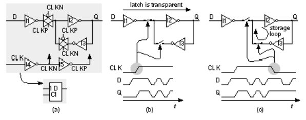
2.5.1 Latch
Figure 2.17(a) shows a sequential logic cell a latch . The internal clock signals, CLKN (N for negative) and CLKP (P for positive), are generated from the system clock, CLK, by two inverters (I4 and I5) that are part of every latch cell it is usually too dangerous to have these signals supplied externally, even though it would save space.
FIGURE 2.17 CMOS latch. (a) A positive-enable latch using transmission gates without output buffering, the enable (clock) signal is buffered inside the latch.
(b) A positive-enable latch is transparent while the enable is high. (c) The latch stores the last value at D when the enable goes low.
To emphasize the difference between a latch and flip-flop, sometimes people refer to the clock input of a latch as an enable . This makes sense when we look at Figure 2.17(b), which shows the operation of a latch. When the clock input is high, the latch is transparent changes at the D input appear at the output Q (quite different from a flip-flop as we shall see). When the enable (clock) goes low (Figure 2.17c), inverters I2 and I3 are connected together, forming a storage loop
that holds the last value on D until the enable goes high again. The storage loop will hold its state as long as power is on; we call this a static latch. A sequential logic cell is different from a combinational cell because it has this feature of storage or memory.
Notice that the output Q is unbuffered and connected directly to the output of I2 (and the input of I3), which is a storage node. In an ASIC library we are conservative and add an inverter to buffer the output, isolate the sensitive storage node, and thus invert the sense of Q. If we want both Q and QN we have to add two inverters to the circuit of Figure 2.17(a). This means that a latch requires seven inverters and two TGs (4.5 gates).
The latch of Figure 2.17(a) is a positive-enable D latch, active-high D latch, or transparent-high D latch (sometimes people also call this a D-type latch). A negative-enable (active-low) D latch can be built by inverting all the clock polarities in Figure 2.17(a) (swap CLKN for CLKP and vice-versa).
2.5.2 Flip-Flop
Figure 2.18(a) shows a flip-flop constructed from two D latches: a master latch (the first one) and a slave latch . This flip-flop contains a total of nine inverters and four TGs, or 6.5 gates. In this flip-flop design the storage node S is buffered and the clock-to-Q delay will be one inverter delay less than the clock-to-QN delay.
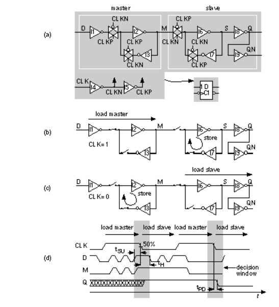
FIGURE 2.18 CMOS flip-flop. (a) This negative-edge triggered flip-flop consists of two latches: master and slave. (b) While the clock is high, the master latch is loaded. (c) As the clock goes low, the slave latch loads the value of the master latch. (d) Waveforms illustrating the definition of the flip-flop setup time t SU , hold time t H , and propagation delay from clock to Q, t PD .
In Figure 2.18(b) the clock input is high, the master latch is transparent, and node M (for master) will follow the D input. Meanwhile the slave latch is disconnected from the master latch and is storing whatever the previous value of Q was. As the clock goes low (the negative edge) the slave latch is enabled and will update its state (and the output Q) to the value of node M at the negative edge of the clock. The slave latch will then keep this value of M at the output Q, despite any changes at the D input while the clock is low (Figure 2.18c). When the clock goes high again, the slave latch will store the captured value of M (and we are back where we started our explanation).
The combination of the master and slave latches acts to capture or sample the D input at the negative clock edge, the active clock edge . This type of flip-flop is a
negative-edge triggered flip-flop and its behavior is quite different from a latch. The behavior is shown on the IEEE symbol by using a triangular notch to denote an edge-sensitive input. A bubble shows the input is sensitive to the negative edge. To build a positive-edge triggered flip-flop we invert the polarity of all the clocks as we did for a latch.
The waveforms in Figure 2.18(d) show the operation of the flip-flop as we have described it, and illustrate the definition of setup time ( t SU ), hold time ( t H ), and clock-to-Q propagation delay ( t PD ). We must keep the data stable (a fixed logic '1' or '0') for a time t SU prior to the active clock edge, and stable for a time t H after the active clock edge (during the decision window shown).
In Figure 2.18(d) times are measured from the points at which the waveforms cross 50 percent of V DD . We say the trip point is 50 percent or 0.5. Common choices are 0.5 or 0.65/0.35 (a signal has to reach 0.65 V DD to be a '1', and reach 0.35 V DD to be a '0'), or 0.1/0.9 (there is no standard way to write a trip point). Some vendors use different trip points for the input and output waveforms (especially in I/O cells).
The flip-flop in Figure 2.18(a) is a D flip-flop and is by far the most widely used type of flip-flop in ASIC design. There are other types of flip-flops J-K, T (toggle), and S-R flip-flops that are provided in some ASIC cell libraries mainly for compatibility with TTL design. Some people use the term register to mean an array (more than one) of flip-flops or latches (on a data bus, for example), but some people use register to mean a single flip-flop or a latch. This is confusing since flip-flops and latches are quite different in their behavior. When I am talking about logic cells, I use the term register to mean more than one flip-flop.
To add an asynchronous set (Q to '1') or asynchronous reset (Q to '0') to the flip-flop of Figure 2.18(a), we replace one inverter in both the master and slave latches with two-input NAND cells. Thus, for an active-low set, we replace I2 and I7 with two-input NAND cells, and, for an active-low reset, we replace I3 and I6. For both set and reset we replace all four inverters: I2, I3, I6, and I7. Some TTL flip-flops have dominant reset or dominant set , but this is difficult (and dangerous) to do in ASIC design. An input that forces Q to '1' is sometimes also called preset . The IEEE logic symbols use 'P' to denote an input with a presetting action. An input that forces Q to '0' is often also called clear . The IEEE symbols use 'R' to denote an input with a resetting action.
2.5.3 Clocked Inverter
Figure 2.19 shows how we can derive the structure of a clocked inverter from the series combination of an inverter and a TG. The arrows in Figure 2.19(b) represent the flow of current when the inverter is charging ( I R ) or discharging ( I F ) a load capacitance through the TG. We can break the connection between the inverter cells and use the circuit of Figure 2.19(c) without substantially affecting
the operation of the circuit. The symbol for the clocked inverter shown in Figure 2.19(d) is common, but by no means a standard.
FIGURE 2.19 Clocked inverter. (a) An inverter plus transmission gate (TG).
(b) The current flow in the inverter and TG allows us to break the connection between the transistors in the inverter. (c) Breaking the connection forms a clocked inverter. (d) A common symbol.
We can use the clocked inverter to replace the inverter TG pairs in latches and flip-flops. For example, we can replace one or both of the inverters I1 and I3 (together with the TGs that follow them) in Figure 2.17(a) by clocked inverters. There is not much to choose between the different implementations in this case, except that layout may be easier for the clocked inverter versions (since there is one less connection to make).
More interesting is the flip-flop design: We can only replace inverters I1, I3, and I7 (and the TGs that follow them) in Figure 2.18(a) by clocked inverters. We cannot replace inverter I6 because it is not directly connected to a TG. We can replace the TG attached to node M with a clocked inverter, and this will invert the sense of the output Q, which thus becomes QN. Now the clock-to-Q delay will be slower than clock-to-QN, since Q (which was QN) now comes one inverter later than QN.
If we wish to build a flip-flop with a fast clock-to-QN delay it may be better to build it using clocked inverters and use inverters with TGs for a flip-flop with a fast clock-to-Q delay. In fact, since we do not always use both Q and QN outputs of a flip-flop, some libraries include Q only or QN only flip-flops that are slightly smaller than those with both polarity outputs. It is slightly easier to layout clocked inverters than an inverter plus a TG, so flip-flops in commercial libraries include a mixture of clocked-inverter and TG implementations.
2.6 Datapath Logic Cells
Suppose we wish to build an n -bit adder (that adds two n -bit numbers) and to exploit the regularity of this function in the layout. We can do so using a datapath structure.
The following two functions, SUM and COUT, implement the sum and carry out for a full adder ( FA ) with two data inputs (A, B) and a carry in, CIN:
SUM = A • B • CIN = SUM(A, B, CIN) = PARITY(A, B, CIN) , (2.38)
COUT = A · B + A · CIN + B · CIN = MAJ(A, B, CIN). |
(2.39) |
The sum uses the parity function ('1' if there are an odd numbers of '1's in the inputs). The carry out, COUT, uses the 2-of-3 majority function ('1' if the majority of the inputs are '1'). We can combine these two functions in a single FA logic cell, ADD(A[ i ], B[ i ], CIN, S[ i ], COUT), shown in Figure 2.20(a), where
S[ i ] = SUM (A[ i ], B[ i ], CIN) , (2.40)
COUT = MAJ (A[ i ], B[ i ], CIN) . (2.41)
Now we can build a 4-bit ripple-carry adder ( RCA ) by connecting four of these ADD cells together as shown in Figure 2.20(b). The i th ADD cell is arranged with the following: two bus inputs A[ i ], B[ i ]; one bus output S[ i ]; an input, CIN, that is the carry in from stage ( i 1) below and is also passed up to the cell above as an output; and an output, COUT, that is the carry out to stage ( i + 1) above. In the 4-bit adder shown in Figure 2.20(b) we connect the carry input, CIN[0], to VSS and use COUT[3] and COUT[2] to indicate arithmetic overflow (in Section 2.6.1 we shall see why we may need both signals). Notice that we build the ADD cell so that COUT[2] is available at the top of the datapath when we need it.
Figure 2.20(c) shows a layout of the ADD cell. The A inputs, B inputs, and S outputs all use m1 interconnect running in the horizontal direction we call these data signals. Other signals can enter or exit from the top or bottom and run vertically across the datapath in m2 we call these control signals. We can also use m1 for control and m2 for data, but we normally do not mix these approaches in the same structure. Control signals are typically clocks and other signals common to elements. For example, in Figure 2.20(c) the carry signals, CIN and COUT, run vertically in m2 between cells. To build a 4-bit adder we stack four ADD cells creating the array structure shown in Figure 2.20(d). In this case the A and B data bus inputs enter from the left and bus S, the sum, exits at the right, but we can connect A, B, and S to either side if we want.
The layout of buswide logic that operates on data signals in this fashion is called a datapath . The module ADD is a datapath cell or datapath element . Just as we do for standard cells we make all the datapath cells in a library the same height so we can abut
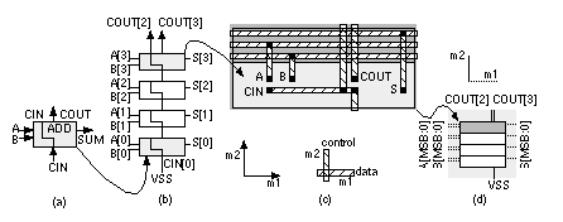
other datapath cells on either side of the adder to create a more complex datapath. When people talk about a datapath they always assume that it is oriented so that increasing the size in bits makes the datapath grow in height, upwards in the vertical direction, and adding different datapath elements to increase the function makes the datapath grow in width, in the horizontal direction but we can rotate and position a completed datapath in any direction we want on a chip.
FIGURE 2.20 A datapath adder. (a) A full-adder (FA) cell with inputs (A and B), a carry in, CIN, sum output, S, and carry out, COUT. (b) A 4-bit adder. (c) The layout, using two-level metal, with data in m1 and control in m2. In this example the wiring is completed outside the cell; it is also possible to design the datapath cells to contain the wiring. Using three levels of metal, it is possible to wire over the top of the datapath cells. (d) The datapath layout.
What is the difference between using a datapath, standard cells, or gate arrays? Cells are placed together in rows on a CBIC or an MGA, but there is no generally no regularity to the arrangement of the cells within the rows we let software arrange the cells and complete the interconnect. Datapath layout automatically takes care of most of the interconnect between the cells with the following advantages:
●Regular layout produces predictable and equal delay for each bit.
●Interconnect between cells can be built into each cell.
There are some disadvantages of using a datapath:
●The overhead (buffering and routing the control signals, for example) can make a narrow (small number of bits) datapath larger and slower than a standard-cell (or even gate-array) implementation.
●Datapath cells have to be predesigned (otherwise we are using full-custom design) for use in a wide range of datapath sizes. Datapath cell design can be harder than designing gate-array macros or standard cells.
●Software to assemble a datapath is more complex and not as widely used as software for assembling standard cells or gate arrays.
There are some newer standard-cell and gate-array tools that can take advantage of regularity in a design and position cells carefully. The problem is in finding the regularity if it is not specified. Using a datapath is one way to specify regularity to ASIC design tools.
2.6.1 Datapath Elements
Figure 2.21 shows some typical datapath symbols for an adder (people rarely use the IEEE standards in ASIC datapath libraries). I use heavy lines (they are 1.5 point wide) with a stroke to denote a data bus (that flows in the horizontal direction in a datapath), and regular lines (0.5 point) to denote the control signals (that flow vertically in a datapath). At the risk of adding confusion where there is none, this stroke to indicate a data bus has nothing to do with mixed-logic conventions. For a bus, A[31:0] denotes a 32-bit bus with A[31] as the leftmost or most-significant bit or MSB , and A[0] as the least-significant bit or LSB . Sometimes we shall use A[MSB] or A[LSB] to refer to these bits. Notice that if we have an n -bit bus and LSB = 0, then MSB = n 1. Also, for example, A[4] is the fifth bit on the bus (from the LSB). We use a ' S ' or 'ADD' inside the symbol to denote an adder instead of '+', so we can attach ' ' or '+/ ' to the inputs for a subtracter or adder/subtracter.
FIGURE 2.21 Symbols for a datapath adder. (a) A data bus is shown by a heavy line (1.5 point) and a bus symbol. If the bus is n -bits wide then MSB = n 1. (b) An alternative symbol for an adder. (c) Control signals are shown as lightweight (0.5 point) lines.
Some schematic datapath symbols include only data signals and omit the control signals but we must not forget them. In Figure 2.21, for example, we may need to explicitly tie CIN[0] to VSS and use COUT[MSB] and COUT[MSB 1] to detect overflow. Why might we need both of these control signals? Table 2.11 shows the process of simple arithmetic for the different binary number representations, including unsigned, signed magnitude, ones complement, and two s complement.
TABLE 2.11 Binary arithmetic.
Binary Number Representation
Operation
|
Unsigned |
|
no change |
3 = |
0011 |
3 = |
NA |
zero = |
0000 |
Signed |
Ones |
Two s |
magnitude |
complement |
complement |
if positive |
if negative then flip |
if negative then {flip |
then MSB = 0 |
||
else MSB = 1 |
bits |
bits; add 1} |
|
|
|
0011 |
0011 |
0011 |
1011 |
1100 |
1101 |
0000 or 1000 |
1111 or 0000 |
0000 |
max. |
1111 = 15 |
|
positive = |
||
|
||
max. |
0000= 0 |
|
negative = |
||
addition = |
|
|
S = A + B |
|
|
= addend + |
|
|
augend |
S = A + B |
SG(A) = sign of A
0111 = 7
1111 = 7
if SG(A) = SG(B) then S = A + B
else { if B < A then S = A B
else S = B A}
0111 = 7
1000 = 7
S =
A + B +
COUT[MSB]
COUT is carry out
addition result:
OR =
COUT[MSB]
OV = overflow,
OR = out
COUT is
of range
carry out
SG(S) = sign of S
NA
S = A + B
subtraction
=
if SG(A) =
SG(B) then
OV =
OV =
COUT[MSB] XOR(COUT[MSB],
COUT[MSB 1])
else OV = 0 (impossible)
if SG(A) = SG(B) then SG(S) = SG(A)
else { if B < A NA then SG(S) = SG(A)
else SG(S) = SG(B)}
D = A B |
|
SG(B) = |
Z = B (negate); |
|
D = A B |
NOT(SG(B)); |
|||
= minuend |
|
D = A + Z |
||
|
D = A + B |
|||
|
|
|
||
|
|
|
|
|
subtrahend |
|
|
|
|
subtraction |
|
|
|
|
result : |
OR = |
|
|
|
|
|
|
||
OV = |
BOUT[MSB] |
as in addition |
as in addition |
|
|
||||
overflow, |
BOUT is |
|||
|
|
|||
|
|
|
||
OR = out |
borrow out |
|
|
|
|
|
|
||
of range |
|
|
|
0111 = 7
1000 = 8
S = A + B
OV =
XOR(COUT[MSB], COUT[MSB 1])
NA
Z = B (negate);
D = A + Z
as in addition
negation : |
|
Z = A; |
|
|
Z = A |
NA |
SG(Z) = |
Z = NOT(A) |
Z = NOT(A) + 1 |
|
|
|
||
(negate) |
|
NOT(SG(A)) |
|
|
2.6.2 Adders
We can view addition in terms of generate , G[ i ], and propagate , P[ i ], signals.
method 1 |
method 2 |
|
G[i] = A[i] · B[i] |
G[ i ] = A[ i ] · B[ i ] |
(2.42) |
P[ i ] = A[ i ] • B[ i |
P[ i ] = A[ i ] + B[ i ] |
(2.43) |
C[ i ] = G[ i ] + P[ i ] · C[ i 1]C[ i ] = G[ i ] + P[ i ] · C[ i 1](2.44)
S[ i ] = P[ i ] • C[ i 1] |
S[ i ] = A[ i ] • B[ i ] • C[ i 1] (2.45) |
where C[ i ] is the carry-out signal from stage i , equal to the carry in of stage ( i + 1). Thus, C[ i ] = COUT[ i ] = CIN[ i + 1]. We need to be careful because C[0] might represent either the carry in or the carry out of the LSB stage. For an adder we set the carry in to the first stage (stage zero), C[ 1] or CIN[0], to '0'. Some people use delete
(D) or kill (K) in various ways for the complements of G[i] and P[i], but unfortunately others use C for COUT and D for CIN so I avoid using any of these. Do not confuse the two different methods (both of which are used) in Eqs. 2.42 2.45 when forming the sum, since the propagate signal, P[ i ] , is different for each method.
Figure 2.22(a) shows a conventional RCA. The delay of an n -bit RCA is proportional to n and is limited by the propagation of the carry signal through all of the stages. We can reduce delay by using pairs of go-faster bubbles to change AND and OR gates to fast two-input NAND gates as shown in Figure 2.22(a). Alternatively, we can write the equations for the carry signal in two different ways:
either C[ i ] = A[ i ] · B[ i ] + P[ i ] · C[ i 1] |
(2.46) |
|
or |
C[ i ] = (A[ i ] + B[ i ] ) · (P[ i ]' + C[ i 1]),(2.47) |
|
where P[ i ]'= NOT(P[ i ]). Equations 2.46 and 2.47 allow us to build the carry chain from two-input NAND gates, one per cell, using different logic in even and odd stages (Figure 2.22b):
even stages |
odd stages |
C1[i]' = P[i ] · C3[i 1] · C4[i 1]C3[i]' = P[i ] · C1[i 1] · C2[i 1](2.48)
C2[i] = A[i ] + B[i ] |
C4[i]' = A[i ] · B[i ] |
(2.49) |
C[i] = C1[i ] · C2[i ] |
C[i] = C3[i ] ' + C4[i ]' |
(2.50) |
(the carry inputs to stage zero are C3[ 1] = C4[ 1] = '0'). We can use the RCA of Figure 2.22(b) in a datapath, with standard cells, or on a gate array.
Instead of propagating the carries through each stage of an RCA, Figure 2.23 shows a different approach. A carry-save adder ( CSA ) cell CSA(A1[ i ], A2[ i ], A3[ i ], CIN, S1[ i ], S2[ i ], COUT) has three outputs:
S1[ i ] = CIN , |
(2.51) |
S2[ i ] = A1[ i ] • A2[ i ] • A3[ i ] = PARITY(A1[ i ], A2[ i ], A3[ i ]) , |
(2.52) |
COUT = A1[ i ] · A2[ i ] + [(A1[ i ] + A2[ i ]) · A3[ i ]] = MAJ(A1[ i ], A2[ i ],
(2.53)
A3[ i ]) .
The inputs, A1, A2, and A3; and outputs, S1 and S2, are buses. The input, CIN, is the carry from stage ( i 1). The carry in, CIN, is connected directly to the output bus S1indicated by the schematic symbol (Figure 2.23a). We connect CIN[0] to VSS. The output, COUT, is the carry out to stage ( i + 1).
A 4-bit CSA is shown in Figure 2.23(b). The arithmetic overflow signal for ones complement or two s complement arithmetic, OV, is XOR(COUT[MSB], COUT[MSB1]) as shown in Figure 2.23(c). In a CSA the carries are saved at each stage and shifted left onto the bus S1. There is thus no carry propagation and the delay of a CSA is constant. At the output of a CSA we still need to add the S1 bus (all the saved carries) and the S2 bus (all the sums) to get an n -bit result using a final stage that is not shown in Figure 2.23(c). We might regard the n -bit sum as being encoded in the two buses, S1 and S2, in the form of the parity and majority functions.
We can use a CSA to add multiple inputs as an example, an adder with four 4-bit inputs is shown in Figure 2.23(d). The last stage sums two input buses using a carry-propagate adder ( CPA ). We have used an RCA as the CPA in Figure 2.23(d) and (e), but we can use any type of adder. Notice in Figure 2.23(e) how the two CSA cells and the RCA cell abut together horizontally to form a bit slice (or slice) and then the slices are stacked vertically to form the datapath.
FIGURE 2.22 The carry-save adder (CSA). (a) A CSA cell. (b) A 4-bit CSA.
(c) Symbol for a CSA. (d) A four-input CSA. (e) The datapath for a four-input, 4-bit adder using CSAs with a ripple-carry adder (RCA) as the final stage. (f) A pipelined adder. (g) The datapath for the pipelined version showing the pipeline registers as well as the clock control lines that use m2.
We can register the CSA stages by adding vectors of flip-flops as shown in
Figure 2.23(f). This reduces the adder delay to that of the slowest adder stage, usually the CPA. By using registers between stages of combinational logic we use pipelining to increase the speed and pay a price of increased area (for the registers) and introduce latency . It takes a few clock cycles (the latency, equal to n clock cycles for an n -stage pipeline) to fill the pipeline, but once it is filled, the answers emerge every clock cycle. Ferris wheels work much the same way. When the fair opens it takes a while (latency) to fill the wheel, but once it is full the people can get on and off every few seconds. (We can also pipeline the RCA of Figure 2.20. We add i registers on the A and B inputs before ADD[ i ] and add ( n i ) registers after the output S[ i ], with a single register before each C[ i ].)
The problem with an RCA is that every stage has to wait to make its carry decision, C[ i ], until the previous stage has calculated C[ i 1]. If we examine the propagate signals we can bypass this critical path. Thus, for example, to bypass the carries for bits 4 7 (stages 5 8) of an adder we can compute BYPASS = P[4].P[5].P[6].P[7] and then use a MUX as follows:
C[7] = (G[7] + P[7] · C[6]) · BYPASS' + C[3] · BYPASS . (2.54)
Adders based on this principle are called carry-bypass adders ( CBA ) [Sato et al., 1992]. Large, custom adders employ Manchester-carry chains to compute the carries and the bypass operation using TGs or just pass transistors [Weste and Eshraghian, 1993, pp. 530 531]. These types of carry chains may be part of a predesigned ASIC adder cell, but are not used by ASIC designers.
Instead of checking the propagate signals we can check the inputs. For example we can compute SKIP = (A[ i 1] • B[ i 1]) + (A[ i ] • B[ i ] ) and then use a 2:1 MUX to select C[ i ]. Thus,
CSKIP[ i ] = (G[ i ] + P[ i ] · C[ i 1]) · SKIP' + C[ i 2] · SKIP .(2.55)
This is a carry-skip adder [Keutzer, Malik, and Saldanha, 1991; Lehman, 1961]. Carry-bypass and carry-skip adders may include redundant logic (since the carry is computed in two different ways we just take the first signal to arrive). We must be careful that the redundant logic is not optimized away during logic synthesis.
If we evaluate Eq. 2.44 recursively for i = 1, we get the following:
C[1] = G[1] + P[1] · C[0]
= G[1] + P[1] · (G[0] + P[1] · C[ 1])
= G[1] + P[1] · G[0] . |
(2.56) |
This result means that we can look ahead by two stages and calculate the carry into the third stage (bit 2), which is C[1], using only the first-stage inputs (to calculate G[0]) and the second-stage inputs. This is a carry-lookahead adder ( CLA ) [MacSorley,
1961]. If we continue expanding Eq. 2.44, we find:
C[2] = G[2] + P[2] · G[1] + P[2] · P[1] · G[0] ,
C[3] = G[3] + P[2] · G[2] + P[2] · P[1] · G[1] + P[3] · P[2] · P[1] · G[0] . (2.57)
As we look ahead further these equations become more complex, take longer to calculate, and the logic becomes less regular when implemented using cells with a limited number of inputs. Datapath layout must fit in a bit slice, so the physical and logical structure of each bit must be similar. In a standard cell or gate array we are not so concerned about a regular physical structure, but a regular logical structure simplifies design. The Brent Kung adder reduces the delay and increases the regularity of the carry-lookahead scheme [Brent and Kung, 1982]. Figure 2.24(a) shows a regular 4-bit CLA, using the carry-lookahead generator cell (CLG) shown in Figure 2.24(b).
FIGURE 2.23 The Brent Kung carry-lookahead adder (CLA). (a) Carry generation in a 4-bit CLA. (b) A cell to generate the lookahead terms, C[0] C[3]. (c) Cells L1, L2, and L3 are rearranged into a tree that has less delay. Cell L4 is added to calculate C[2] that is lost in the translation. (d) and (e) Simplified representations of parts a and c. (f) The lookahead logic for an 8-bit adder. The inputs, 0 7, are the propagate and carry terms formed from the inputs to the adder. (g) An 8-bit Brent Kung CLA. The outputs of the lookahead logic are the carry bits that (together with the inputs) form the sum. One advantage of this adder is that delays from the inputs to the outputs are more nearly equal than in other adders. This tends to reduce the number of unwanted and unnecessary switching events and thus reduces power dissipation.
In a carry-select adder we duplicate two small adders (usually 4-bit or 8-bit addersoften CLAs) for the cases CIN = '0' and CIN = '1' and then use a MUX to select the case that we need wasteful, but fast [Bedrij, 1962]. A carry-select adder is often used as the fast adder in a datapath library because its layout is regular.
We can use the carry-select, carry-bypass, and carry-skip architectures to split a 12-bit adder, for example, into three blocks. The delay of the adder is then partly dependent on the delays of the MUX between each block. Suppose the delay due to 1-bit in an adder block (we shall call this a bit delay) is approximately equal to the MUX delay. In this case may be faster to make the blocks 3, 4, and 5-bits long instead of being equal in size. Now the delays into the final MUX are equal 3 bit-delays plus 2 MUX delays for the carry signal from bits 0 6 and 5 bit-delays for the carry from bits 7 11. Adjusting the block size reduces the delay of large adders (more than 16 bits).
We can extend the idea behind a carry-select adder as follows. Suppose we have an n -bit adder that generates two sums: One sum assumes a carry-in condition of '0', the other sum assumes a carry-in condition of '1'. We can split this n -bit adder into an i -bit adder for the i LSBs and an ( n i )-bit adder for the n i MSBs. Both of the smaller adders generate two conditional sums as well as true and complement carry signals. The two (true and complement) carry signals from the LSB adder are used to select between the two ( n i + 1)-bit conditional sums from the MSB adder using 2( n i + 1) two-input MUXes. This is a conditional-sum adder (also often abbreviated to CSA) [Sklansky, 1960]. We can recursively apply this technique. For example, we can split a 16-bit adder using i = 8 and n = 8; then we can split one or both 8 bit adders again and so on.
Figure 2.25 shows the simplest form of an n -bit conditional-sum adder that uses n single-bit conditional adders, H (each with four outputs: two conditional sums, true carry, and complement carry), together with a tree of 2:1 MUXes (Qi_j). The conditional-sum adder is usually the fastest of all the adders we have discussed (it is the fastest when logic cell delay increases with the number of inputs this is true for all ASICs except FPGAs).
FIGURE 2.24 The conditional-sum adder. (a) A 1-bit conditional adder that calculates the sum and carry out assuming the carry in is either '1' or '0'. (b) The multiplexer that selects between sums and carries. (c) A 4-bit conditional-sum adder with carry input, C[0].
2.6.3 A Simple Example
How do we make and use datapath elements? What does a design look like? We may use predesigned cells from a library or build the elements ourselves from logic cells using a schematic or a design language. Table 2.12 shows an 8-bit conditional-sum adder intended for an FPGA. This Verilog implementation uses the same structure as Figure 2.25, but the equations are collapsed to use four or five variables. A basic logic cell in certain Xilinx FPGAs, for example, can implement two equations of the same four variables or one equation with five variables. The equations shown in Table 2.12 requires three levels of FPGA logic cells (so, for example, if each FPGA logic cell has a 5 ns delay, the 8-bit conditional-sum adder delay is 15 ns).
TABLE 2.12 An 8-bit conditional-sum adder (the notation is described in Figure 2.25).
module m8bitCSum (C0, a, b, s, C8); // Verilog conditional-sum adder for an FPGA
input [7:0] C0, a, b; output [7:0] s; output C8;
wire
A7,A6,A5,A4,A3,A2,A1,A0,B7,B6,B5,B4,B3,B2,B1,B0,S8,S7,S6,S5,S4,S3,S2,S1,S0;
wire C0, C2, C4_2_0, C4_2_1, S5_4_0, S5_4_1, C6, C6_4_0, C6_4_1, C8;
assign {A7,A6,A5,A4,A3,A2,A1,A0} = a; assign {B7,B6,B5,B4,B3,B2,B1,B0} = b; assign s = { S7,S6,S5,S4,S3,S2,S1,S0 };
assign S0 = A0^B0^C0 ; // start of level 1: & = AND, ^ = XOR, | = OR, ! = NOT assign S1 = A1^B1^(A0&B0|(A0|B0)&C0) ;
assign C2 = A1&B1|(A1|B1)&(A0&B0|(A0|B0)&C0) ;
assign C4_2_0 = A3&B3|(A3|B3)&(A2&B2) ; assign C4_2_1 = A3&B3|(A3|B3)&(A2|B2) ;
assign S5_4_0 = A5^B5^(A4&B4) ; assign S5_4_1 = A5^B5^(A4|B4) ;
assign C6_4_0 = A5&B5|(A5|B5)&(A4&B4) ; assign C6_4_1 = A5&B5|(A5|B5)&(A4|B4) ;
assign S2 = A2^B2^C2 ; // start of level 2
assign S3 = A3^B3^(A2&B2|(A2|B2)&C2) ;
assign S4 = A4^B4^(C4_2_0|C4_2_1&C2) ;
assign S5 = S5_4_0& !(C4_2_0|C4_2_1&C2)|S5_4_1&(C4_2_0|C4_2_1&C2) ; assign C6 = C6_4_0|C6_4_1&(C4_2_0|C4_2_1&C2) ;
assign S6 = A6^B6^C6 ; // start of level 3
assign S7 = A7^B7^(A6&B6|(A6|B6)&C6) ;
assign C8 = A7&B7|(A7|B7s)&(A6&B6|(A6|B6)&C6) ;
endmodule
Figure 2.26 shows the normalized delay and area figures for a set of predesigned datapath adders. The data in Figure 2.26 is from a series of ASIC datapath cell libraries (Compass Passport) that may be synthesized together with test vectors and simulation models. We can combine the different adder techniques, but the adders then lose regularity and become less suited to a datapath implementation.
FIGURE 2.25 Datapath adders. This data is from a series of submicron datapath libraries. (a) Delay normalized to a two-input NAND logic cell delay (approximately equal to 250 ps in a 0.5 m m process). For example, a 64-bit ripple-carry adder (RCA) has a delay of approximately 30 ns in a 0.5 m m process. The spread in delay is due to variation in delays between different inputs and outputs. An n -bit RCA has a delay proportional to n . The delay of an n -bit carry-select adder is approximately proportional to log 2 n . The carry-save adder delay is constant (but requires a carry-propagate adder to complete an addition). (b) In a datapath library the area of all adders are proportional to the bit size.
There are other adders that are not used in datapaths, but are occasionally useful in ASIC design. A serial adder is smaller but slower than the parallel adders we have described [Denyer and Renshaw, 1985]. The carry-completion adder is a variable delay adder and rarely used in synchronous designs [Sklansky, 1960].
2.6.4 Multipliers
Figure 2.27 shows a symmetric 6-bit array multiplier (an n -bit multiplier multiplies two n -bit numbers; we shall use n -bit by m -bit multiplier if the lengths are different). Adders a0 f0 may be eliminated, which then eliminates adders a1 a6, leaving an asymmetric CSA array of 30 (5 ¥ 6) adders (including one half adder). An n -bit array multiplier has a delay proportional to n plus the delay of the CPA (adders b6 f6 in Figure 2.27). There are two items we can attack to improve the performance of a multiplier: the number of partial products and the addition of the partial products.
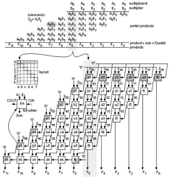
FIGURE 2.26 Multiplication. A 6-bit array multiplier using a final carry-propagate adder (full-adder cells a6 f6, a ripple-carry adder). Apart from the generation of the summands this multiplier uses the same structure as the carry-save adder of
Figure 2.23(d).
Suppose we wish to multiply 15 (the multiplicand ) by 19 (the multiplier ) mentally. It is easier to calculate 15 ¥ 20 and subtract 15. In effect we complete the multiplication as 15 ¥ (20 1) and we could write this as 15 ¥ 2 1 , with the overbar representing a minus sign. Now suppose we wish to multiply an 8-bit binary number, A, by B = 00010111 (decimal 16 + 4 + 2 + 1 = 23). It is easier to multiply A by the canonical signed-digit vector ( CSD vector ) D = 0010 1 001 (decimal 32 8 + 1 = 23) since this requires only three add or subtract operations (and a subtraction is as easy as an addition). We say B has a weight of 4 and D has a weight of 3. By using D instead of B we have reduced the number of partial products by 1 (= 4 3).
We can recode (or encode) any binary number, B, as a CSD vector, D, as follows (canonical means there is only one CSD vector for any number):
D i = B i + C i 2Ci + 1 , (2.58)
where C i + 1 is the carry from the sum of B i + 1 + B i + C i (we start with C 0 = 0).
As another example, if B = 011 (B 2 = 0, B 1 = 1, B 0 = 1; decimal 3), then, using Eq. 2.58,
D 0 = B 0 + C 0 2C1 = 1 + 0 2 = 1 ,
D 1 = B 1 + C 1 2C2 = 1 + 1 2 = 0,
D 2 = B 2 + C 2 2C3 = 0 + 1 0 = 1, (2.59)
so that D = 10 1 (decimal 4 1 = 3). CSD vectors are useful to represent fixed coefficients in digital filters, for example.
We can recode using a radix other than 2. Suppose B is an ( n + 1)-digit two s complement number,
B = B 0 + B 1 2 + B 2 2 2 + . . . + B i 2 i + . . . + B n 1 2 n 1 Bn 2 n . (2.60)
We can rewrite the expression for B using the following sleight-of-hand:
B = B0 + (B 0 B1 )2 + . . . + (B i 1 Bi )2 i + . . . + B n 1 2 n 1 |
Bn |
2B B= |
|
2 n |
|
= ( 2B1 + B 0 )2 0 + ( 2B3 + B 2 + B 1 )2 2 + . . . |
|
+ ( 2Bi + B i 1 + B i 2 )2 i 1 + ( 2Bi + 2 + B i + 1 + B i )2 i + 1 + . . . |
|
+ ( 2Bn + B i 1 + B i 2 )2 n 1 . |
(2.61) |
This is very useful. Consider B = 101001 (decimal 9 32 = 23, n = 5), B = 101001
= ( 2B1 + B 0 )2 0 + ( 2B3 + B 2 + B 1 )2 2 + ( 2B5 + B 4 + B 3 )2 4
(( 2 ¥ 0) + 1)20 + (( 2 ¥ 1) + 0 + 0)22 + (( 2 ¥ 1) + 0 + 1)24 . (2.62)
Equation 2.61 tells us how to encode B as a radix-4 signed digit, E = 12 1 (decimal 168 + 1 = 23). To multiply by B encoded as E we only have to perform a multiplication by 2 (a shift) and three add/subtract operations.
Using Eq. 2.61 we can encode any number by taking groups of three bits at a time and calculating
E j = 2Bi + B i 1 + B i 2 ,
E j + 1 = 2Bi + 2 + B i + 1 + B i , . . . , (2.63)
where each 3-bit group overlaps by one bit. We pad B with a zero, B n . . . B 1 B 0 0, to match the first term in Eq. 2.61. If B has an odd number of bits, then we extend the sign: B n B n . . . B 1 B 0 0. For example, B = 01011 (eleven), encodes to E = 1 11 (16 4 1); and B = 101 is E = 1 1. This is called Booth encoding and reduces the number of partial products by a factor of two and thus considerably reduces the area as well as increasing the speed of our multiplier [Booth, 1951].
Next we turn our attention to improving the speed of addition in the CSA array.
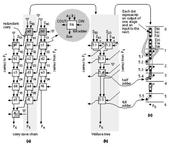
Figure 2.28(a) shows a section of the 6-bit array multiplier from Figure 2.27. We can collapse the chain of adders a0 f5 (5 adder delays) to the Wallace tree consisting of adders 5.1 5.4 (4 adder delays) shown in Figure 2.28(b).
FIGURE 2.27 Tree-based multiplication. (a) The portion of Figure 2.27 that calculates the sum bit, P 5 , using a chain of adders (cells a0 f5). (b) We can collapse this chain to a Wallace tree (cells 5.1 5.5). (c) The stages of multiplication.
Figure 2.28(c) pictorially represents multiplication as a sort of golf course. Each link corresponds to an adder. The holes or dots are the outputs of one stage (and the inputs of the next). At each stage we have the following three choices: (1) sum three outputs using a full adder (denoted by a box enclosing three dots); (2) sum two outputs using a half adder (a box with two dots); (3) pass the outputs directly to the next stage. The two outputs of an adder are joined by a diagonal line (full adders use black dots, half adders white dots). The object of the game is to choose (1), (2), or (3) at each stage to maximize the performance of the multiplier. In tree-based multipliers there are two ways to do this working forward and working backward.
In a Wallace-tree multiplier we work forward from the multiplier inputs, compressing the number of signals to be added at each stage [Wallace, 1960]. We can view an FA as a 3:2 compressor or (3, 2) counter it counts the number of '1's on the inputs. Thus, for example, an input of '101' (two '1's) results in an output '10' (2). A half adder is a (2, 2) counter . To form P 5 in Figure 2.29 we must add 6 summands (S 05 , S 14 , S 23 , S 32 , S 41 , and S 50 ) and 4 carries from the P 4 column. We add these in stages 1 7, compressing from 6:3:2:2:3:1:1. Notice that we wait until stage 5 to add the last carry
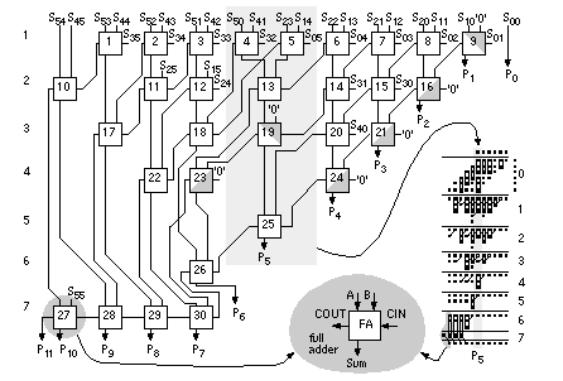
from column P 4 , and this means we expand (rather than compress) the number of signals (from 2 to 3) between stages 3 and 5. The maximum delay through the CSA array of Figure 2.29 is 6 adder delays. To this we must add the delay of the 4-bit (9 inputs) CPA (stage 7). There are 26 adders (6 half adders) plus the 4 adders in the CPA.
FIGURE 2.28 A 6-bit Wallace-tree multiplier. The carry-save adder (CSA) requires 26 adders (cells 1 26, six are half adders). The final carry-propagate adder (CPA) consists of 4 adder cells (27 30). The delay of the CSA is 6 adders. The delay of the CPA is 4 adders.
In a Dadda multiplier (Figure 2.30) we work backward from the final product [Dadda, 1965]. Each stage has a maximum of 2, 3, 4, 6, 9, 13, 19, . . . outputs (each successive stage is 3/2 times larger rounded down to an integer). Thus, for example, in
Figure 2.28(d) we require 3 stages (with 3 adder delays plus the delay of a 10-bit output CPA) for a 6-bit Dadda multiplier. There are 19 adders (4 half adders) in the CSA plus the 10 adders (2 half adders) in the CPA. A Dadda multiplier is usually faster and smaller than a Wallace-tree multiplier.
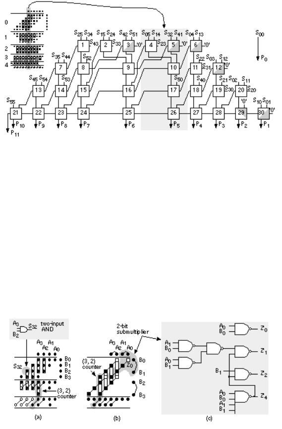
FIGURE 2.29 The 6-bit Dadda multiplier. The carry-save adder (CSA) requires 20 adders (cells 1 20, four are half adders). The carry-propagate adder (CPA, cells 21 30) is a ripple-carry adder (RCA). The CSA is smaller (20 versus 26 adders), faster (3 adder delays versus 6 adder delays), and more regular than the Wallace-tree CSA of Figure 2.29. The overall speed of this implementation is approximately the same as the Wallace-tree multiplier of Figure 2.29; however, the speed may be increased by substituting a faster CPA.
In general, the number of stages and thus delay (in units of an FA delay excluding the CPA) for an n -bit tree-based multiplier using (3, 2) counters is
log 1.5 n = log 10 n /log 10 1.5 = log 10 n /0.176 . (2.64)
Figure 2.31(a) shows how the partial-product array is constructed in a conventional 4-bit multiplier. The Ferrari Stefanelli multiplier (Figure 2.31b) nests multipliers the 2-bit submultipliers reduce the number of partial products [Ferrari and Stefanelli, 1969].
FIGURE 2.30 Ferrari Stefanelli multiplier. (a) A conventional 4-bit array multiplier using AND gates to calculate the summands with (2, 2) and (3, 2) counters to sum the partial products. (b) A 4-bit Ferrari Stefanelli multiplier using 2-bit submultipliers to construct the partial product array. (c) A circuit implementation for an inverting 2-bit submultiplier.
There are several issues in deciding between parallel multiplier architectures:
1.Since it is easier to fold triangles rather than trapezoids into squares, a Wallace-tree multiplier is more suited to full-custom layout, but is slightly larger, than a Dadda multiplier both are less regular than an array multiplier. For cell-based ASICs, a Dadda multiplier is smaller than a Wallace-tree multiplier.
2.The overall multiplier speed does depend on the size and architecture of the final CPA, but this may be optimized independently of the CSA array. This means a Dadda multiplier is always at least as fast as the Wallace-tree version.
3.The low-order bits of any parallel multiplier settle first and can be added in the CPA before the remaining bits settle. This allows multiplication and the final addition to be overlapped in time.
4.Any of the parallel multiplier architectures may be pipelined. We may also use a variably pipelined approach that tailors the register locations to the size of the multiplier.
5.Using (4, 2), (5, 3), (7, 3), or (15, 4) counters increases the stage compression and permits the size of the stages to be tuned. Some ASIC cell libraries contain a (7, 3) counter a 2-bit full-adder . A (15, 4) counter is a 3-bit full adder. There is a trade-off in using these counters between the speed and size of the logic cells and the delay as well as area of the interconnect.
6.Power dissipation is reduced by the tree-based structures. The simplified carry-save logic produces fewer signal transitions and the tree structures produce fewer glitches than a chain.
7.None of the multiplier structures we have discussed take into account the possibility of staggered arrival times for different bits of the multiplicand or the multiplier. Optimization then requires a logic-synthesis tool.
2.6.5 Other Arithmetic Systems
There are other schemes for addition and multiplication that are useful in special circumstances. Addition of numbers using redundant binary encoding avoids carry propagation and is thus potentially very fast. Table 2.13 shows the rules for addition using an intermediate carry and sum that are added without the need for carry. For example,
binary |
decimal redundant binary CSD vector |
|
||||
1010111 |
87 |
10101001 |
10 1 0 1 00 1 |
addend |
||
+ 1100101 |
101 |
+ 11100111 |
+ 01100101 |
augend |
||
|
|
|
01001110 |
= 11 00 1 100 |
intermediate sum |
|
|
|
|
1 1 00010 1 |
11000000 |
intermediate carry |
|
= 10111100 = 188 |
1 1 1000 1 00 |
10 1 00 1 100 |
sum |
|||
TABLE 2.13 Redundant binary addition. |
|
|||||
A[ i ] B[ i ] A[ i 1] |
B[ i 1] |
Intermediate Intermediate |
||||
sum |
carry |
|||||
|
|
|
|
|||
1 |
1 |
x |
x |
0 |
1 |
|
1 |
0 |
A[i 1]=0/1 and B[i 1]=0/1 1 |
0 |
|||
0 |
1 |
A[i 1]= 1 or B[i 1]= 1 |
1 |
1 |
|
1 |
1 |
x |
x |
0 |
0 |
1 |
1 |
x |
x |
0 |
0 |
0 |
0 |
x |
x |
0 |
0 |
0 |
1 |
A[i 1]=0/1 and B[i 1]=0/1 1 |
1 |
||
1 |
0 |
A[i 1]= 1 or B[i 1]= 1 |
1 |
0 |
|
1 |
1 |
x |
x |
0 |
1 |
The redundant binary representation is not unique. We can represent 101 (decimal), for example, by 1100101 (binary and CSD vector) or 1 1 100111. As another example, 188 (decimal) can be represented by 10111100 (binary), 1 1 1000 1 00, 10 1 00 1 100, or 10 1 000 1 00 (CSD vector). Redundant binary addition of binary, redundant binary, or CSD vectors does not result in a unique sum, and addition of two CSD vectors does not result in a CSD vector. Each n -bit redundant binary number requires a rather wasteful 2 n -bit binary number for storage. Thus 10 1 is represented as 010010, for example (using sign magnitude). The other disadvantage of redundant binary arithmetic is the need to convert to and from binary representation.
Table 2.14 shows the (5, 3) residue number system . As an example, 11 (decimal) is represented as [1, 2] residue (5, 3) since 11R 5 = 11 mod 5 = 1 and 11R 3 = 11 mod 3 = 2. The size of this system is thus 3 ¥ 5 = 15. We add, subtract, or multiply residue numbers using the modulus of each bit position without any carry. Thus:
4 |
[4, 1] |
12 |
[2, 0] |
3 |
|
[3, 0] |
+ 7 |
+ [2, 1] |
4 |
- [4, 1] |
¥ |
4 |
¥ [4, 1] |
= 11 |
= [1, 2] |
= 8 |
= [3, 2] |
= 12 |
= [2, 0] |
|
TABLE 2.14 The 5, 3 residue number system. |
|
|||||
n residue 5 residue 3 n residue 5 residue 3 n |
residue 5 residue 3 |
|||||
0 0 |
0 |
5 0 |
2 |
10 |
0 |
1 |
1 1 |
1 |
6 1 |
0 |
11 |
1 |
2 |
2 2 |
2 |
7 2 |
1 |
12 |
2 |
0 |
3 3 |
0 |
8 3 |
2 |
13 |
3 |
1 |
4 4 |
1 |
9 4 |
0 |
14 |
4 |
2 |
The choice of moduli determines the system size and the computing complexity. The most useful choices are relative primes (such as 3 and 5). With p prime, numbers of the form 2 p and 2 p 1 are particularly useful (2p 1 are Mersenne s numbers ) [Waser and Flynn, 1982].
2.6.6 Other Datapath Operators
Figure 2.32 shows symbols for some other datapath elements. The combinational datapath cells, NAND, NOR, and so on, and sequential datapath cells (flip-flops and latches) have standard-cell equivalents and function identically. I use a bold outline (1 point) for datapath cells instead of the regular (0.5 point) line I use for scalar symbols. We call a set of identical cells a vector of datapath elements in the same way that a bold symbol, A , represents a vector and A represents a scalar.
FIGURE 2.31 Symbols for datapath elements. (a) An array or vector of flip-flops (a register). (b) A two-input NAND cell with databus inputs. (c) A two-input NAND cell with a control input. (d) A buswide MUX. (e) An incrementer/decrementer. (f) An all-zeros detector. (g) An all-ones detector. (h) An adder/subtracter.
A subtracter is similar to an adder, except in a full subtracter we have a borrow-in signal, BIN; a borrow-out signal, BOUT; and a difference signal, DIFF:
DIFF |
= A • NOT(B) • NOT( BIN) |
|
|
SUM(A, NOT(B), NOT(BIN)) |
(2.65) |
NOT(BOUT) = A · NOT(B) + A · NOT(BIN) + NOT(B) · NOT(BIN) |
|
|
|
MAJ(NOT(A), B, NOT(BIN)) |
(2.66) |
These equations are the same as those for the FA (Eqs. 2.38 and 2.39) except that the B input is inverted and the sense of the carry chain is inverted. To build a subtracter that calculates (A B) we invert the entire B input bus and connect the BIN[0] input to VDD (not to VSS as we did for CIN[0] in an adder). As an example, to subtract B = '0011' from A = '1001' we calculate '1001' + '1100' + '1' = '0110'. As with an adder, the true overflow is XOR(BOUT[MSB], BOUT[MSB 1]).
We can build a ripple-borrow subtracter (a type of borrow-propagate subtracter), a borrow-save subtracter, and a borrow-select subtracter in the same way we built these adder architectures. An adder/subtracter has a control signal that gates the A input with an exclusive-OR cell (forming a programmable inversion) to switch between an adder or subtracter. Some adder/subtracters gate both inputs to allow us to compute ( A B). We must be careful to connect the input to the LSB of the carry chain (CIN[0] or BIN[0]) when changing between addition (connect to VSS) and subtraction (connect to VDD).
A barrel shifter rotates or shifts an input bus by a specified amount. For example if we have an eight-input barrel shifter with input '1111 0000' and we specify a shift of '0001 0000' (3, coded by bit position) the right-shifted 8-bit output is '0001 1110'. A barrel shifter may rotate left or right (or switch between the two under a separate control). A barrel shifter may also have an output width that is smaller than the input. To use a simple example, we may have an 8-bit input and a 4-bit output. This situation is equivalent to having a barrel shifter with two 4-bit inputs and a 4-bit output. Barrel
shifters are used extensively in floating-point arithmetic to align (we call this normalize and denormalize ) floating-point numbers (with sign, exponent, and mantissa).
A leading-one detector is used with a normalizing (left-shift) barrel shifter to align mantissas in floating-point numbers. The input is an n -bit bus A, the output is an n -bit bus, S, with a single '1' in the bit position corresponding to the most significant '1' in the input. Thus, for example, if the input is A = '0000 0101' the leading-one detector output is S = '0000 0100', indicating the leading one in A is in bit position 2 (bit 7 is the MSB, bit zero is the LSB). If we feed the output, S, of the leading-one detector to the shift select input of a normalizing (left-shift) barrel shifter, the shifter will normalize the input A. In our example, with an input of A = '0000 0101', and a left-shift of S = '0000 0100', the barrel shifter will shift A left by five bits and the output of the shifter is Z = '1010 0000'. Now that Z is aligned (with the MSB equal to '1') we can multiply Z with another normalized number.
The output of a priority encoder is the binary-encoded position of the leading one in an input. For example, with an input A = '0000 0101' the leading 1 is in bit position 3 (MSB is bit position 7) so the output of a 4-bit priority encoder would be Z = '0011' (3). In some cell libraries the encoding is reversed so that the MSB has an output code of zero, in this case Z = '0101' (5). This second, reversed, encoding scheme is useful in floating-point arithmetic. If A is a mantissa and we normalize A to '1010 0000' we have to subtract 5 from the exponent, this exponent correction is equal to the output of the priority encoder.
An accumulator is an adder/subtracter and a register. Sometimes these are combined with a multiplier to form a multiplier accumulator ( MAC ). An incrementer adds 1 to the input bus, Z = A + 1, so we can use this function, together with a register, to negate a two s complement number for example. The implementation is Z[ i ] = XOR(A[ i ], CIN[ i ]), and COUT[ i ] = AND(A[ i ], CIN[ i ]). The carry-in control input, CIN[0], thus acts as an enable: If it is set to '0' the output is the same as the input.
The implementation of arithmetic cells is often a little more complicated than we have explained. CMOS logic is naturally inverting, so that it is faster to implement an incrementer as
Z[ i (even)] = XOR(A[ i ], CIN[ i ]) and COUT[ i (even)] = NAND(A[ i ], CIN[ i ]).
This inverts COUT, so that in the following stage we must invert it again. If we push an inverting bubble to the input CIN we find that:
Z[ i (odd)] = XNOR(A[ i ], CIN[ i ]) and COUT[ i (even)] = NOR(NOT(A[ i ]), CIN[ i ]).
In many datapath implementations all odd-bit cells operate on inverted carry signals, and thus the odd-bit and even-bit datapath elements are different. In fact, all the adder and subtracter datapath elements we have described may use this technique. Normally this is completely hidden from the designer in the datapath assembly and any output control signals are inverted, if necessary, by inserting buffers.
A decrementer subtracts 1 from the input bus, the logical implementation is Z[ i ] = XOR(A[ i ], CIN[ i ]) and COUT[ i ] = AND(NOT(A[ i ]), CIN[ i ]). The implementation may invert the odd carry signals, with CIN[0] again acting as an enable.
An incrementer/decrementer has a second control input that gates the input, inverting

the input to the carry chain. This has the effect of selecting either the increment or decrement function.
Using the all-zeros detectors and all-ones detectors , remember that, for a 4-bit number, for example, zero in ones complement arithmetic is '1111' or '0000', and that zero in signed magnitude arithmetic is '1000' or '0000'.
A register file (or scratchpad memory) is a bank of flip-flops arranged across the bus; sometimes these have the option of multiple ports (multiport register files) for read and write. Normally these register files are the densest logic and hardest to fit in a datapath. For large register files it may be more appropriate to use a multiport memory. We can add control logic to a register file to create a first-in first-out register ( FIFO ), or last-in first-out register ( LIFO ).
In Section 2.5 we saw that the standard-cell version and gate-array macro version of the sequential cells (latches and flip-flops) each contain their own clock buffers. The reason for this is that (without intelligent placement software) we do not know where a standard cell or a gate-array macro will be placed on a chip. We also have no idea of the condition of the clock signal coming into a sequential cell. The ability to place the clock buffers outside the sequential cells in a datapath gives us more flexibility and saves space. For example, we can place the clock buffers for all the clocked elements at the top of the datapath (together with the buffers for the control signals) and river route (in river routing the interconnect lines all flow in the same direction on the same layer) the connections to the clock lines. This saves space and allows us to guarantee the clock skew and timing. It may mean, however, that there is a fixed overhead associated with a datapath. For example, it might make no sense to build a 4-bit datapath if the clock and control buffers take up twice the space of the datapath logic. Some tools allow us to design logic using a portable netlist . After we complete the design we can decide whether to implement the portable netlist in a datapath, standard cells, or even a gate array, based on area, speed, or power considerations.
2.7 I/O Cells
Figure 2.33 shows a three-state bidirectional output buffer (Tri-State ® is a registered trademark of National Semiconductor). When the output enable (OE) signal is high, the circuit functions as a noninverting buffer driving the value of DATAin onto the I/O pad. When OE is low, the output transistors or drivers , M1 and M2, are disconnected. This allows multiple drivers to be connected on a bus. It is up to the designer to make sure that a bus never has two drivers a problem known as contention .
In order to prevent the problem opposite to contention a bus floating to an intermediate voltage when there are no bus drivers we can use a bus keeper or bus-hold cell (TI calls this Bus-Friendly logic). A bus keeper normally acts like two weak (low drive-strength) cross-coupled inverters that act as a latch to retain the last logic state on the bus, but the latch is weak enough that it may be driven easily to the opposite state. Even though bus keepers act like latches, and will simulate like latches, they should not be used as latches, since their drive strength is weak.
Transistors M1 and M2 in Figure 2.33 have to drive large off-chip loads. If we wish to change the voltage on a C = 200 pF load by 5 V in 5 ns (a slew rate of 1 Vns 1 ) we will require a current in the output transistors of I DS = C (d V /d t ) = (200 ¥ 10 12 ) (5/5 ¥ 10 9 ) = 0.2 A or 200 mA.
Such large currents flowing in the output transistors must also flow in the power supply bus and can cause problems. There is always some inductance in series with the power supply, between the point at which the supply enters the ASIC package and reaches the power bus on the chip. The inductance is due to the bond wire, lead frame, and package pin. If we have a power-supply inductance of 2 nH and a current changing from zero to 1 A (32 I/O cells on a bus switching at 30 mA each) in 5 ns, we will have a voltage spike on the power supply (called power-supply bounce ) of L (d I /d t ) = (2 ¥ 10 9 )(1/(5 ¥ 10 9 )) = 0.4 V.
We do several things to alleviate this problem: We can limit the number of simultaneously switching outputs (SSOs), we can limit the number of I/O drivers that can be attached to any one VDD and GND pad, and we can design the output buffer to limit the slew rate of the output (we call these slew-rate limited I/O pads). Quiet-I/O cells also use two separate power supplies and two sets of I/O drivers: an AC supply (clean or quiet supply) with small AC drivers for the I/O circuits that start and stop the output slewing at the beginning and end of a output transition, and a DC supply (noisy or dirty supply) for the transistors that handle
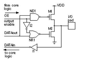
large currents as they slew the output.
The three-state buffer allows us to employ the same pad for input and output bidirectional I/O . When we want to use the pad as an input, we set OE low and take the data from DATAin. Of course, it is not necessary to have all these features on every pad: We can build output-only or input-only pads.
FIGURE 2.32 A three-state bidirectional output buffer. When the output enable, OE, is '1' the output section is enabled and drives the I/O pad. When OE is '0' the output buffer is placed in a high-impedance state.
We can also use many of these output cell features for input cells that have to drive large on-chip loads (a clock pad cell, for example). Some gate arrays simply turn an output buffer around to drive a grid of interconnect that supplies a clock signal internally. With a typical interconnect capacitance of 0.2pFcm 1 , a grid of 100 cm (consisting of 10 by 10 lines running all the way across a 1 cm chip) presents a load of 20 pF to the clock buffer.
Some libraries include I/O cells that have passive pull-ups or pull-downs (resistors) instead of the transistors, M1 and M2 (the resistors are normally still constructed from transistors with long gate lengths). We can also omit one of the driver transistors, M1 or M2, to form open-drain outputs that require an external pull-up or pull-down. We can design the output driver to produce TTL output levels rather than CMOS logic levels. We may also add input hysteresis (using a Schmitt trigger) to the input buffer, I1 in Figure 2.33, to accept input data signals that contain glitches (from bouncing switch contacts, for example) or that are slow rising. The input buffer can also include a level shifter to accept TTL input levels and shift the input signal to CMOS levels.
The gate oxide in CMOS transistors is extremely thin (100 Å or less). This leaves the gate oxide of the I/O cell input transistors susceptible to breakdown from static electricity ( electrostatic discharge , or ESD ). ESD arises when we or machines handle the package leads (like the shock I sometimes get when I touch a doorknob after walking across the carpet at work). Sometimes this problem is called electrical overstress (EOS) since most ESD-related failures are caused not by gate-oxide breakdown, but by the thermal stress (melting) that occurs when the n -channel transistor in an output driver overheats (melts) due to the large current that can flow in the drain diffusion connected to a pad during an ESD event.

To protect the I/O cells from ESD, the input pads are normally tied to device structures that clamp the input voltage to below the gate breakdown voltage (which can be as low as 10 V with a 100 Å gate oxide). Some I/O cells use transistors with a special ESD implant that increases breakdown voltage and provides protection. I/O driver transistors can also use elongated drain structures (ladder structures) and large drain-to-gate spacing to help limit current, but in a salicide process that lowers the drain resistance this is difficult. One solution is to mask the I/O cells during the salicide step. Another solution is to use pnpn and npnp diffusion structures called silicon-controlled rectifiers (SCRs) to clamp voltages and divert current to protect the I/O circuits from ESD.
There are several ways to model the capability of an I/O cell to withstand EOS. The human-body model ( HBM ) represents ESD by a 100 pF capacitor discharging through a 1.5 k W resistor (this is an International Electrotechnical Committee, IEC, specification). Typical voltages generated by the human body are in the range of 2 4 kV, and we often see an I/O pad cell rated by the voltage it can withstand using the HBM. The machine model ( MM ) represents an ESD event generated by automated machine handlers. Typical MM parameters use a 200 pF capacitor (typically charged to 200 V) discharged through a 25 W resistor, corresponding to a peak initial current of nearly 10 A. The charge-device model ( CDM , also called device charge discharge) represents the problem when an IC package is charged, in a shipping tube for example, and then grounded. If the maximum charge on a package is 3 nC (a typical measured figure) and the package capacitance to ground is 1.5 pF, we can simulate this event by charging a 1.5 pF capacitor to 2 kV and discharging it through a 1 W resistor.
If the diffusion structures in the I/O cells are not designed with care, it is possible to construct an SCR structure unwittingly, and instead of protecting the transistors the SCR can enter a mode where it is latched on and conducting large enough currents to destroy the chip. This failure mode is called latch-up . Latch-up can occur if the pn -diodes on a chip become forward-biased and inject minority carriers (electrons in p -type material, holes in n -type material) into the substrate. The source substrate and drain substrate diodes can become forward-biased due to power-supply bounce or output undershoot (the cell outputs fall below V SS ) or overshoot (outputs rise to greater than V DD ) for example. These injected minority carriers can travel fairly large distances and interact with nearby transistors causing latch-up. I/O cells normally surround the I/O transistors with guard rings (a continuous ring of n -diffusion in an n -well connected to VDD, and a ring of p -diffusion in a p -well connected to VSS) to collect these minority carriers. This is a problem that can also occur in the logic core and this is one reason that we normally include substrate and well connections to the power supplies in every cell.

2.8 Cell Compilers
The process of hand crafting circuits and layout for a full-custom IC is a tedious, time-consuming, and error-prone task. There are two types of automated layout assembly tools, often known as a silicon compilers . The first type produces a specific kind of circuit, a RAM compiler or multiplier compiler , for example. The second type of compiler is more flexible, usually providing a programming language that assembles or tiles layout from an input command file, but this is full-custom IC design.
We can build a register file from latches or flip-flops, but, at 4.5 6.5 gates (18 26 transistors) per bit, this is an expensive way to build memory. Dynamic RAM (DRAM) can use a cell with only one transistor, storing charge on a capacitor that has to be periodically refreshed as the charge leaks away. ASIC RAM is invariably static (SRAM), so we do not need to refresh the bits. When we refer to RAM in an ASIC environment we almost always mean SRAM. Most ASIC RAMs use a six-transistor cell (four transistors to form two cross-coupled inverters that form the storage loop, and two more transistors to allow us to read from and write to the cell). RAM compilers are available that produce single-port RAM (a single shared bus for read and write) as well as dual-port RAMs , and multiport RAMs . In a multi-port RAM the compiler may or may not handle the problem of address contention (attempts to read and write to the same RAM address simultaneously). RAM can be asynchronous (the read and write cycles are triggered by control and/or address transitions asynchronous to a clock) or synchronous (using the system clock).
In addition to producing layout we also need a model compiler so that we can verify the circuit at the behavioral level, and we need a netlist from a netlist compiler so that we can simulate the circuit and verify that it works correctly at the structural level. Silicon compilers are thus complex pieces of software. We assume that a silicon compiler will produce working silicon even if every configuration has not been tested. This is still ASIC design, but now we are relying on the fact that the tool works correctly and therefore the compiled blocks are correct by construction .

2.9 Summary
The most important concepts that we covered in this chapter are the following:
●The use of transistors as switches
●The difference between flip-flop and a latch
●The meaning of setup time and hold time
●Pipelines and latency
●The difference between datapath, standard-cell, and gate-array logic cells
●Strong and weak logic levels
●Pushing bubbles
●Ratio of logic
●Resistance per square of layers and their relative values in CMOS
●Design rules and l
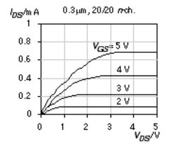
2.10 Problems
* = Difficult,** = Very difficult, *** = Extremely difficult
2.1(Switches, 20 min.) (a) Draw a circuit schematic for a two-way light switch: flipping the switch at the top or bottom of the stairs reverses the state of two light bulbs, one at the top and one at the bottom of the stairs. Your schematic should show and label all the cables, switches, and bulbs. (b) Repeat the problem for three switches and one light in a warehouse.
2.2(Logic, 10 min.) The queen wished to choose her successor wisely. She blindfolded and then placed a crown on each of her three children, explaining that there were three red and two blue crowns, and they must deduce the color of their own crown. With blindfolds removed the children could see the two other crowns, but not their own. After a while Anne said: My crown is red. How did she know?
2.3(Minus signs, 20 min.) The channel charge in an n -channel transistor is negative. (a) Should there not be a minus sign in Eq. 2.5 to account for this? (b) If so, then where in the derivation of Section 2.1 does the minus sign disappear to arrive at Eq. 2.9 for the current in an n -channel transistor? (c) The equations for the current in a p -channel transistor (Eq. 2.15) have the opposite sign to those for an n -channel transistor. Where in the derivation in Section 2.1 does the extra minus sign arise?
FIGURE 2.33 Transistor characteristics for a
0.3m m process (Problem 2.4).
2.4(Transistor curves, 20 min.) Figure 2.34 shows the measured I DS V DS
characteristics for a 20/20 n -channel transistor in a 0.3 m m (effective gate length) process from an ASIC foundry. Derive as much information as you can from this figure.
2.5 (Body effect, 20 min). The equations for the drain source current (2.9, 2.12,
and 2.15) do not contain V SB , the source voltage with respect to the bulk, because we assumed that it was zero. This is not true for the n -channel transistor whose drain is connected to the output in a two-input NAND gate, for example. A reverse substrate bias (or back-gate bias; V SB > 0 for an n -channel transistor) makes the bulk act like a second gate (the back gate) and modifies an n -channel transistor threshold voltage as follows:
V tn = V t0 n + g [ ( f 0 + V SB ) f0 ] , (2.67)
where V t 0 n is measured with V SB = 0 V; f 0 is called the surface potential; and g (gamma) is the body-effect coefficient (back-gate bias coefficient),
g = (2q e Si N A )/C ox . (2.68)
There are several alternative names and symbols for f 0 ( phi, a positive quantity for an n -channel transistor, typically between 0.6 0.7 V) you may also see fb (for bulk potential) or 2 f F (twice the Fermi potential, a negative quantity). In
Eq. 2.68, e Si = e 0 e r = 1.053 ¥ 10 10 Fm 1 is the permittivity of silicon (the permittivity of a vacuum e 0 = 8.85 ¥ 10 12 Fm 1 and the relative permittivity of silicon is e r = 11.7); N A is the acceptor doping concentration in the bulk (for p -type substrate or well N D for the donor concentration in an n -type substrate or well); and C ox is the gate capacitance per unit area given by
Cox = e ox /T ox . (2.69)
●a. Calculate the theoretical value of g for N A = 10 16 cm 3 , T ox = 100 Å.
●b. Calculate and plot V t n for V SB ranging from 0 V to 5 V in increments of 1 V assuming values of g = 0.5 V 0.5 , f 0 = 0.6 V, and V t0 n = 0.5 V obtained from transistor characteristics.
●c. Fit a linear approximation to V t n .
●d. Recognizing V SB £ 0 V, rewrite Eq. 2.67 for a p -channel device.
●e. (Harder) What effect does the back-gate bias effect have on CMOS logic circuits?
Answer: (a) 0.17 V 0.5 (b) 0.50 1.3 V.
2.6(Sizing layout, 10 min.) Stating clearly whatever assumptions you make and describing the tools and methods you use, estimate the size (in l ) of the standard cell shown in Figure 1.3. Estimate the size of each of the transistors, giving their channel lengths and widths (stating clearly which is which).
2.7(CMOS process) (20 min.) Table 2.15 shows the major steps involved in a typical deep submicron CMOS process. There are approximately 100 major steps in the process.
●a. If each major step has a yield of 0.9, what is the overall process yield?
●b. If the process yield is 90 % (not uncommon), what is the average yield at each major step?
●c. If each of the major steps in Table 2.15 consists of an average of five other microtasks, what is the average yield of each of the 500 microtasks.
●d. Suppose, for example, an operator loads and unloads a furnace five times a day as a microtask, how many days must the operator work without making a mistake to achieve this microtask yield?
●e. Does this seem reasonable? What is wrong with our model?
●f. (**60 min.) Draw the process cross-section showing, in particular, the poly, FOX, gate oxide, IMOs and metal layers. You may have to make some assumptions about the meanings and functions of the various steps and layers. Assume all layers are deposited on top of each other according to the thicknesses shown (do not attempt to correct for the silicon consumed during oxidation even if you understand what this means). The abbreviations in Table 2.15 are as follows: dep. = deposition; LPCVD = low-pressure chemical vapor deposition (for growing oxide and poly); LDD = lightly doped drain (a way to improve transistor characteristics); SOG = silicon overglass (a deposited quartz to help with step coverage between metal layers).
TABLE 2.15 CMOS process steps (Problem 2.7). 1 |
|
||||||
|
Step |
Depth |
Step |
Depth |
|
Step |
Depth |
1 |
substrate |
|
32 resist strip |
|
63 m1 mask |
|
|
2 |
oxide 1 dep. |
500 |
33 WSi anneal |
|
64 m1 etch |
|
|
3 |
nitride 1 |
1500 |
34 nLDD mask |
|
65 resist strip |
|
|
dep. |
|
|
|||||
|
|
|
|
|
|
base oxide |
|
4 |
n-well mask |
|
35 nLDD implant |
|
66 dep. |
6000 |
|
5 |
n-well etch |
|
36 resist strip |
|
67 SOG coat1/2 |
3000 |
|
6 |
n-well |
|
|
|
|
SOG |
|
implant |
|
37 pLDD mask |
|
68 cure/etch |
4000 |
||
|
|
|
|
|
|
cap oxide |
|
7 |
resist strip |
|
38 pLDD implant |
|
69 dep. |
4000 |
|
8 |
blocking |
2000 |
39 resist strip |
|
70 via1 mask |
|
|
oxide dep. |
|
|
|||||
9 |
nitride 1 |
|
40 spacer oxide |
3000 |
71 via1 etch |
2500 |
|
|
strip |
|
dep. |
|
|
|
|
|
p-well |
|
|
|
|
|
|
10 implant |
|
41 WSi anneal |
|
72 resist strip |
|
||
11 p-well drive |
|
42 SD oxide dep |
200 |
73 TiW dep. |
2000 |
||
|
active oxide |
|
|
|
|
AlCu/TiW |
|
12 dep. |
250 |
43 n+ mask |
|
74 dep. |
4000 |
||
13 nitride 2 |
1500 |
44 n+ implant |
|
75 m2 mask |
dep. |
|
|
|
|
14 active mask |
|
45 resist strip |
|
76 m2 etch |
15 active etch |
|
46 ESD mask |
|
77 resist strip |
16 resist strip |
|
47 ESD implant |
|
78 base oxide |
|
|
|
|
dep. |
17 field mask |
|
48 resist strip |
|
79 SOG coat 1/2 |
18 field implant |
|
49 p+ mask |
|
80 SOG |
|
|
|
|
cure/etch |
19 resist strip |
|
50 p+ implant |
|
81 cap oxide |
|
|
|
|
dep. |
20 field oxide |
5000 |
51 resist strip |
|
82 via2 mask |
dep. |
|
|
|
|
21 nitride 2 |
|
52 implant anneal |
|
83 via2 etch |
strip |
|
|
|
|
22 sacrificial |
300 |
53 LPCVD oxide |
1500 |
84 resist strip |
oxide dep. |
|
dep. |
|
|
Vt adjust |
|
BPSG |
|
|
23 implant |
|
54 dep./densify |
4000 |
85 TiW dep. |
24 gate oxide |
80 |
55 contact mask |
|
86 AlCu/TiW |
dep. |
|
|
|
dep. |
25 LPCVD |
1500 |
56 contact etch |
2500 |
87 m3 mask |
poly dep. |
|
|
|
|
26 deglaze |
|
57 resist strip |
|
88 m3 etch |
27 WSi dep. |
1500 |
58 Pt dep. |
200 |
89 resist strip |
LPCVD |
|
|
|
|
28 oxide dep. |
750 |
59 Pt sinter |
|
90 oxide dep. |
29 poly mask |
|
60 Pt strip |
|
92 nitride dep. |
30 oxide etch |
|
61 TiW dep. |
2000 |
93 pad mask |
polycide |
|
|
|
|
31 etch |
|
62 AlCu/TiW dep. |
4000 |
94 pad etch |
6000
3000
4000
4000
2500
2000
4000
4000
10,000
Answer: (a) Zero. (b) 0.999. (c) 0.9998. (d) 3 years.
2.8(Stipple patterns, 30 min.)
●a. Check the stipple patterns in Figure 2.9. Using ruled paper draw 8-by-8 stipple patterns for all the combinations of layers shown.
●b. Repeat part a for Figure 2.10.
2.9(Select, 20 min.) Can you draw a design-rule correct (according to the design rules in Tables 2.7 2.9) layout with a piece of select that has a minimum width of 2 l (rule 4.4)?
2.10 (*Inverter layout, 60 min.) Using 1/4-inch ruled paper (or similar) draw a minimum-size inverter (W/L = 1 for both p -channel and n -channel transistors). Use a scale of one square to 2 l and the design rules in Table 2.7 Table 2.9. Do not use m2 or m3 only m1. Draw the nwell, pwell, ndiff, and pdiff layers, but not the implant layers or the active layer. Include connections to the input, output, VDD, and VSS in m1. There must be at least one well connection to each well ( n -well to VDD, and p -well to VSS). Minimize the size of your cell BB. Draw the BB outline and write its size in l 2 on your drawing. Use green diagonal stripes for ndiff, brown diagonal stripes for pdiff, red diagonal stripes for poly, blue diagonal stripes for m1, solid black for contact). Include a key on your drawing, and clearly label the input, output, VDD, and VSS contacts.
2.11 (*AOI221 Layout, 120 min.) Layout the AOI221 shown in Figure 2.13 with the design rules of Tables 2.7 2.9 and using Figure 1.3 as a guide. Label clearly the m1 corresponding to the inputs, output, VDD bus, and GND (VSS) bus. Remember to include substrate contacts. What is the size of your BB in l 2 ?
2.12(Resistance, 20 min.)
●a. Using the values for sheet resistance shown in Table 2.3, calculate the resistance of a 200 l long (in the direction of current flow) by 3 l wide piece of each of the layers.
●b. Estimate the resistance of an 8-inch, 10 W cm, p -type, <100> wafer, measured (i) from edge to edge across a diameter and (ii) from face center to the face center on the other side.
2.13(*Layout graphics, 120 min.) Write a tutorial for capturing layout. As an example:
To capture EPSF (encapsulated PostScript format) from Tanner Research s L-Edit for documentation, Macintosh version... Create a black-and-white technology file, use Setup, Layers..., in L-Edit. The method described here does not work well for grayscale or color. Use File, Print..., Destination check button File to print from L-Edit to an EPS (encapsulated PostScript) file. After you choose Save, a dialog box appears. Select Format: EPS Enhanced Mac Preview, ASCII, Level 1 Compatible, Font Inclusion: None. Save the file. Switch to Frame. Create an Anchored Frame. Use File, Import, File... to bring up a dialog box. Check button Copy into Document, select Format: EPSF. Import the EPS file that will appear as a page image . Grab the graphic inside the Anchored Frame and move the page image around. There will be a footer with text on thepage image that you may want to hide by using the Anchored Frame edges to crop the image.
Your instructions should be precise, concise, assume nothing, and use the names of menu items, buttons and so on exactly as they appear to the user. Most of the layout figures in this book were created using L-Edit running on a Macintosh, with labels added in FrameMaker. Most of the layouts use the Compass layout editor.
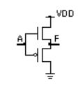
2.14 (Transistor resistance, 20 min.) Calculate I DS and the resistance (the DC value V DS / I DS as well as the AC value V DS / I DS as appropriate) of long-channel transistors with the following parameters, under the specified conditions. In each case state whether the transistor is in the saturation region, linear region, or off:
(i) n -channel: V t n = 0.5 V, b n = 40 m AV 2 :
V GS = 3.3V: a. V DS = 3.3 V b. V DS = 0.0 V c. V GS = 0.0 V, V DS = 3.3 V
(ii) p -channel: V t p = 0.6 V, b p = 20 m AV 2 :
V GS = 0.0 V: a. V DS = 0.0 V b. V DS = 5.0 V c. V GS = 5.0 V, V DS = 5.0 V
2.15 (Circuit theory, 15 min.) You accidentally created the inverter shown in Figure 2.35 on a full-custom ASIC currently being fabricated. Will it work? Your manager wants a yes or no answer. Your group is a little more understanding: You are to make a presentation to them to explain the problems ahead. Prepare two foils as well as a one page list of alternatives and recommendations.
FIGURE 2.34 A CMOS inverter with n -channel and p -channel transistors swapped (Problem 2.15).
2.16(Mask resolution, 10 min.) People use LaserWriters to make printed-circuit boards all the time.
●a. Do you think it is possible to make an IC mask using a 600 dpi (dots per inch) LaserWriter and a transparency?
●b. What would l be?
●c. (Harder) See if you can use a microscope to look at the dot and the rectangular bars (serifs) of a letter 'i' from the output of a LaserWriter on paper (most are 300 dpi or 600 dpi). Estimate l . What is causing the problem? Why is there no rush to generate 1200 dpi LaserWriters for paper? Put a page of this textbook under the microscope: can you see the difference? What are the similar problems printing patterns on a wafer?
2.17(Lambda, 10 min.) Estimate l
●a. for your TV screen,
●b. for your computer monitor,
●c. (harder) a photograph.
2.18(Pass-transistor logic, 10 min.)
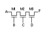
●a. In Figure 2.36 suppose we set A = B = C = D = '1', what is the value of F?
●b. What is the logic strength of the signal at F?
●c. If V DD = 5 V and V t n = 0.6 V, what would the voltage at the source and drain terminals of M1, M2, and M3 be?
●d. Will this circuit still work if V DD = 3 V?
●e. At what point does it stop working?
FIGURE 2.35
FIGURE 2.36 A pass transistor chain (Problem 2.18).
2.19 (Transistor parameters, 20 min.) Calculate the (a) electron and (b) hole mobility for the transistor parameters given in Section 2.1 if k ' n = 80 mA V 2 and k ' p = 40 mA V 2 .
Answer: (a) 0.023 m 2 V 1 s 1 .
2.20(Quantum behavior, 10 min.) The average thermal energy of an electron is approximately kT , where k = 1.38 ¥ 10 23 JK 1 is Boltzmann s constant and T is the absolute temperature in kelvin.
●a. The kinetic energy of an electron is (1/2) m v 2 , where v is due to random thermal motion, and m = 9.11 ¥ 10 31 kg is the rest mass. What is v at 300 K?
●b. The electron wavelength l = h / p , where h = 6.62 ¥ 10 34 Js is the Planck constant, and p = m v is the electron momentum. What is l at 25 C?
●c. Compare the thermal velocity with the saturation velocity.
●d. Compare the electron wavelength with the MOS channel length and with the gate-oxide thickness in a 0.25 m m process and a 0.1 m m process.
2.21(Gallium arsenide, 5 min.) The electron mobility in GaAs is about 8500 cm 2 V 1 s 1 ; the hole mobility is about 400 cm 2 V 1 s 1 . If we could make complementary n -channel and p -channel GaAs transistors (the same way that we do in a CMOS process) what would the ratio of a GaAs inverter be to equalize rise and fall times? About how much faster would you expect GaAs transistors to be than silicon for the same transistor sizes?
2.22(Margaret of Anjou, 5 min.)
●a. Why is it ones complement but two s complement?
●b. Why Queen s University, Belfast but Queens College, Cambridge?
2.23(Logic cell equations, 5 min.) Show that Eq. 2.31, 2.36, and 2.37 are correct.
2.24(Carry-lookahead equations, 10 min.)
●a. Derive the carry-lookahead equations for i = 8. Write them in the same form as Eq. 2.56.
●b. Derive the equations for the Brent Kung structure for i = 8.
2.25(OAI cells, 20 min.) Draw a circuit schematic, including transistor sizes, for
(a) an OAI321 cell, (b) an AOI321 cell. (c) Which do you think will be larger?
2.26(**Making stipple patterns) Construct a set of black-and-white, transparent, 8-by-8 stipple patterns for a CMOS process in which we draw both well layers, the active layer, poly, and both diffusion implant layers separately. Consider only the layers up to m1 (but include m1 and the contact layer). One useful tool is the Apple Macintosh Control Panel, 'General Controls,' that changes the Mac desktop pattern.
●a. (60 min.) Create a set of patterns with which you can detect any errors (for example, n -well and p -well overlap, or n -implant and p -implant overlap).
●b. (60 min.+) Using a layout of an inverter as an example, find a set of patterns that allows you to trace transistors and connections (a very qualitative goal).
●c. (Days+) Find a set of grayscale stipple patterns that allow you to produce layouts that look nice in a report (much, much harder than it sounds).
2.27(AOI and OAI cells, 10 min.). Draw the circuit schematics for an AOI22 and an OAI22 cell. Clearly label each transistor as on or off for each cell for an input vector of (A1, A2, B1, B2) = (0101).
2.28(Flip-flops and latches, 10 min.) In no more than 20 words describe the difference between a flip-flop and a latch.
2.29(**An old argument) Should setup and hold times appear under maximum, minimum, or typical in a data sheet? (From Peter Alfke.)
2.30(***Setup, 20 min.) There is no such thing as a setup and hold time, just two setup times for a '1' and for a '0'. Comment. (From Clemenz Portmann.)
2.31(Subtracter, 20 min.) Show that you can rewrite the equations for a full subtracter (Eqs. 2.65 2.66) to be the same as a full adder except that A is inverted in the borrow out equation, as follows:
DIFF = A • B • BIN |
|
SUM(A, B, BIN) , |
(2.70) |
BOUT = NOT(A) · B + NOT(A) · BIN + B · BIN |
|
MAJ(NOT(A), B, CIN) . |
(2.71) |
Explain very carefully why we need to connect BIN[0] to VSS. Show that for a subtracter implemented by inverting the B input of an adder and setting CIN[0] = '1', the true overflow for ones complement or two s complement representations is XOR(CIN[MSB], CIN[MSB 1]). Does this hold for the above subtracter?
2.32(Complex CMOS cells) Logic synthesis has completely changed the nature of combinational logic design. Synthesis tools like to see a huge selection of cells from which to choose in order to optimize speed or area.
●a. (20 min.) How many AOI nnnn cells are there, if the maximum value of n = 4?
●b. (30 min.) Consider cells of the form AOI nnnn where n can be negativeindicating a set of inputs are inverted. Thus, an AOI-22 (where the hyphen '-' indicates the following input is inverted) is a NOR(NOR(A, B), AND(C, D)), for example. How many logically different cells of the AOI xxxx family are there if x can be '-2', '-1', '1', or '2' with no more than four inputs? Remember the AOI family includes OAI, AO, and OA cells as well as just AOI. List them using an extension to the notation for a cell with mixed-sign inputs: for example, an AO(1-1)1 cell is NOT(NOR(AND(A, NOT(B)), C)). Hint: Be very careful because some cells with negative inputs are logically equivalent to others with positive inputs.
●c. (10 min.) If we include NAND and NOR cells with inverting inputs in a library, how many different cells in the NAND family are there with four or fewer inputs (the NAND family includes NOR, AND, and OR cells)?
●d. (30 min.) How many cells in the AOI and NAND families are there with four inputs or less that use fewer than eight transistors? Include cells that are logically equivalent but have different physical implementations. For example, a NAND1-1 cell, requiring six transistors, is logically equivalent to an OR1-1 cell that requires eight transistors. The OR1-1 implementation may be useful because the output inverter can easily be sized to produce an OR1-1 cell with higher drive.
●e. (**60 min.) How many cells are there with fewer than four inputs that do not fit into the AOI or NAND families? Hint: There is an inverter, a buffer, a half-adder, and the three-input majority function, for example.
●f. (***) Recommend a better, user-friendly, naming system (which is also CAD tool compatible) for combinational cells.
2.33(**Design rules, 60 min.) A typical set of deep submicron CMOS design rules is shown in Table 2.16. Design rules are often confusing and use the following buzz-words, perhaps to prevent others from understanding them.
●The end cap is the extension of poly gate beyond the active or diffusion.
●Overlap . Normally one material is completely contained within the other, overlap is then the amount of the surround.
●Extension refers to the extension of diffusion beyond the poly gate.

●Same (in a spacing rule) means the space to the same type of diffusion or implant.
●Opposite refers to the space to the opposite type of diffusion or implant.
●A dogbone is the area surrounding a contact. Often the spacing to a dogbone contact is allowed be slightly less than to an isolated line.
●Field is the area outside the active regions. The field oxide (sandwiched between the diffusion layers and the poly or m1 layers) is thicker than the gate oxide and separates transistors.
●Exact refers to contacts that are all the same size to simplify fabrication.
●A butting contact consists of two adjacent diffusions of the opposite type (connected with metal). This occurs when a well contact is placed next to a source contact.
●Fat metal . Some design rules use different spacing for metal lines that are wider than a certain amount.
●a. Draw a copy of the MOSIS rules as shown in Figure 2.11, but using the rule numbers and values in microns and l from Table 2.16.
●b. How compatible are the two sets of rules?
TABLE 2.16 ASIC design rules (Problem 2.33). Absolute values in microns are given for l = 0.2 m m.
Layer Rule 2
nwell N.1 width N.2 sp. (same)
diff D.1 width
D.2 transistor width D.3 sp. (same) D.4 sp. (opposite) D.5 p+ (nwell) to
n+ (pwell)
D.6 nwell ov. of n+
D.7 nwell sp. to p+
m m l Layer
2 10 implant
1 5
0.52.5
0.63
0.6 3
0.8 4
2.4 12
0.6 3
0.6 3 contact
Rule |
m m |
|
I.1 width |
0.6 |
|
I.2 sp. (same) |
0.6 |
|
I.3 sp. to diff |
0.55 |
|
(same) |
||
|
||
I.4 sp. to |
0 |
|
butting diff |
||
|
||
I.4 ov. of diff |
0.25 |
|
I.5 sp. to poly |
0.5 |
|
on active |
|
|
I.6 sp. |
0.3 |
|
(opposite) |
||
|
||
I.7 sp. to |
|
|
butting |
0 |
|
implant |
|
C.1 size |
0.4 |
|
(exact) |
||
|
l
3
3
2.75
0
1.25
2.5
1.5
0
2
D.8 |
|
|
|
|
extension |
0.6 |
3 |
|
|
over gate |
|
|
|
|
D.9 nwell |
1.2 |
6 |
|
|
ov. of p+ |
|
|||
|
|
|
||
D.10 nwell |
1.2 |
6 |
|
|
sp. to n+ |
|
|
|
|
poly P.1 width |
0.4 |
2 |
|
|
P.2 gate |
0.4 |
2 |
|
|
P.3 sp. |
|
|
|
|
(over |
0.6 |
3 |
|
|
active) |
|
|
|
|
P.4 sp. |
0.5 |
2.5 |
m1 |
|
(over field) |
||||
P.5 short |
|
|
+ |
|
sp. |
0.45 |
2.25 |
||
(dogbone) |
|
|
m2/m3 |
|
|
|
|
||
P.6 end cap |
0.45 |
2.25 |
|
|
P.7 sp. to |
0.2 |
1 |
v1 |
|
diffusion |
||||
|
|
|
+v2/v3
C.2 sp. |
0.6 |
3 |
|
C.3 poly ov. |
0.3 |
1.5 |
|
C.4 diff ov. (2 |
0.25/0.35 |
1.25/1.75 |
|
sides/others) |
|
|
|
C.5 metal ov. |
0.25 |
1.25 |
|
C.6 sp. to poly 0.3 |
1.5 |
||
C.7 poly |
0.5 |
2.5 |
|
contact to diff |
|||
Mn.1 width |
0.6/0.7/1.0 3/3.5/4 |
||
Mn.2 sp. (fat |
0.6/0.7/1.0 3/3.5/4 |
||
> 25 l is 5 l ) |
|||
|
|
||
Mn.3 sp. |
0.5 |
2.5 |
|
(dogbone) |
|||
|
|
||
Vn.1 size |
0.4 |
2 |
|
(exact) |
|||
|
|
||
Vn.2 sp. |
0.8 |
4 |
|
Vn.3 metal |
0.25 |
1.25 |
|
ov. |
|||
|
|
||
2.34(ESD, 10 min.)
●a. Explain carefully why a CMOS device can withstand a 2000 V ESD event when the gate breakdown voltage is only 5 10 V, but that shorting a device pin to a 10 V supply can destroy it.
●b. Explain why an electric shock from a 240 VAC supply can kill you, but an 3000 VDC shock from a static charge (walking across a nylon carpet and touching a metal doorknob) only gives you a surprise.
2.35(*Stacks in CMOS cells, 60 min.)
●a. Given a CMOS cell of the form AOI ijk or OAI ijk ( i, j, k > 0) derive an equation for the height (the number of transistors in series) and the width (the number of transistor in parallel) of the n -channel and p -channel stacks.
●b. Suppose we increase the number of indices to four, i.e. AOI ijkl . How do your equations change?
●c. If the stack height cannot be greater than three, which three-index AOI ijk and OAI ijk cells are illegal? Often limiting the stack height to three or four is a design rule for radiation-hard libraries useful for satellites.
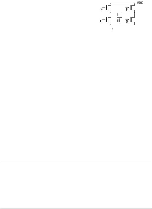
2.36 (Duals, 20 min.) Draw the n -channel stack (including device sizes, assuming a ratio of 2) that complements the p -channel stack shown in Figure 2.37.
FIGURE 2.37 A p -channel stack using a bridge device, E (Problem 2.36).
2.37(***FPGA conditional-sum adder, days+) A Xilinx application-note (M. Klein, Conditional sum adder adds 16 bits in 33 ns, Xilinx Application Brief, Xilinx data book, 1992, p. 6-26) describes a 16-bit conditional-sum adder using 41 CLBs in three stages of addition; see also [Sklansky, 1960]. A Xilinx XC3000 or XC4000 CLB can perform any logic function of five variables, or two functions of (the same) four variables. Can you find a solution with fewer CLBs in three stages? Hint: R. P. Halverson of the University of Hawaii produced a solution with 36 CLBs.
2.38(Encoding, 10 min.) Booth s algorithm was suggested by a shortcut used by operators of decimal calculating machines that required turning a handle. To multiply 5 by 23 you set the levers to 5 and turned the handle three times, change gears and turn twice more.
●a. What is the equivalent of 1 423 4 3 ?
●b. How many turns do we save using the shortcut?
2.39(CSD, 20 min.)
●a. Show how to convert 1010111 (decimal 87) to the CSD vector 10 1 0 1 00 1 .
●b. Convert 1000101 to the CSD vector.
●c. How do you know that 1 1 10011 1 (decimal 101) is not the CSD vector representation of 1100101 (decimal 101)?
1.Depths of layers are in angstroms (negative values are etch depths). For abbreviations used, see Problem 2.7.
2.sp. = space; ov. = overlap; same = same diffusion or implant type; opposite = opposite implant or diffusion type;
diff = p+ or n+; p+ = p+ diffusion; n+ = n+ diffusion; implant = p+ or n+ implant select.
2.11 Bibliography
The topics of this chapter are covered in more detail in Weste and Eshraghian [1993]. The simulator SPICE was developed at UC Berkeley and now has many commercial derivatives including Meta Software s HSPICE and Microsim s PSpice. Mead [1989] gives a description of MOS transistor operation in the subthreshold region of operation. Muller and Kamins provide an introduction to device physics [1977 and 1986]. Sze [1988]; Chang and Sze [1996]; and Campbell [1996] cover process technology in detail at an advanced level. Rabaey [1996] describes full-custom CMOS datapath circuit design, Chandrakasan and Brodersen [1995] describe low-power datapath design. Books by Brodersen [1992] and Gajski [1988] cover silicon compilers. Mukherjee [1986] covers CMOS process and fabrication issues at an introductory level. Texts on analog ASIC design include Haskard and May [1988], and Trontelj [1989]. J. Y. Chen [1990] and Uyemura [1992] provide an analysis of combinational and sequential logic design. The book by Diaz [1995] contains hard to find material on I/O cell design for ESD protection. The patent literature is the only source for often proprietary high-speed and quiet I/O design. Wakerly [1994] and Katz [1994] are basic references for CMOS logic design (including sequential logic and binary arithmetic) though they emphasize PLDs rather than ASICs. Advanced material on computer arithmetic can be found in books by Hwang [1979]; Waser and Flynn [1982]; Cavanagh [1984]; and C. H. Chen [1992].
A large number of papers on digital arithmetic were published in the 1960s. In ASIC design we work at the architectural level and not at the transistor level and so this early work is useful. Many of these early papers appeared in the IRE Transactions on Computers that changed to IRE Transactions on Electronic Computers (ISSN 0367-7508, 1963 67) and then to the IEEE Transactions on Computers (ISSN 0018-9340, 1967 ). A series of important papers on multipliers appeared in Alta Frequenza (ISSN 0002-6557, 1932 89; ISSN 1120-1908, 1989 ) [Dadda, 1965; Dadda and Ferrari, 1968]. Copies of these papers may be obtained through interlibrary loans (in the United States from Texas A&M library, for example). The two volumes by Swartzlander [1990] contain reprints of some of these articles. Ranganathan [1993] contains reprints of more recent articles. Papers on CMOS logic and arithmetic may be found in the reports of the following conferences: Proceedings of the Symposium on Computer Arithmetic (QA76.9.C62.S95a, ISSN 1063-6889), IEEE International Conference on Computer Design (TK7888.4.I35a, ISSN 1063-6404), and the IEEE International Solid-State Circuits Conference (TK7870.I58; ISSN 0074-8587, 1960-68; ISSN 0193-6530, 1969 ). Papers on arithmetic and algorithms that are more theoretical

in nature can be found in the Journal of the Association of Computing Machinery
. Online ACM journal articles can be found at http://www.acm.org .