


16.1 Floorplanning
Figure 16.3 shows that both interconnect delay and gate delay decrease as we scale down feature sizes but at different rates. This is because interconnect capacitance tends to a limit of about 2 pFcm 1 for a minimum-width wire while gate delay continues to decrease (see Section 17.4, Circuit Extraction and DRC ) Floorplanning allows us to predict this interconnect delay by estimating interconnect length.
FIGURE 16.3 Interconnect and gate delays. As feature sizes decrease, both average interconnect delay and average gate delay decreasebut at different rates. This is because interconnect capacitance tends to a limit that is independent of scaling. Interconnect delay now dominates gate delay.
16.1.1 Floorplanning Goals and
Objectives
The input to a floorplanning tool is a hierarchical netlist that describes the interconnection of the blocks (RAM, ROM, ALU, cache controller, and so on); the logic cells (NAND, NOR, D flip-flop, and so on) within the blocks; and the logic cell connectors (the terms terminals , pins , or ports mean the same thing as connectors ). The netlist is a logical description of the ASIC; the floorplan is a physical description of an ASIC. Floorplanning is thus a mapping between the logical description (the netlist) and the physical description (the floorplan).
The goals of floorplanning are to:
●arrange the blocks on a chip,
●decide the location of the I/O pads,
●decide the location and number of the power pads,
●decide the type of power distribution, and
●decide the location and type of clock distribution.
The objectives of floorplanning are to minimize the chip area and minimize delay. Measuring area is straightforward, but measuring delay is more difficult and we shall explore this next.
16.1.2 Measurement of Delay in
Floorplanning
Throughout the ASIC design process we need to predict the performance of the final layout. In floorplanning we wish to predict the interconnect delay before we complete any routing. Imagine trying to predict how long it takes to get from Russia to China without knowing where in Russia we are or where our destination is in China. Actually it is worse, because in floorplanning we may move Russia or China.
To predict delay we need to know the parasitics associated with interconnect: the interconnect capacitance ( wiring capacitance or routing capacitance ) as well as the interconnect resistance. At the floorplanning stage we know only the fanout ( FO ) of a net (the number of gates driven by a net) and the size of the block that the net belongs to. We cannot predict the resistance of the various pieces of the interconnect path since we do not yet know the shape of the interconnect for a net. However, we can estimate the total length of the interconnect and thus estimate the total capacitance. We estimate interconnect length by collecting statistics from previously routed chips and analyzing the results. From these statistics we create tables that predict the interconnect capacitance as a function of net fanout and block size. A floorplanning tool can then use these predicted-capacitance tables (also known as interconnect-load tables or wire-load tables ). Figure 16.4 shows how we derive and use wire-load tables and illustrates the following facts:

FIGURE 16.4 Predicted capacitance. (a) Interconnect lengths as a function of fanout (FO) and circuit-block size. (b) Wire-load table. There is only one capacitance value for each fanout (typically the average value). (c) The wire-load table predicts the capacitance and delay of a net (with a considerable error). Net A and net B both have a fanout of 1, both have the same predicted net delay, but net B in fact has a much greater delay than net A in the actual layout (of course we shall not know what the actual layout is until much later in the design process).
●Typically between 60 and 70 percent of nets have a FO = 1.
●The distribution for a FO = 1 has a very long tail, stretching to interconnects that run from corner to corner of the chip.
●The distribution for a FO = 1 often has two peaks, corresponding to a distribution for close neighbors in subgroups within a block, superimposed on a distribution corresponding to routing between subgroups.
●We often see a twin-peaked distribution at the chip level also, corresponding to separate distributions for interblock routing (inside blocks) and intrablock routing (between blocks).
●The distributions for FO > 1 are more symmetrical and flatter than for FO = 1.
●The wire-load tables can only contain one number, for example the average net capacitance, for any one distribution. Many tools take a worst-case approach and use the 80or 90-percentile point instead of the average.

Thus a tool may use a predicted capacitance for which we know 90 percent of the nets will have less than the estimated capacitance.
●We need to repeat the statistical analysis for blocks with different sizes. For example, a net with a FO = 1 in a 25 k-gate block will have a different (larger) average length than if the net were in a 5 k-gate block.
●The statistics depend on the shape (aspect ratio) of the block (usually the statistics are only calculated for square blocks).
●The statistics will also depend on the type of netlist. For example, the distributions will be different for a netlist generated by setting a constraint for minimum logic delay during synthesis which tends to generate large numbers of two-input NAND gates than for netlists generated using minimum-area constraints.
There are no standards for the wire-load tables themselves, but there are some standards for their use and for presenting the extracted loads (see Section 16.4 ). Wire-load tables often present loads in terms of a standard load that is usually the input capacitance of a two-input NAND gate with a 1X (default) drive strength.
TABLE 16.1 A wire-load table showing average interconnect lengths (mm). 1
|
|
|
Fanout |
|
Array (available gates) |
Chip size (mm) |
1 |
2 |
4 |
3 k |
3.45 |
0.56 |
0.85 |
1.46 |
11 k |
5.11 |
0.84 |
1.34 |
2.25 |
105 k |
12.50 |
1.75 |
2.70 |
4.92 |
Table 16.1 shows the estimated metal interconnect lengths, as a function of die size and fanout, for a series of three-level metal gate arrays. In this case the interconnect capacitance is about 2 pFcm 1 , a typical figure.
Figure 16.5 shows that, because we do not decrease chip size as we scale down feature size, the worst-case interconnect delay increases. One way to measure the worst-case delay uses an interconnect that completely crosses the chip, a coast-to-coast interconnect . In certain cases the worst-case delay of a 0.25 m m process may be worse than a 0.35 m m process, for example.
FIGURE 16.5 Worst-case interconnect delay. As we scale circuits, but avoid scaling the chip size, the worst-case interconnect delay increases.
16.1.3 Floorplanning Tools
Figure 16.6 (a) shows an initial random floorplan generated by a floorplanning tool. Two of the blocks, A and C in this example, are standard-cell areas (the chip shown in Figure 16.1 is one large standard-cell area). These are flexible blocks (or variable blocks ) because, although their total area is fixed, their shape (aspect ratio) and connector locations may be adjusted during the placement step. The dimensions and connector locations of the other fixed blocks (perhaps RAM, ROM, compiled cells, or megacells) can only be modified when they are created. We may force logic cells to be in selected flexible blocks by seeding . We choose seed cells by name. For example, ram_control* would select all logic cells whose names started with ram_control to be placed in one flexible block. The special symbol, usually ' * ', is a wildcard symbol . Seeding may be hard or soft. A hard seed is fixed and not allowed to move during the remaining floorplanning and placement steps. A soft seed is an initial suggestion only and can be altered if necessary by the floorplanner. We may also use seed connectors within flexible blocks forcing certain nets to appear in a specified order, or location at the boundary of a flexible block.
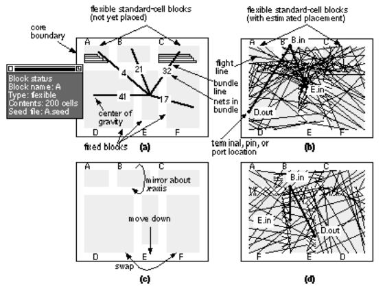
FIGURE 16.6 Floorplanning a cell-based ASIC. (a) Initial floorplan generated by the floorplanning tool. Two of the blocks are flexible (A and C) and contain rows of standard cells (unplaced). A pop-up window shows the status of block A. (b) An estimated placement for flexible blocks A and C. The connector positions are known and a rat s nest display shows the heavy congestion below block B. (c) Moving blocks to improve the floorplan. (d) The updated display shows the reduced congestion after the changes.
The floorplanner can complete an estimated placement to determine the positions of connectors at the boundaries of the flexible blocks. Figure 16.6 (b) illustrates a rat's nest display of the connections between blocks. Connections are shown as bundles between the centers of blocks or as flight lines between connectors. Figure 16.6 (c) and (d) show how we can move the blocks in a floorplanning tool to minimize routing congestion .
We need to control the aspect ratio of our floorplan because we have to fit our chip into the die cavity (a fixed-size hole, usually square) inside a package. Figure 16.7 (a) (c) show how we can rearrange our chip to achieve a square aspect ratio. Figure 16.7 (c) also shows a congestion map , another form of routability display. There is no standard measure of routability. Generally the interconnect channels , (or wiring channels I shall call them channels from now on) have a certain channel capacity ; that is, they can handle only a fixed number of interconnects. One measure of congestion is the difference between the number of interconnects that we actually need, called the channel density , and the channel capacity. Another measure, shown in Figure 16.7 (c), uses the ratio of

channel density to the channel capacity. With practice, we can create a good initial placement by floorplanning and a pictorial display. This is one area where the human ability to recognize patterns and spatial relations is currently superior to a computer program s ability.
FIGURE 16.7 Congestion analysis. (a) The initial floorplan with a 2:1.5 die aspect ratio. (b) Altering the floorplan to give a 1:1 chip aspect ratio. (c) A trial floorplan with a congestion map. Blocks A and C have been placed so that we know the terminal positions in the channels. Shading indicates the ratio of channel density to the channel capacity. Dark areas show regions that cannot be routed because the channel congestion exceeds the estimated capacity.
(d) Resizing flexible blocks A and C alleviates congestion.

FIGURE 16.8 Routing a T-junction between two channels in two-level metal. The dots represent logic cell pins. (a) Routing channel A (the stem of the T) first allows us to adjust the width of channel B. (b) If we route channel B first (the top of the T), this fixes the width of channel A. We have to route the stem of a T-junction before we route the top.
16.1.4 Channel Definition
During the floorplanning step we assign the areas between blocks that are to be used for interconnect. This process is known as channel definition or channel allocation . Figure 16.8 shows a T-shaped junction between two rectangular channels and illustrates why we must route the stem (vertical) of the T before the bar. The general problem of choosing the order of rectangular channels to route is channel ordering .
FIGURE 16.9 Defining the channel routing order for a slicing floorplan using a slicing tree. (a) Make a cut all the way across the chip between circuit blocks. Continue slicing until each piece contains just one circuit block. Each cut divides a piece into two without cutting through a circuit block. (b) A sequence of cuts: 1, 2, 3, and 4 that successively slices the chip until only circuit blocks are left.
(c) The slicing tree corresponding to the sequence of cuts gives the order in which to route the channels: 4, 3, 2, and finally 1.
Figure 16.9 shows a floorplan of a chip containing several blocks. Suppose we cut along the block boundaries slicing the chip into two pieces ( Figure 16.9 a). Then suppose we can slice each of these pieces into two. If we can continue in this fashion until all the blocks are separated, then we have a slicing floorplan ( Figure 16.9 b). Figure 16.9 (c) shows how the sequence we use to slice the chip defines a hierarchy of the blocks. Reversing the slicing order ensures that we route the stems of all the channel T-junctions first.

FIGURE 16.10 Cyclic constraints. (a) A nonslicing floorplan with a cyclic constraint that prevents channel routing. (b) In this case it is difficult to find a slicing floorplan without increasing the chip area. (c) This floorplan may be sliced (with initial cuts 1 or 2) and has no cyclic constraints, but it is inefficient in area use and will be very difficult to route.
Figure 16.10 shows a floorplan that is not a slicing structure. We cannot cut the chip all the way across with a knife without chopping a circuit block in two. This means we cannot route any of the channels in this floorplan without routing all of the other channels first. We say there is a cyclic constraint in this floorplan. There are two solutions to this problem. One solution is to move the blocks until we obtain a slicing floorplan. The other solution is to allow the use of L -shaped, rather than rectangular, channels (or areas with fixed connectors on all sides a switch box ). We need an area-based router rather than a channel router to route L -shaped regions or switch boxes (see Section 17.2.6, Area-Routing Algorithms ).
Figure 16.11 (a) displays the floorplan of the ASIC shown in Figure 16.7 . We can remove the cyclic constraint by moving the blocks again, but this increases the chip size. Figure 16.11 (b) shows an alternative solution. We merge the flexible standard cell areas A and C. We can do this by selective flattening of the netlist. Sometimes flattening can reduce the routing area because routing between blocks is usually less efficient than routing inside the row-based blocks.
Figure 16.11 (b) shows the channel definition and routing order for our chip.
FIGURE 16.11 Channel definition and ordering. (a) We can eliminate the cyclic constraint by merging the blocks A and C. (b) A slicing structure.

16.1.5 I/O and Power Planning
Every chip communicates with the outside world. Signals flow onto and off the chip and we need to supply power. We need to consider the I/O and power constraints early in the floorplanning process. A silicon chip or die (plural die, dies, or dice) is mounted on a chip carrier inside a chip package . Connections are made by bonding the chip pads to fingers on a metal lead frame that is part of the package. The metal lead-frame fingers connect to the package pins . A die consists of a logic core inside a pad ring . Figure 16.12 (a) shows a pad-limited die and Figure 16.12 (b) shows a core-limited die . On a pad-limited die we use tall, thin pad-limited pads , which maximize the number of pads we can fit around the outside of the chip. On a core-limited die we use short, wide core-limited pads . Figure 16.12 (c) shows how we can use both types of pad to change the aspect ratio of a die to be different from that of the core.
FIGURE 16.12 Pad-limited and core-limited die. (a) A pad-limited die. The number of pads determines the die size. (b) A core-limited die: The core logic determines the die size. (c) Using both pad-limited pads and core-limited pads for a square die.
Special power pads are used for the positive supply, or VDD, power buses (or power rails ) and the ground or negative supply, VSS or GND. Usually one set of VDD/VSS pads supplies one power ring that runs around the pad ring and supplies power to the I/O pads only. Another set of VDD/VSS pads connects to a second power ring that supplies the logic core. We sometimes call the I/O power dirty power since it has to supply large transient currents to the output transistors. We keep dirty power separate to avoid injecting noise into the internal-logic power (the clean power ). I/O pads also contain special circuits to protect against electrostatic discharge ( ESD ). These circuits can withstand very short high-voltage (several kilovolt) pulses that can be generated during human or machine handling.
Depending on the type of package and how the foundry attaches the silicon die to
the chip cavity in the chip carrier, there may be an electrical connection between the chip carrier and the die substrate. Usually the die is cemented in the chip cavity with a conductive epoxy, making an electrical connection between substrate and the package cavity in the chip carrier. If we make an electrical connection between the substrate and a chip pad, or to a package pin, it must be to VDD ( n -type substrate) or VSS ( p -type substrate). This substrate connection (for the whole chip) employs a down bond (or drop bond) to the carrier. We have several options:
●We can dedicate one (or more) chip pad(s) to down bond to the chip carrier.
●We can make a connection from a chip pad to the lead frame and down bond from the chip pad to the chip carrier.
●We can make a connection from a chip pad to the lead frame and down bond from the lead frame.
●We can down bond from the lead frame without using a chip pad.
●We can leave the substrate and/or chip carrier unconnected.
Depending on the package design, the type and positioning of down bonds may be fixed. This means we need to fix the position of the chip pad for down bonding using a pad seed .
A double bond connects two pads to one chip-carrier finger and one package pin. We can do this to save package pins or reduce the series inductance of bond wires (typically a few nanohenries) by parallel connection of the pads. A multiple-signal pad or pad group is a set of pads. For example, an oscillator pad usually comprises a set of two adjacent pads that we connect to an external crystal. The oscillator circuit and the two signal pads form a single logic cell. Another common example is a clock pad . Some foundries allow a special form of corner pad (normal pads are edge pads ) that squeezes two pads into the area at the corners of a chip using a special two-pad corner cell , to help meet bond-wire angle design rules (see also Figure 16.13 b and c).
To reduce the series resistive and inductive impedance of power supply networks, it is normal to use multiple VDD and VSS pads. This is particularly important with the simultaneously switching outputs ( SSOs ) that occur when driving buses off-chip [ Wada, Eino, and Anami, 1990]. The output pads can easily consume most of the power on a CMOS ASIC, because the load on a pad (usually tens of picofarads) is much larger than typical on-chip capacitive loads. Depending on the technology it may be necessary to provide dedicated VDD and VSS pads for every few SSOs. Design rules set how many SSOs can be used per VDD/VSS pad pair. These dedicated VDD/VSS pads must follow groups of output pads as they are seeded or planned on the floorplan. With some chip packages this can become difficult because design rules limit the location of package pins that may be used for supplies (due to the differing series inductance of each pin).
Using a pad mapping we translate the logical pad in a netlist to a physical pad
from a pad library . We might control pad seeding and mapping in the floorplanner. The handling of I/O pads can become quite complex; there are several nonobvious factors that must be considered when generating a pad ring:
●Ideally we would only need to design library pad cells for one orientation. For example, an edge pad for the south side of the chip, and a corner pad for the southeast corner. We could then generate other orientations by rotation and flipping (mirroring). Some ASIC vendors will not allow rotation or mirroring of logic cells in the mask file. To avoid these problems we may need to have separate horizontal, vertical, left-handed, and right-handed pad cells in the library with appropriate logical to physical pad mappings.
●If we mix pad-limited and core-limited edge pads in the same pad ring, this complicates the design of corner pads. Usually the two types of edge pad cannot abut. In this case a corner pad also becomes a pad-format changer , or hybrid corner pad .
●In single-supply chips we have one VDD net and one VSS net, both global power nets . It is also possible to use mixed power supplies (for example, 3.3 V and 5 V) or multiple power supplies ( digital VDD, analog VDD).
Figure 16.13 (a) and (b) are magnified views of the southeast corner of our example chip and show the different types of I/O cells. Figure 16.13 (c) shows a stagger-bond arrangement using two rows of I/O pads. In this case the design rules for bond wires (the spacing and the angle at which the bond wires leave the pads) become very important.

FIGURE 16.13 Bonding pads. (a) This chip uses both pad-limited and core-limited pads. (b) A hybrid corner pad. (c) A chip with stagger-bonded pads.
(d) An area-bump bonded chip (or flip-chip). The chip is turned upside down and solder bumps connect the pads to the lead frame.
Figure 16.13 (d) shows an area-bump bonding arrangement (also known as flip-chip, solder-bump or C4, terms coined by IBM who developed this technology [ Masleid, 1991]) used, for example, with ball-grid array ( BGA ) packages. Even though the bonding pads are located in the center of the chip, the I/O circuits are still often located at the edges of the chip because of difficulties in power supply distribution and integrating I/O circuits together with logic in the center of the die.
In an MGA the pad spacing and I/O-cell spacing is fixed each pad occupies a fixed pad slot (or pad site ). This means that the properties of the pad I/O are also fixed but, if we need to, we can parallel adjacent output cells to increase the drive. To increase flexibility further the I/O cells can use a separation, the I/O-cell pitch , that is smaller than the pad pitch . For example, three 4 mA driver cells can occupy two pad slots. Then we can use two 4 mA output cells in parallel to drive one pad, forming an 8 mA output pad as shown in Figure 16.14 . This arrangement also means the I/O pad cells can be changed without changing the

base array. This is useful as bonding techniques improve and the pads can be moved closer together.
FIGURE 16.14 Gate-array I/O pads. (a) Cell-based ASICs may contain pad cells of different sizes and widths. (b) A corner of a gate-array base. (c) A gate-array base with different I/O cell and pad pitches.
FIGURE 16.15 Power distribution. (a) Power distributed using m1 for VSS and m2 for VDD. This helps minimize the number of vias and layer crossings needed but causes problems in the routing channels. (b) In this floorplan m1 is run parallel to the longest side of all channels, the channel spine. This can make automatic routing easier but may increase the number of vias and layer crossings. (c) An expanded view of part of a channel (interconnect is shown as lines). If power runs on different layers along the spine of a channel, this forces signals to change layers. (d) A closeup of VDD and VSS buses as they cross. Changing layers requires a large number of via contacts to reduce resistance.
Figure 16.15 shows two possible power distribution schemes. The long direction of a rectangular channel is the channel spine . Some automatic routers may require that metal lines parallel to a channel spine use a preferred layer (either m1, m2, or m3). Alternatively we say that a particular metal layer runs in a preferred direction . Since we can have both horizontal and vertical channels, we may have the situation shown in Figure 16.15 , where we have to decide whether to use a preferred layer or the preferred direction for some channels. This may or may not be handled automatically by the routing software.
16.1.6 Clock Planning
Figure 16.16 (a) shows a clock spine (not to be confused with a channel spine) routing scheme with all clock pins driven directly from the clock driver. MGAs and FPGAs often use this fish bone type of clock distribution scheme.
Figure 16.16 (b) shows a clock spine for a cell-based ASIC. Figure 16.16 (c) shows the clock-driver cell, often part of a special clock-pad cell. Figure 16.16
(d) illustrates clock skew and clock latency . Since all clocked elements are driven from one net with a clock spine, skew is caused by differing interconnect lengths and loads. If the clock-driver delay is much larger than the interconnect delays, a clock spine achieves minimum skew but with long latency.
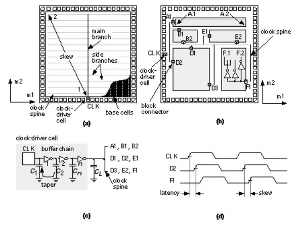
FIGURE 16.16 Clock distribution. (a) A clock spine for a gate array. (b) A clock spine for a cell-based ASIC (typical chips have thousands of clock nets).
(c) A clock spine is usually driven from one or more clock-driver cells. Delay in the driver cell is a function of the number of stages and the ratio of output to input capacitance for each stage (taper). (d) Clock latency and clock skew. We would like to minimize both latency and skew.
Clock skew represents a fraction of the clock period that we cannot use for computation. A clock skew of 500 ps with a 200 MHz clock means that we waste 500 ps of every 5 ns clock cycle, or 10 percent of performance. Latency can cause a similar loss of performance at the system level when we need to resynchronize our output signals with a master system clock.
Figure 16.16 (c) illustrates the construction of a clock-driver cell. The delay through a chain of CMOS gates is minimized when the ratio between the input capacitance C 1 and the output (load) capacitance C 2 is about 3 (exactly e ª 2.7, an exponential ratio, if we neglect the effect of parasitics). This means that the fastest way to drive a large load is to use a chain of buffers with their input and output loads chosen to maintain this ratio, or taper (we use this as a noun and a verb). This is not necessarily the smallest or lowest-power method, though.
Suppose we have an ASIC with the following specifications:
●40,000 flip-flops
●Input capacitance of the clock input to each flip-flop is 0.025 pF
●Clock frequency is 200 MHz
●V DD = 3.3 V
●Chip size is 20 mm on a side
●Clock spine consists of 200 lines across the chip
●Interconnect capacitance is 2 pFcm 1
In this case the clock-spine capacitance C L = 200 ¥ 2 cm ¥ 2 pFcm 1 = 800 pF. If we drive the clock spine with a chain of buffers with taper equal to e ª 2.7, and with a first-stage input capacitance of 0.025 pF (a reasonable value for a 0.5 m m process), we will need
800 ¥ |
10 12 |
|
log |
or 11 stages. (16.1) |
|
0.025 |
¥ 10 12 |
|
The power dissipated charging the input capacitance of the flip-flop clock is fCV 2 or
P 1 1 = (4 ¥ 10 4 ) (200 MHz) (0.025 pF) (3.3 V) 2 = 2.178 W . (16.2)
or approximately 2 W. This is only a little larger than the power dissipated driving the 800 pF clock-spine interconnect that we can calculate as follows:
P 2 1 = (200 ) (200 MHz) (20 mm) (2 pFcm 1 )(3.3 V) 2 = 1.7424 W . (16.3)
All of this power is dissipated in the clock-driver cell. The worst problem, however, is the enormous peak current in the final inverter stage. If we assume the needed rise time is 0.1 ns (with a 200 MHz clock whose period is 5 ns), the peak current would have to approach
(800 pF) (3.3 V)
I = |
ª 25 A . (16.4) |
0.1 ns |
|
Clearly such a current is not possible without extraordinary design techniques. Clock spines are used to drive loads of 100 200 pF but, as is apparent from the power dissipation problems of this example, it would be better to find a way to spread the power dissipation more evenly across the chip.
We can design a tree of clock buffers so that the taper of each stage is e • 2.7 by using a fanout of three at each node, as shown in Figure 16.17 (a) and (b). The clock tree , shown in Figure 16.17 (c), uses the same number of stages as a clock spine, but with a lower peak current for the inverter buffers. Figure 16.17 (c) illustrates that we now have another problem we need to balance the delays through the tree carefully to minimize clock skew (see Section 17.3.1, Clock Routing ).

FIGURE 16.17 A clock tree. (a) Minimum delay is achieved when the taper of successive stages is about 3. (b) Using a fanout of three at successive nodes.
(c) A clock tree for the cell-based ASIC of Figure 16.16 b. We have to balance the clock arrival times at all of the leaf nodes to minimize clock skew.
Designing a clock tree that balances the rise and fall times at the leaf nodes has the beneficial side-effect of minimizing the effect of hot-electron wearout . This problem occurs when an electron gains enough energy to become hot and jump out of the channel into the gate oxide (the problem is worse for electrons in n -channel devices because electrons are more mobile than holes). The trapped electrons change the threshold voltage of the device and this alters the delay of the buffers. As the buffer delays change with time, this introduces unpredictable skew. The problem is worst when the n -channel device is carrying maximum current with a high voltage across the channel this occurs during the rise-and fall-time transitions. Balancing the rise and fall times in each buffer means that they all wear out at the same rate, minimizing any additional skew.
A phase-locked loop ( PLL ) is an electronic flywheel that locks in frequency to an input clock signal. The input and output frequencies may differ in phase, however. This means that we can, for example, drive a clock network with a PLL in such a way that the output of the clock network is locked in phase to the incoming clock, thus eliminating the latency of the clock network . A PLL can also help to reduce random variation of the input clock frequency, known as jitter , which, since it is unpredictable, must also be discounted from the time available for computation in each clock cycle. Actel was one of the first FPGA vendors to incorporate PLLs, and Actel s online product literature explains their use in ASIC design.
1. Interconnect lengths are derived from interconnect capacitance data. Interconnect capacitance is 2 pFcm 1 .