

ATtiny261/461/861
16. Timer/Counter1
16.1Features
•10/8-Bit Accuracy
•Three Independent Output Compare Units
•Clear Timer on Compare Match (Auto Reload)
•Glitch Free, Phase and Frequency Correct Pulse Width Modulator (PWM)
•Variable PWM Period
•Independent Dead Time Generators for each PWM channels
•Five Independent Interrupt Sources (TOV1, OCF1A, OCD1B, OCF1D, FPF1)
•High Speed Asynchronous and Synchronous Clocking Modes
•Separate Prescaler Unit
16.2Overview
Timer/Counter1 is a general purpose high speed Timer/Counter module, with three independent
Output Compare Units, and with PWM support.
The Timer/Counter1 features a high resolution and a high accuracy usage with the lower prescaling opportunities. It can also support three accurate and high speed Pulse Width Modulators using clock speeds up to 64 MHz. In PWM mode Timer/Counter1 and the output compare registers serve as triple stand-alone PWMs with non-overlapping non-inverted and inverted outputs. Similarly, the high prescaling opportunities make this unit useful for lower speed functions or exact timing functions with infrequent actions. A simplified block diagram of the Timer/Counter1 is shown in Figure 16-1. For actual placement of the I/O pins, refer to ”Pinout ATtiny261/461/861” on page 2. The device-specific I/O register and bit locations are listed in the ”Register Description” on page 113.
91
2588B–AVR–11/06
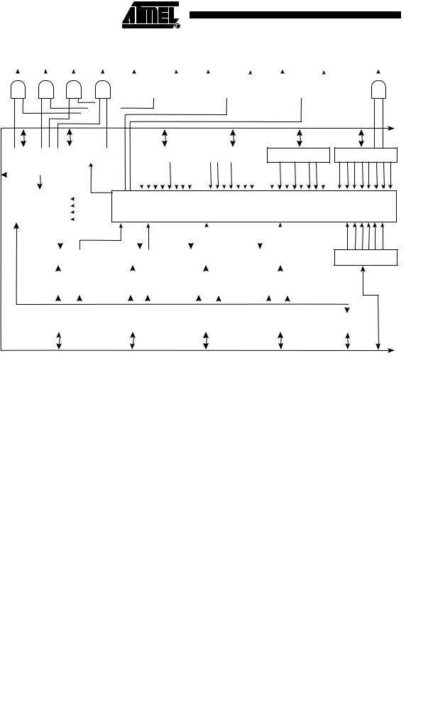
Figure 16-1. Timer/Counter1 Block Diagram
|
|
|
|
|
|
|
|
|
|
|
|
|
|
|
|
|
|
|
|
|
|
|
|
|
|
TOV1 |
OCF1A OCF1B |
OCF1D |
OC1A |
OC1A |
|
OC1B |
OC1B |
|
|
OC1D |
OC1D |
FAULT_PROTECTION |
|||||||||||||
|
|
|
|
|
|
|
|
|
|
|
|
|
|
|
|
|
|
|
|
|
|
|
|||
|
|
|
|
|
|
|
|
|
|
|
|
|
|
|
|
|
|
|
|
|
|
|
|
|
|
|
|
|
|
|
|
|
|
|
|
|
|
|
|
|
|
|
|
|
|
|
|
|
|
|
|
|
|
|
|
|
|
|
DEAD TIME GENERATOR |
|
DEAD TIME GENERATOR |
|
DEAD TIME GENERATOR |
|
|
||||||||||||
|
|
|
|
|
|
|
|
|
|
|
|
|
|
|
|
|
|
|
|
|
|
|
|
|
|
|
|
|
|
|
|
|
|
|
|
|
|
|
|
|
|
|
|
OCW1A |
|
|
|
|
|
|
|
|
|
|
|
|
|
|
|
|
|
|
|
|
|
|
|
||||
|
|
|
|
|
|
|
|
|
|
|
|
|
|
|
|
|
|
OCW1B |
|
|
|
|
|
|
|
|
|
|
|
|
|
|
|
|
|
|
|
|
|
|
|
||||
|
|
|
|
|
|
|
|
|
|
|
|
|
|
|
|
|
|
OCW1D |
|
|
|
|
|
|
|
|
|
|
|
|
|
|
|
|
|
|
|
|
|
|
|
||||
|
TOIE1 |
|
OCIE1A |
OCIE1B OCIE1D |
|
|
TOV1 |
OCF1A |
OCF1B |
|
|
OCF1D |
|
|
|
|
|
|
|
|
|
|
|
|
|
|
|
|
|
|
|
|
|
|
|
|
|
|
|
|
|
|
|||
|
|
T/C INT. MASK |
|
|
T/C INT. FLAG |
|
|
|
|
|
T/C CONTROL |
|
|
T/C CONTROL |
|
|
|
|
T/C CONTROL |
|
|
||||||||||||||||||||||||
|
REGISTER (TIMSK) |
|
|
REGISTER (TIFR) |
|
|
|
REGISTER A (TCCR1A) |
|
REGISTER B (TCCR1B) |
REGISTER C (TCCR1C) |
||||||||||||||||||||||||||||||||||
|
|
|
|
|
|
|
|
|
CLK |
|
|
|
|
|
COM1A1 |
COM1A0 |
COM1B1 |
COM1B0 |
FOC1A |
FOC1B |
PWM1A |
PWM1B |
|
|
|
PSR1 PSR1 PSR1 |
CS13 CS12 |
CS11 |
|
CS10 |
|
COM1A1 |
COM1A0 COM1B1 |
COM1B0 COM1D1 |
COM1D0 |
FOC1D |
PWM1D |
|
|||||||
|
|
|
|
|
|
|
|
|
|
|
|||||||||||||||||||||||||||||||||||
|
|
|
|
|
|
|
|
|
|
|
|
|
|
|
|
|
|
|
|
|
|
|
|
|
|
|
|
|
|
|
|
|
|
|
|
|
|
|
|
|
|||||
|
|
|
|
|
|
|
|
|
|
|
|
|
|
|
|
|
|
|
|
|
|
|
|
|
|
|
|
|
|
|
|
|
|
|
|
|
|
|
|
|
|||||
|
|
TIMER/COUNTER1 |
|
|
COUNT |
|
|
|
|
|
|
|
|
|
|
|
|
|
|
|
|
|
|
TIMER/COUNTER1 CONTROL LOGIC |
|
|
|
||||||||||||||||||
|
|
|
(TCNT1) |
|
|
CLEAR |
|
|
|
|
|
|
|
|
|
|
|
|
|
|
|
|
|
|
|
|
|
||||||||||||||||||
|
|
|
|
|
|
|
|
|
|
|
|
|
|
|
|
|
|
|
|
|
|
|
|
|
|
|
|
|
|
|
|
|
|
|
|
|
|||||||||
|
|
|
|
|
|
|
|
|
DIRECTION |
|
|
|
|
|
|
|
|
|
|
|
|
|
|
|
|
|
|
|
|
|
|
|
|
|
|
|
|
|
|
|
|
||||
|
|
|
|
|
|
|
|
|
|
|
|
|
|
|
|
|
|
|
|
|
|
|
|
|
|
|
|
|
|
|
|
|
|
|
|
|
|
|
|
|
|
|
|
|
|
|
|
|
|
|
|
|
|
|
|
|
|
|
|
|
|
|
|
|
|
|
|
|
|
|
|
|
|
|
|
|
|
|
|
|
|
|
|
|
|
|
|
|
|
|
|
|
|
|
|
|
|
|
|
|
|
|
|
|
|
|
|
|
|
|
|
|
|
|
|
|
|
|
|
|
|
|
|
|
|
|
|
|
|
|
|
|
|
|
|
|
|
|
|
|
|
|
|
|
|
|
|
|
|
|
|
|
|
|
|
|
|
|
|
|
|
|
|
|
|
|
|
|
|
|
|
|
|
|
|
|
|
|
|
|
|
|
|
|
|
|
10-BIT COMPARATOR |
|
|
10-BIT COMPARATOR |
|
|
|
|
10-BIT COMPARATOR |
|
|
|
10-BIT COMPARATOR |
|
|
|
|||||||||||||||||||||||||||
|
|
|
|
|
|
|
|
|
|
|
|
|
|
|
|
|
|
|
|
|
|
|
|
|
|
|
|
|
|
|
|
|
|
|
|
|
|
|
|
|
|
||||
|
|
|
|
|
|
|
|
|
|
|
|
|
|
|
|
|
|
|
|
|
|
|
|
|
|
|
|
|
|
|
|
|
|
|
|
|
|
|
|
|
|
|
|
|
|
|
|
|
|
|
|
|
|
|
|
|
|
|
|
|
|
|
|
|
|
|
|
|
|
|
|
|
|
|
|
|
|
|
|
|
|
|
|
|
|
|
|||||
|
|
|
10-BIT OUTPUT |
|
|
10-BIT OUTPUT |
|
|
|
|
|
10-BIT OUTPUT |
|
|
|
|
10-BIT OUTPUT |
|
|
|
|||||||||||||||||||||||||
|
|
|
COMPARE REGISTER A |
|
|
COMPARE REGISTER B |
|
|
|
COMPARE REGISTER C |
|
|
|
COMPARE REGISTER D |
|
|
|
||||||||||||||||||||||||||||
|
|
|
|
|
|
|
|
|
|
|
|
|
|
|
|
|
|
|
|
|
|
|
|
|
|
|
|
|
|
|
|
|
|
|
|
|
|
|
|
|
|
|
|
|
|
FPIE1 |
FPF1 |
T/C CONTROL
REGISTER C (TCCR1D)
FPIE1 |
FPEN1 |
FPNC1 |
FPES1 |
FPAC1 |
FPF1 |
WGM11 |
WGM10 |
|
OC1OE5 |
OC1OE4 |
OC1OE3 |
OC1OE2 |
OC1OE1 |
OC1OE0 |
|
T/C CONTROL
REGISTER D (TCCR1E)
|
|
|
|
|
|
|
|
|
|
|
|
|
|
|
|
|
|
|
|
|
|
|
|
|
|
|
|
|
|
|
|
|
|
|
|
|
|
|
|
|
|
|
|
|
|
|
|
|
|
|
|
|
|
8-BIT OUTPUT COMPARE |
|
8-BIT OUTPUT COMPARE |
|
8-BIT OUTPUT COMPARE |
|
8-BIT OUTPUT COMPARE |
|
2-BIT HIGH BYTE |
|||||||||
REGISTER A (OCR1A) |
|
REGISTER B (OCR1B) |
|
REGISTER C (OCR1C) |
|
REGISTER D (OCR1D) |
|
REGISTER (TC1H) |
|||||||||
|
|
|
|
|
|
|
|
|
|
|
|
|
|
|
|
|
|
8-BIT DATABUS
16.2.1Speed
The maximum speed of the Timer/Counter1 is 64 MHz. However, if a supply voltage below 2.7 volts is used, it is highly recommended to use the Low Speed Mode (LSM), because the Timer/Counter1 is not running fast enough on low voltage levels. In the Low Speed Mode the fast peripheral clock is scaled down to 32 MHz. For more details about the Low Speed Mode, see ”PLLCSR – PLL Control and Status Register” on page 89.
16.2.2Accuracy
The Timer/Counter1 is a 10-bit Timer/Counter module that can alternatively be used as an 8-bit Timer/Counter. The Timer/Counter1 registers are basically 8-bit registers, but on top of that there is a 2-bit High Byte Register (TC1H) that can be used as a common temporary buffer to access the two MSBs of the 10-bit Timer/Counter1 registers by the AVR CPU via the 8-bit data bus, if the 10-bit accuracy is used. Whereas, if the two MSBs of the 10-bit registers are written to zero the Timer/Counter1 is working as an 8-bit Timer/Counter. When reading the low byte of any 8-bit register the two MSBs are written to the TC1H register, and when writing the low byte of any 8-bit register the two MSBs are written from the TC1H register. Special procedures must be followed when accessing the 10-bit Timer/Counter1 values via the 8-bit data bus. These procedures are described in the section ”Accessing 10-Bit Registers” on page 110.
16.2.3Registers
The Timer/Counter (TCNT1) and Output Compare Registers (OCR1A, OCR1B, OCR1C and OCR1D) are 8-bit registers that are used as a data source to be compared with the TCNT1 contents. The OCR1A, OCR1B and OCR1D registers determine the action on the OC1A, OC1B and OC1D pins and they can also generate the compare match interrupts. The OCR1C holds the
92 ATtiny261/461/861 
2588B–AVR–11/06

 ATtiny261/461/861
Timer/Counter TOP value, i.e. the clear on compare match value. The Timer/Counter1 High
Byte Register (TC1H) is a 2-bit register that is used as a common temporary buffer to access the
MSB bits of the Timer/Counter1 registers, if the 10-bit accuracy is used.
Interrupt request (overflow TOV1, and compare matches OCF1A, OCF1B, OCF1D and fault protection FPF1) signals are visible in the Timer Interrupt Flag Register (TIFR) and Timer/Counter1 Control Register D (TCCR1D). The interrupts are individually masked with the Timer Interrupt Mask Register (TIMSK) and the FPIE1 bit in the Timer/Counter1 Control Register D (TCCR1D).
Control signals are found in the Timer/Counter Control Registers TCCR1A, TCCR1B, TCCR1C,
TCCR1D and TCCR1E.
16.2.4Synchronization
In asynchronous clocking mode the Timer/Counter1 and the prescaler allow running the CPU from any clock source while the prescaler is operating on the fast peripheral clock (PCK) having frequency of 64 MHz (or 32 MHz in Low Speed Mode). This is possible because there is a synchronization boundary between the CPU clock domain and the fast peripheral clock domain. Figure 16-2 shows Timer/Counter 1 synchronization register block diagram and describes synchronization delays in between registers. Note that all clock gating details are not shown in the figure.
The Timer/Counter1 register values go through the internal synchronization registers, which cause the input synchronization delay, before affecting the counter operation. The registers TCCR1A, TCCR1B, TCCR1C, TCCR1D, OCR1A, OCR1B, OCR1C and OCR1D can be read back right after writing the register. The read back values are delayed for the Timer/Counter1 (TCNT1) register, Timer/Counter1 High Byte Register (TC1H) and flags (OCF1A, OCF1B, OCF1D and TOV1), because of the input and output synchronization.
The system clock frequency must be lower than half of the PCK frequency, because the synchronization mechanism of the asynchronous Timer/Counter1 needs at least two edges of the PCK when the system clock is high. If the frequency of the system clock is too high, it is a risk that data or control values are lost.
93
2588B–AVR–11/06

Figure 16-2. Timer/Counter1 Synchronization Register Block Diagram.
|
|
|
|
|
8-BIT DATABUS |
|
IO-registers |
|
Input synchronization |
|
Timer/Counter1 |
Output synchronization |
|
|
|
registers |
|
|
registers |
|
OCR1A |
|
|
OCR1A_SI |
|
|
|
|
|
|
|
|
||
|
|
|
|
|
|
|
TCNT1
OCR1B |
OCR1B_SI |
TCNT1_SO |
OCR1C |
|
|
OCR1C_SI |
|
|
|
|
|
TC1H |
|
|
|
|
|
|
|
|
TC1H_SO |
|
|
|
|
|
|
|
|
|
|
|
OCR1D |
|
|
OCR1D_SI |
|
|
|
|
|
|
|
|
|
|
|
|
|
|
|
|
|
|
|
|
|
|
|
|
|
|
TCCR1A |
|
|
TCCR1A_SI |
|
|
|
|
|
|
|
|
|
|
|
|
|
|
||
|
|
|
|
|
|
|
|
|
|
|
|
|
|
|
|
|
|
|
|
TCCR1B |
|
|
TCCR1B_SI |
|
|
|
|
|
OCF1A |
|
|
|
|
|
|
|
|||
|
|
|
|
|
|
|
|
|
|
TCCR1C |
|
|
TCCR1C_SI |
|
TCNT1 |
|
|
OCF1A_SO |
|
|
|
|
|
|
|
|
|||
|
|
|
|
|
|
|
|
|
|
TCCR1D |
|
|
TCCR1D_SI |
|
|
|
|
|
|
|
|
|
|
|
|
|
|
||
|
|
|
|
|
|
|
|
|
|
TCNT1 |
|
|
TCNT1_SI |
|
|
|
|
||
|
|
|
|
|
|
|
|
|
|
TC1H |
|
|
TC1H_SI |
|
|
|
|
||
|
|
|
|
|
|
|
|
|
|
OCF1A |
|
|
OCF1A_SI |
|
|
|
|
||
|
|
|
|
|
|
|
|
|
|
OCF1B |
|
|
OCF1B_SI |
|
|
|
|
||
|
|
|
|
|
|
|
|
|
|
OCF1D |
|
|
OCF1D_SI |
|
|
|
|
||
|
|
|
|
|
OCF1B
OCF1B_SO
OCF1D
OCF1D_SO
TOV1 |
TOV1_SI |
|
|
TOV1 |
|
|
TOV1_SO |
||
PCKE |
|
|
|
|
CK |
S |
|
|
|
|
|
|
|
|
|
A |
S |
|
|
|
|
|
|
|
PCK |
|
A |
|
|
SYNC |
1/2 CK Delay |
1 CK Delay |
1 CK Delay |
1/2 CK Delay |
MODE |
|
|
|
|
ASYNC |
~1/2 CK Delay |
1 PCK Delay |
1 PCK Delay |
~1 CK Delay |
MODE |
|
|
|
|
16.2.5Definitions
Many register and bit references in this section are written in general form. A lower case “n” replaces the Timer/Counter number, in this case 0. A lower case “x” replaces the Output Compare Unit, in this case Compare Unit A, B, C or D. However, when using the register or bit defines in a program, the precise form must be used, i.e., TCNT1 for accessing Timer/Counter1 counter value and so on. The definitions in Table 16-1 are used extensively throughout the document.
Table 16-1. |
Definitions |
|
BOTTOM |
The counter reaches the BOTTOM when it becomes 0. |
|
MAX |
The counter reaches its MAXimum value when it becomes 0x3FF (decimal 1023). |
|
TOP |
The counter reaches the TOP value (stored in the OCR1C) when it becomes equal to the |
|
highest value in the count sequence. The TOP has a value 0x0FF as default after reset. |
||
|
||
|
|
94 ATtiny261/461/861 
2588B–AVR–11/06