- •Features
- •1. Pin Configurations
- •1.1 Disclaimer
- •2. Overview
- •2.1 Block Diagram
- •2.2 Pin Descriptions
- •2.2.3 AVCC
- •2.2.4 AGND
- •2.2.5 Port A (PA7..PA0)
- •2.2.6 Port B (PB7..PB0)
- •2.2.7 RESET
- •3. Resources
- •4. About Code Examples
- •5. AVR CPU Core
- •5.1 Overview
- •5.3 Status Register
- •5.4 General Purpose Register File
- •5.5 Stack Pointer
- •5.6 Instruction Execution Timing
- •5.7 Reset and Interrupt Handling
- •5.7.1 Interrupt Response Time
- •6. AVR Memories
- •6.2 SRAM Data Memory
- •6.2.1 Data Memory Access Times
- •6.3 EEPROM Data Memory
- •6.3.1 EEPROM Read/Write Access
- •6.3.2 Atomic Byte Programming
- •6.3.3 Split Byte Programming
- •6.3.4 Erase
- •6.3.5 Write
- •6.3.6 Preventing EEPROM Corruption
- •6.4 I/O Memory
- •6.4.1 General Purpose I/O Registers
- •6.5 Register Description
- •7. System Clock and Clock Options
- •7.1 Clock Systems and their Distribution
- •7.2 Clock Sources
- •7.3 Default Clock Source
- •7.4 External Clock
- •7.6 Calibrated Internal RC Oscillator
- •7.7 128 kHz Internal Oscillator
- •7.9 Crystal Oscillator
- •7.10 Clock Output Buffer
- •7.11 System Clock Prescaler
- •7.11.1 Switching Time
- •7.12 Register Description
- •8. Power Management and Sleep Modes
- •8.1 Sleep Modes
- •8.2 Idle Mode
- •8.3 ADC Noise Reduction Mode
- •8.5 Standby Mode
- •8.6 Power Reduction Register
- •8.7 Minimizing Power Consumption
- •8.7.1 Analog to Digital Converter
- •8.7.2 Analog Comparator
- •8.7.4 Internal Voltage Reference
- •8.7.5 Watchdog Timer
- •8.7.6 Port Pins
- •8.8 Register Description
- •9. System Control and Reset
- •9.0.1 Resetting the AVR
- •9.0.2 Reset Sources
- •9.0.4 External Reset
- •9.0.6 Watchdog Reset
- •9.1 Internal Voltage Reference
- •9.2 Watchdog Timer
- •9.3 Timed Sequences for Changing the Configuration of the Watchdog Timer
- •9.3.1 Safety Level 1
- •9.3.2 Safety Level 2
- •9.4 Register Description
- •10. Interrupts
- •10.1 Interrupt Vectors in ATtiny261/461/861
- •11. External Interrupts
- •11.1 Register Description
- •12. I/O Ports
- •12.1 Overview
- •12.2 Ports as General Digital I/O
- •12.2.1 Configuring the Pin
- •12.2.2 Toggling the Pin
- •12.2.3 Switching Between Input and Output
- •12.2.4 Reading the Pin Value
- •12.2.5 Digital Input Enable and Sleep Modes
- •12.2.6 Unconnected Pins
- •12.3 Alternate Port Functions
- •12.3.1 Alternate Functions of Port B
- •12.3.2 Alternate Functions of Port A
- •12.4 Register Description
- •13. Timer/Counter0 Prescaler
- •13.0.1 Prescaler Reset
- •13.0.2 External Clock Source
- •13.1 Register Description
- •14. Timer/Counter0
- •14.1 Features
- •14.2 Overview
- •14.2.1 Registers
- •14.2.2 Definitions
- •14.3 Timer/Counter Clock Sources
- •14.4 Counter Unit
- •14.5 Modes of Operation
- •14.5.1 Normal 8-bit Mode
- •14.6 Input Capture Unit
- •14.6.1 Input Capture Trigger Source
- •14.6.2 Noise Canceler
- •14.6.3 Using the Input Capture Unit
- •14.7 Output Compare Unit
- •14.7.1 Compare Match Blocking by TCNT0 Write
- •14.7.2 Using the Output Compare Unit
- •14.8 Timer/Counter Timing Diagrams
- •14.9.1 Reusing the temporary high byte register
- •14.10 Register Description
- •15. Timer/Counter1 Prescaler
- •15.0.1 Prescaler Reset
- •15.0.2 Prescaler Initialization for Asynchronous Mode
- •15.1 Register Description
- •16. Timer/Counter1
- •16.1 Features
- •16.2 Overview
- •16.2.1 Speed
- •16.2.2 Accuracy
- •16.2.3 Registers
- •16.2.4 Synchronization
- •16.2.5 Definitions
- •16.3 Counter Unit
- •16.3.1 Counter Initialization for Asynchronous Mode
- •16.4 Output Compare Unit
- •16.4.1 Force Output Compare
- •16.4.2 Compare Match Blocking by TCNT1 Write
- •16.4.3 Using the Output Compare Unit
- •16.5 Dead Time Generator
- •16.6 Compare Match Output Unit
- •16.6.1 Compare Output Mode and Waveform Generation
- •16.7 Modes of Operation
- •16.7.1 Normal Mode
- •16.7.3 Phase and Frequency Correct PWM Mode
- •16.7.4 PWM6 Mode
- •16.8 Timer/Counter Timing Diagrams
- •16.9 Fault Protection Unit
- •16.9.1 Fault Protection Trigger Source
- •16.9.2 Noise Canceler
- •16.10 Accessing 10-Bit Registers
- •16.10.1 Reusing the temporary high byte register
- •16.11 Register Description
- •17.1 Features
- •17.2 Overview
- •17.3 Functional Descriptions
- •17.3.2 SPI Master Operation Example
- •17.3.3 SPI Slave Operation Example
- •17.3.5 Start Condition Detector
- •17.4 Alternative USI Usage
- •17.4.4 Edge Triggered External Interrupt
- •17.4.5 Software Interrupt
- •17.5 Register Descriptions
- •18.1 Register Description
- •18.2 Analog Comparator Multiplexed Input
- •19.1 Features
- •19.2 Overview
- •19.3 Operation
- •19.4 Starting a Conversion
- •19.5 Prescaling and Conversion Timing
- •19.6 Changing Channel or Reference Selection
- •19.6.1 ADC Input Channels
- •19.6.2 ADC Voltage Reference
- •19.7 ADC Noise Canceler
- •19.7.1 Analog Input Circuitry
- •19.7.2 Analog Noise Canceling Techniques
- •19.7.3 ADC Accuracy Definitions
- •19.8 ADC Conversion Result
- •19.8.1 Single Ended Conversion
- •19.8.2 Unipolar Differential Conversion
- •19.8.3 Bipolar Differential Conversion
- •19.9 Temperature Measurement
- •19.10 Register Descriptin
- •19.10.3.1 ADLAR = 0
- •19.10.3.2 ADLAR = 1
- •20. debugWIRE On-chip Debug System
- •20.1 Features
- •20.2 Overview
- •20.3 Physical Interface
- •20.4 Software Break Points
- •20.5 Limitations of debugWIRE
- •20.6 Register Description
- •21. Self-Programming the Flash
- •21.0.1 Performing Page Erase by SPM
- •21.0.2 Filling the Temporary Buffer (Page Loading)
- •21.0.3 Performing a Page Write
- •21.1.1 EEPROM Write Prevents Writing to SPMCSR
- •21.1.2 Reading the Fuse and Lock Bits from Software
- •21.1.3 Preventing Flash Corruption
- •21.1.4 Programming Time for Flash when Using SPM
- •21.2 Register Description
- •22. Memory Programming
- •22.1 Program And Data Memory Lock Bits
- •22.2 Fuse Bytes
- •22.2.1 Latching of Fuses
- •22.3 Signature Bytes
- •22.4 Calibration Byte
- •22.5 Page Size
- •22.6 Parallel Programming Parameters, Pin Mapping, and Commands
- •22.6.1 Signal Names
- •22.7 Parallel Programming
- •22.7.1 Enter Programming Mode
- •22.7.2 Considerations for Efficient Programming
- •22.7.3 Chip Erase
- •22.7.4 Programming the Flash
- •22.7.5 Programming the EEPROM
- •22.7.6 Reading the Flash
- •22.7.7 Reading the EEPROM
- •22.7.8 Programming the Fuse Low Bits
- •22.7.9 Programming the Fuse High Bits
- •22.7.10 Programming the Extended Fuse Bits
- •22.7.11 Programming the Lock Bits
- •22.7.12 Reading the Fuse and Lock Bits
- •22.7.13 Reading the Signature Bytes
- •22.7.14 Reading the Calibration Byte
- •22.8 Serial Downloading
- •22.8.1 Serial Programming Algorithm
- •22.8.2 Serial Programming Instruction set
- •23. Electrical Characteristics
- •23.1 Absolute Maximum Ratings*
- •23.2 DC Characteristics
- •23.3 Speed Grades
- •23.4 Clock Characteristics
- •23.4.1 Calibrated Internal RC Oscillator Accuracy
- •23.4.2 External Clock Drive Waveforms
- •23.4.3 External Clock Drive
- •23.5 System and Reset Characteristics
- •23.7 Parallel Programming Characteristics
- •23.8 Serial Programming Characteristics
- •24. Typical Characteristics
- •24.1 Active Supply Current
- •24.2 Idle Supply Current
- •24.3 Supply Current of I/O modules
- •Example
- •24.6 Pin Driver Strength
- •24.7 Pin Threshold and Hysteresis
- •24.8 BOD Threshold and Analog Comparator Offset
- •24.9 Internal Oscillator Speed
- •24.10 Current Consumption of Peripheral Units
- •24.11 Current Consumption in Reset and Reset Pulsewidth
- •25. Register Summary
- •26. Instruction Set Summary
- •27. Ordering Information
- •27.1 ATtiny261
- •27.2 ATtiny461
- •27.3 ATtiny861
- •28. Packaging Information
- •29. Errata
- •29.1 Errata ATtiny261
- •29.2 Errata ATtiny461
- •29.3 Errata ATtiny861
- •30. Datasheet Revision History
- •Table of Contents
16.5Dead Time Generator
The Dead Time Generator is provided for the Timer/Counter1 PWM output pairs to allow driving external power control switches safely. The Dead Time Generator is a separate block that can be used to insert dead times (non-overlapping times) for the Timer/Counter1 complementary output pairs OC1x and OC1x when the PWM mode is enabled and the COM1x1:0 bits are set to “01”. The sharing of tasks is as follows: the Waveform Generator generates the Waveform Output (OCW1x) and the Dead Time Generator generates the non-overlapping PWM output pair from the Waveform Output. Three Dead Time Generators are provided, one for each PWM output. The non-overlap time is adjustable and the PWM output and it’s complementary output are adjusted separately, and independently for both PWM outputs.
Figure 16-6. Output Compare Unit, Block Diagram
top |
|
|
|
|
|
|
|
|
|
|
|
|
|
|
OCnx |
OCnx |
||||||
|
|
|
|
|
|
|
|
|
|
|
|
|
|
|||||||||
|
|
|
|
|
|
|
|
|
|
|
|
|
|
|
|
|
|
|||||
bottom |
|
|
Waveform Generator |
OCWnx |
Dead Time Generator |
|
|
|
|
|
pin |
|||||||||||
|
|
|
|
|
|
|
|
|
||||||||||||||
|
|
|
|
|
|
|
|
|
|
|
|
|||||||||||
|
|
|
|
|
|
|
|
|||||||||||||||
FOCn |
|
|
|
|
|
|
|
|
|
|
|
|
|
|
|
OCnx |
OCnx |
|||||
|
|
|
|
|
|
|
|
|
|
|
|
|
|
|
|
|
|
|
|
|
pin |
|
|
|
|
|
|
|
|
|
|
|
|
|
|
|
|
|
|
|
|
|
|||
|
|
|
|
|
|
|
|
|
|
|
|
|
|
|
|
|
|
|
|
|
|
|
|
|
|
|
|
|
|
|
|
|
|
|
|
|
|
|
|
|
|
|
|
|
|
|
|
|
|
|
|
|
|
CK OR PCK |
|
|
|
|
|
|
|
|
|
|
|
|
||
|
|
|
|
PWMnx WGM10 COMnx |
CLOCK |
DTPSn DTnH |
DTnL |
|
|
|
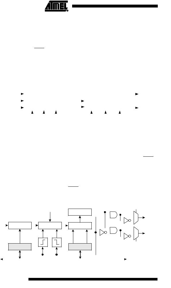
The Dead Time Generation is based on the 4-bit down counters that count the dead time, as shown in Figure 16-7. There is a dedicated prescaler in front of the Dead Time Generator that can divide the Timer/Counter1 clock (PCK or CK) by 1, 2, 4 or 8. This provides for large range of dead times that can be generated. The prescaler is controlled by two control bits DTPS11..10. The block has also a rising and falling edge detector that is used to start the dead time counting period. Depending on the edge, one of the transitions on the rising edges, OC1x or OC1x is delayed until the counter has counted to zero. The comparator is used to compare the counter with zero and stop the dead time insertion when zero has been reached. The counter is loaded with a 4-bit DT1H or DT1L value from DT1 I/O register, depending on the edge of the Waveform Output (OCW1x) when the dead time insertion is started. The Output Compare Output are delayed by one timer clock cycle at minimum from the Waveform Output when the Dead Time is adjusted to zero. The outputs OC1x and OC1x are inverted, if the PWM Inversion Mode bit PWM1X is set. This will also cause both outputs to be high during the dead time.
Figure 16-7. Dead Time Generator |
|
|
||
|
|
|
PWM1X |
|
|
|
|
COMPARATOR |
|
|
|
|
OCnx |
|
CK OR PCK |
|
|
|
|
CLOCK |
|
|
|
|
DEAD TIME |
CLOCK CONTROL |
4-BIT COUNTER |
||
PRE-SCALER |
||||
|
||||
|
|
|
OCnx |
|
DTPSn |
|
DTnH |
DTnL |
|
|
|
|
PWM1X |
|
TCCRnB REGISTER |
|
DTn I/O REGISTER |
||
OCWnx |
|
|
|
DATA BUS (8-bit)
98 ATtiny261/461/861
2588B–AVR–11/06