

CONVERSION FACTORS AND UNIT SYMBOLS
SI UNITS (ADOPTED 1960)
A new system of metric measurement, the International System of Units (abbreviated SI), is being implemented throughout the world. This system is a modernized version of the MKSA (meter, kilogram, second, ampere) system, and its details are published and controlled by an international treaty organization (The International Bureau of Weights and Measures).
SI units are divided into three classes:
Base Units |
|
length |
metery (m) |
massz |
kilogram (kg) |
time |
second (s) |
electric current |
ampere (A) |
thermodynamic temperature§ |
kelvin (K) |
amount of substance |
mole (mol) |
luminous intensity |
candela (cd) |
Supplementary Units |
|
plane angle |
radian (rad) |
solid angle |
steradian (sr) |
Derived Units and Other Acceptable Units
These units are formed by combining base units, supplementary units, and other derived units. Those derived units having special names and symbols are marked with an asterisk (*) in the list below:
Quantity |
Unit |
Symbol |
Acceptable equivalent |
*absorbed dose |
gray |
Gy |
J/kg |
acceleration |
meter per second squared |
m/s2 |
|
*activity (of ionizing radiation source) |
becquerel |
Bq |
1/s |
area |
square kilometer |
km2 |
|
|
square hectometer |
hm2 |
ha (hectare) |
|
square meter |
m2 |
|
yThe spellings ‘‘metre’’ and ‘‘litre’’ are preferred by American Society for Testing and Materials (ASTM); however, ‘‘ er’’ will be used in the Encyclopedia.
z‘‘Weight’’ is the commonly used term for ‘‘mass.’’
§Wide use is made of ‘‘Celsius temperature’’ ðtÞ defined t ¼ T T0 where T is the thermodynamic temperature, expressed in kelvins, and T0 ¼ 273:15 K by definition. A temperature interval may be expressed in degrees Celsius as well as in kelvins.
xxxi
xxxii |
CONVERSION FACTORS AND UNIT SYMBOLS |
|
|
|
|
|
|
|
Quantity |
Unit |
|
Symbol |
Acceptable |
||
|
equivalent |
|
|
|
|
|
|
|
*capacitance |
farad |
|
F |
|
C/V |
|
|
concentration (of amount of substance) |
mole per cubic meter |
mol/m3 |
|
|
||
|
*conductance |
siemens |
|
S |
|
A/V |
|
|
current density |
ampere per square meter |
A/m2 |
|
|
||
|
density, mass density |
kilogram per cubic meter |
kg/m3 |
g/L; mg/cm3 |
|||
|
* |
coulomb meter |
|
|
|
|
|
|
dipole moment (quantity) |
C m |
|
|
|
||
|
electric charge, quantity of electricity |
coulomb |
|
C |
3 |
A s |
|
|
electric charge density |
coulomb per cubic meter |
C/m |
|
|
|
|
|
electric field strength |
volt per meter |
V/m |
|
|
|
|
|
electric flux density |
coulomb per square meter |
C/m2 |
|
|
||
|
*electric potential, potential difference, |
|
|
|
|
|
|
|
electromotive force |
volt |
|
V |
|
W/A |
|
|
*electric resistance |
ohm |
|
V |
|
V/A |
|
|
*energy, work, quantity of heat |
megajoule |
|
MJ |
|
|
|
|
|
kilojoule |
|
kJ |
|
N m |
|
|
|
joule |
|
J |
|
|
|
|
|
electron volty |
y |
eVy |
|
|
|
|
|
|
hy |
|
|
||
|
energy density |
kilowatt hour |
|
kW 3 |
|
|
|
|
joule per cubic meter |
J/m |
|
|
|
||
|
*force |
kilonewton |
|
kN |
|
|
|
|
* |
newton |
|
N |
|
kg m/s2 |
|
|
frequency |
megahertz |
|
MHz |
|
|
|
|
|
hertz |
|
Hz |
|
1/s |
|
|
heat capacity, entropy |
joule per kelvin |
J/K |
K) |
|
|
|
|
heat capacity (specific), specific entropy |
|
|
|
|
|
|
|
heat transfer coefficient |
joule per kilogram kelvin |
J/(kg 2 |
|
|
||
|
watt per square meter |
W/(m K) |
|
|
|||
|
|
kelvin |
|
|
|
|
|
|
*illuminance |
lux |
|
lx |
|
lm/m2 |
|
|
*inductance |
henry |
|
H |
|
Wb/A |
|
|
linear density |
kilogram per meter |
kg/m |
|
|
||
|
luminance |
candela per square meter |
cd/m2 |
cd sr |
|
||
|
*luminous flux |
lumen |
|
lm |
|
|
|
|
magnetic field strength |
ampere per meter |
A/m |
|
|
|
|
|
* |
|
|
|
|
V s |
|
|
*magnetic flux |
weber |
|
Wb |
|
2 |
|
|
magnetic flux density |
tesla |
|
T |
|
Wb/m |
|
|
molar energy |
joule per mole |
J/mol |
|
|
||
|
molar entropy, molar heat capacity |
joule per mole kelvin |
J/(mol K) |
|
|
||
|
moment of force, torque |
newton meter |
N m |
|
|
||
|
momentum |
kilogram meter per second |
kg m/s |
|
|
||
|
permeability |
henry per meter |
H/m |
|
|
||
|
permittivity |
farad per meter |
F/m |
|
|
|
|
|
*power, heat flow rate, radiant flux |
kilowatt |
|
kW |
|
|
|
|
|
watt |
|
W |
|
J/s |
|
|
power density, heat flux density, |
|
|
|
|
|
|
|
irradiance |
watt per square meter |
W/m2 |
|
|
||
|
*pressure, stress |
megapascal |
|
MPa |
|
|
|
|
|
kilopascal |
|
kPa |
|
|
|
|
|
pascal |
|
Pa |
|
N/m2 |
|
|
sound level |
decibel |
|
dB |
|
|
|
|
specific energy |
joule per kilogram |
J/kg |
|
|
||
|
specific volume |
cubic meter per kilogram |
m3/kg |
|
|
||
|
surface tension |
newton per meter |
N/m |
|
|
||
|
thermal conductivity |
watt per meter kelvin |
W/(m K) |
|
|
||
|
velocity |
meter per second |
m/s |
|
|
|
|
|
|
kilometer per hour |
km/h |
|
|
||
|
viscosity, dynamic |
pascal second |
|
Pa s |
|
|
|
|
|
millipascal second |
mPa s |
|
|
||
yThis non-SI unit is recognized as having to be retained because of practical importance or use in specialized fields.
|
CONVERSION FACTORS AND UNIT SYMBOLS |
xxxiii |
||
Quantity |
Unit |
Symbol |
Acceptable equivalent |
|
viscosity, kinematic |
square meter per second |
m2/s |
|
|
|
square millimeter per second |
mm2/s |
|
|
|
cubic meter |
m3 |
|
|
|
cubic decimeter |
dm3 |
L(liter) |
|
|
cubic centimeter |
cm3 |
mL |
|
wave number |
1 per meter |
m 1 |
|
|
|
1 per centimeter |
cm 1 |
|
|
In addition, there are 16 prefixes used to indicate order of magnitude, as follows:
Multiplication factor |
Prefix |
Symbol |
Note |
1018 |
exa |
E |
|
1015 |
peta |
P |
|
1012 |
tera |
T |
|
109 |
giga |
G |
|
108 |
mega |
M |
|
103 |
kilo |
k |
|
102 |
hecto |
ha |
aAlthough hecto, deka, deci, and centi are |
10 |
deka |
daa |
SI prefixes, their use should be avoided |
10 1 |
deci |
da |
except for SI unit-multiples for area and |
10 2 |
centi |
ca |
volume and nontechnical use of |
10 3 |
milli |
m |
centimeter, as for body and clothing |
10 6 |
micro |
m |
measurement. |
10 9 |
nano |
n |
|
10 12 |
pico |
p |
|
10 15 |
femto |
f |
|
10 18 |
atto |
a |
|
For a complete description of SI and its use the reader is referred to ASTM E 380.
CONVERSION FACTORS TO SI UNITS
A representative list of conversion factors from non-SI to SI units is presented herewith. Factors are given to four significant figures. Exact relationships are followed by a dagger (y). A more complete list is given in ASTM E 380-76 and ANSI Z210. 1-1976.
To convert from |
To |
|
|
|
|
Multiply by |
|||
acre |
square meter (m2) |
|
4:047 |
103 |
|||||
angstrom |
meter (m) |
|
2 |
|
|
1:0 |
|
10 10y |
|
|
|
|
|
|
|||||
are |
square meter (m ) |
|
1:0 102y 11 |
||||||
astronomical unit |
meter (m) |
|
|
|
|
1:496 |
105 |
||
atmosphere |
pascal (Pa) |
|
|
|
|
1:013 |
10 |
||
bar |
pascal (Pa) |
3 |
|
|
|
1:0 105y |
|||
barrel (42 U.S. liquid gallons) |
cubic meter (m ) |
|
|
|
0.1590 |
|
|||
|
|
|
|
|
|
1:055 |
3 |
||
Btu (International Table) |
joule (J) |
|
|
|
|
103 |
|||
Btu (mean) |
joule (J) |
|
|
|
|
1:056 |
103 |
||
Bt (thermochemical) |
joule (J) |
3 |
|
|
|
1:054 |
10 |
||
bushel |
cubic meter (m ) |
|
|
|
3:524 |
|
10 2 |
||
|
|
|
|
||||||
calorie (International Table) |
joule (J) |
|
|
|
|
4.187 |
|
|
|
calorie (mean) |
joule (J) |
|
|
|
|
4.190 |
|
|
|
calorie (thermochemical) |
joule (J) |
|
|
|
|
4.184y |
|
||
centimeters of water (39.2 8F) |
pascal (Pa) |
|
|
|
2 |
98.07 |
|
|
|
centipoise |
|
|
|
1:0 |
|
10 3y |
|||
pascal second (Pa s) |
|
|
|||||||
centistokes |
square millimeter per second (mm /s) |
1.0y |
|
|
|||||
xxxiv CONVERSION FACTORS AND UNIT SYMBOLS
To convert from |
To |
|
|
|
|
Multiply by |
||||||
cfm (cubic foot per minute) |
|
3 |
|
|
|
4:72 |
|
10 4 |
||||
cubic meter per second (m3/s) |
|
|
|
|||||||||
cubic inch |
cubic meter (m3) |
|
|
|
1:639 |
10 4 |
||||||
cubic foot |
cubic meter (m3) |
|
|
|
2:832 |
10 2 |
||||||
cubic yard |
cubic meter (m ) |
|
|
|
0.7646 |
|
|
|
||||
curie |
becquerel (Bq) |
|
|
|
|
3:70 1010y |
||||||
debye |
|
|
|
|
3:336 |
|
10 30 |
|||||
coulomb-meter (C m) |
|
|
||||||||||
degree (angle) |
radian (rad) |
|
|
|
|
1:745 |
10 2 |
|||||
|
|
|
|
|
|
|||||||
denier (international) |
kilogram per meter (kg/m) |
|
1:111 |
10 7 |
||||||||
|
tex |
|
|
|
|
0.1111 |
|
|
|
|||
dram (apothecaries’) |
kilogram (kg) |
|
|
|
|
3:888 |
|
10 3 |
||||
|
|
|
|
|
|
|||||||
dram (avoirdupois) |
kilogram (kg) |
3 |
|
|
|
1:772 |
10 3 |
|||||
dram (U.S. fluid) |
cubic meter (m ) |
|
|
|
3:697 |
10 6 |
||||||
dyne |
newton(N) |
|
|
|
|
1:0 10 6y |
||||||
dyne/cm |
newton per meter (N/m) |
|
1:00 10 3y |
|||||||||
electron volt |
joule (J) |
|
|
|
|
1:602 |
10 19 |
|||||
erg |
joule (J) |
|
|
|
|
1:0 10 7y |
||||||
fathom |
meter (m) |
|
|
|
|
1.829 |
|
|
|
|
||
fluid ounce (U.S.) |
cubic meter (m3) |
|
|
|
2:957 |
10 5 |
||||||
foot |
meter (m) |
|
|
|
|
0.3048y |
|
|
||||
foot-pound force |
joule (J) |
|
|
|
|
1.356 |
|
|
|
|
||
foot-pound force |
newton meter (N m) |
|
1.356 |
|
|
|
|
|||||
foot-pound force per second |
watt(W) |
|
|
|
|
1.356 |
|
|
|
|
||
footcandle |
lux (lx) |
|
|
|
|
10.76 |
|
|
|
|
||
furlong |
meter (m) |
3 |
|
2 |
|
2:012 |
102 |
|||||
gal |
|
|
|
|
1:0 |
|
10 2y |
|||||
meter per second squared (m/s ) |
|
|
||||||||||
gallon (U.S. dry) |
cubic meter (m3) |
|
|
|
4:405 |
10 3 |
||||||
gallon (U.S. liquid) |
cubic meter (m ) |
|
|
|
3:785 |
10 3 |
||||||
gilbert |
ampere (A) |
|
|
|
|
0.7958 |
|
|
|
|||
gill (U.S.) |
cubic meter (m3) |
|
|
|
1:183 |
|
10 4 |
|||||
grad |
radian |
|
|
|
|
1:571 |
|
10 2 |
||||
|
|
|
|
|
||||||||
grain |
kilogram (kg) |
|
|
|
|
6:480 |
10 5 |
|||||
|
2 |
|
|
|
||||||||
gram force per denier |
|
|
|
|
8:826 |
10 2 |
||||||
newton per tex (N/tex) |
|
|
|
|||||||||
hectare |
square meter (m ) |
|
1:0 104y |
2 |
||||||||
horsepower (550 ft lbf/s) |
watt(W) |
|
|
|
|
7:457 |
103 |
|||||
horsepower (boiler) |
watt(W) |
|
|
|
|
9:810 |
10 |
|
||||
horsepower (electric) |
watt(W) |
|
|
|
|
7:46 102y |
||||||
hundredweight (long) |
kilogram (kg) |
|
|
|
|
50.80 |
|
|
|
|
||
hundredweight (short) |
kilogram (kg) |
|
|
|
|
45.36 |
|
|
|
3 |
||
inch |
meter (m) |
|
|
|
|
2:54 |
|
|
|
|||
|
|
|
|
|
|
10 2y |
||||||
inch of mercury (32 8F) |
pascal (Pa) |
|
|
|
|
3:386 |
102 |
|||||
inch of water (39.2 8F) |
pascal (Pa) |
|
|
|
|
2:491 |
10 |
|
||||
kilogram force |
newton (N) |
|
|
|
|
9.807 |
|
|
|
|
||
kilopond |
newton (N) |
|
|
|
|
9.807 |
|
|
|
|
||
kilopond-meter |
newton-meter (N m) |
|
9.807 |
|
|
|
|
|||||
kilopond-meter per second |
watt (W) |
|
|
|
|
9.807 |
|
|
|
|
||
kilopond-meter per min |
watt(W) |
|
|
|
|
0.1635 |
|
|
|
|||
kilowatt hour |
megajoule (MJ) |
|
|
|
3.6y |
|
|
|
|
|
||
kip |
newton (N) |
|
|
|
|
4:448 |
102 |
|||||
knot international |
meter per second (m/s) |
|
0.5144 |
|
|
|
||||||
lambert |
candela per square meter (cd/m |
2 |
3:183 |
|
3 |
|||||||
) |
102 |
|||||||||||
league (British nautical) |
meter (m) |
|
|
|
|
5:559 |
103 |
|||||
league (statute) |
meter (m) |
|
|
|
|
4:828 |
1015 |
|||||
light year |
meter (m) |
3 |
|
|
|
9:461 |
10 |
|
||||
liter (for fluids only) |
cubic meter (m ) |
|
|
|
1:0 |
|
10 3y |
|||||
maxwell |
weber (Wb) |
|
|
|
|
1:0 |
|
10 8y |
||||
|
|
|
|
|
|
|||||||
micron |
meter (m) |
|
|
|
|
1:0 10 6y |
||||||
mil |
meter (m) |
|
|
|
|
2:54 10 5y |
||||||
mile (U.S. nautical) |
meter (m) |
|
|
|
|
1:852 |
|
|
3 |
|||
|
|
|
|
|
|
103y |
||||||
mile (statute) |
meter (m) |
|
|
|
|
1:609 |
10 |
|
||||
mile per hour |
meter per second (m/s) |
|
0.4470 |
|
|
|
||||||
|
|
|
|
CONVERSION FACTORS AND UNIT SYMBOLS |
xxxv |
||||
To convert from |
To |
|
|
|
Multiply by |
||||
millibar |
pascal (Pa) |
|
|
|
1:0 102 |
|
|||
millimeter of mercury (0 8C) |
pascal (Pa) |
|
|
|
1:333 |
102y |
|||
millimeter of water (39.2 8F) |
pascal (Pa) |
|
|
|
9.807 |
|
|
|
|
minute (angular) |
radian |
|
|
|
2:909 |
10 4 |
|||
|
|
|
|
||||||
myriagram |
kilogram (kg) |
|
|
|
10 |
|
|
|
|
myriameter |
kilometer (km) |
|
|
|
10 |
|
|
|
|
oersted |
ampere per meter (A/m) |
79.58 |
|
|
|
||||
ounce (avoirdupois) |
kilogram (kg) |
|
|
|
2:835 |
10 2 |
|||
|
|
|
|
||||||
ounce (troy) |
kilogram (kg) |
3 |
|
|
3:110 |
10 2 |
|||
ounce (U.S. fluid) |
cubic meter (m ) |
|
|
2:957 |
10 5 |
||||
ounce-force |
newton (N) |
|
|
|
0.2780 |
|
|
||
peck (U.S.) |
cubic meter (m3) |
|
|
8:810 |
|
10 3 |
|||
|
|
|
|||||||
pennyweight |
kilogram (kg) |
|
|
|
1:555 |
|
10 3 |
||
pint (U.S. dry) |
cubic meter (m3) |
|
|
5:506 |
10 4 |
||||
pint (U.S. liquid) |
cubic meter (m3) |
|
|
4:732 |
|
10 4 |
|||
|
|
|
|||||||
poise (absolute viscosity) |
pascal second (Pa s) |
0.10y |
|
|
|
||||
pound (avoirdupois) |
kilogram (kg) |
|
|
|
0.4536 |
|
|
||
pound (troy) |
kilogram (kg) |
|
|
|
0.3732 |
|
|
||
poundal |
newton (N) |
|
|
|
0.1383 |
|
|
||
pound-force |
newton (N) |
|
|
|
4.448 |
|
|
|
|
pound per square inch (psi) |
pascal (Pa) |
3 |
|
|
6:895 |
103 |
|||
quart (U.S. dry) |
cubic meter (m3) |
|
|
1:101 |
10 3 |
||||
quart (U.S. liquid) |
cubic meter (m ) |
|
|
9:464 |
10 4 |
||||
quintal |
kilogram (kg) |
|
|
|
1:0 |
|
102y |
|
|
|
|
|
|
|
|||||
rad |
gray (Gy) |
|
|
|
1:0 10 2y |
||||
rod |
meter (m) |
|
|
|
5.029 |
|
|
|
|
roentgen |
coulomb per kilogram (C/kg) |
2:58 10 4 |
|||||||
second (angle) |
radian (rad) |
|
2 |
|
4:848 |
|
|
6 |
|
|
|
|
|
10 6 |
|||||
section |
square meter (m ) |
2:590 |
10 |
|
|||||
slug |
kilogram (kg) |
|
|
|
14.59 |
|
|
|
|
spherical candle power |
lumen (lm) |
|
|
|
12.57 |
|
|
|
|
square inch |
square meter (m2) |
6:452 10 4 |
|||||||
square foot |
|
|
2 |
|
9:290 |
|
|
6 |
|
square meter (m2) |
|
10 2 |
|||||||
square mile |
square meter (m2) |
2:590 |
10 |
|
|||||
square yard |
square meter (m ) |
0.8361 |
|
|
|||||
store |
cubic meter (m3) |
|
|
1:0y |
|
|
|
||
stokes (kinematic viscosity) |
square meter per second (m2/s) |
1:0 |
|
10 4y |
|||||
tex |
kilogram per meter (kg/m) |
1:0 |
|
|
|
3 |
|||
|
10 6y |
||||||||
ton (long, 2240 pounds) |
kilogram (kg) |
|
|
|
1:016 |
10 |
|
||
ton (metric) |
kilogram (kg) |
|
|
|
1:0 103y |
2 |
|||
ton (short, 2000 pounds) |
kilogram (kg) |
|
|
|
9:072 |
102 |
|||
torr |
pascal (Pa) |
|
|
|
1:333 |
10 |
|
||
unit pole |
weber (Wb) |
|
|
|
1:257 |
10 7 |
|||
yard |
meter (m) |
|
|
|
0.9144y |
|
|
||
C
A C ¼ ere0 d
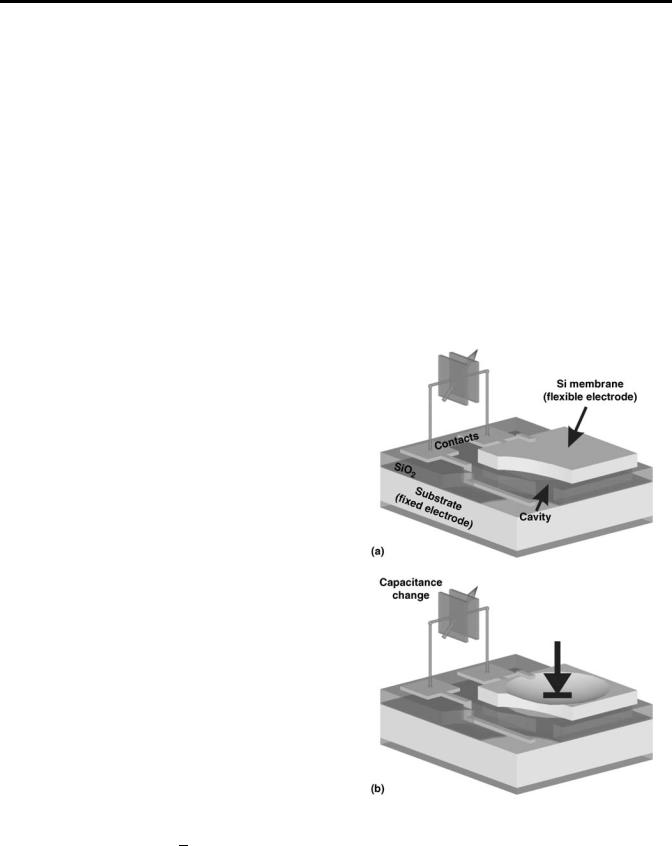
where er, e0 is the relative and vacuum permittivity constant, respectively, A is the plate surface area, and d is the plate distance.
When an applied external force acts in a way to change the distance between the two electrodes, the displacement is detected as a capacitance change. In many applications when a micromechanical structure is realized to detect a capacitance change, one of the two electrodes remains fixed and the other is flexible (Fig. 1a). The flexible electrode that is rigidly supported on its edges deflects so it does not remain parallel to the fixed electrode (Fig. 1b). In that case, the previous simple expression is modified and the capacitance is given by
C ¼ ere0 |
ð ðd |
w x; y |
(2) |
||
|
|
|
1 |
|
|
|
A |
ð Þ |
|
|
|
where w(x,y) is the displacement of the flexible electrode. Since the measured capacitance depends on the distance between the two electrodes, it can be used to calculate
Figure 1. An example of a capacitive sensor is a pressure sensor. In parts a, the thin sensor diaphragm remains parallel to the fixed
(1)electrode and in part b, the diaphragm deflects under applied pressure resulting in capacitance change.
1
2 CAPACITIVE MICROSENSORS FOR BIOMEDICAL APPLICATIONS
the value of the stimulus modifying the interelectrode spacing. Different approaches for capacitive micro devices have appeared that make use of the above principle.
One major application in the medical field for capacitive transducers is pressure measurement. First explorative research of capacitive microdevices made using silicon technology was initiated in the early 1980s (8–11). These initial studies have demonstrated that capacitive devices exhibit superior properties from their piezoresistive competitors in terms of pressure sensitivity, scalability, manufacturing simplicity, as well as process variation tolerance.
APPLICATIONS IN THE MEDICAL FIELD
The manufacturing advantages of micromachined silicon sensors have made them very attractive in the field of minimally invasive therapy. Catheters used in this field need to penetrate into small blood vessels putting stringent requirements on sensor size, which should be one-half of the size of the vessel to be accessed. In small vessels, catheters usually have a diameter of 2 mm, while the smallest catheter at the moment has a diameter of 0.36 mm (12). Miniaturization, therefore, of both sensor and packaging size drives this kind of application. Capacitive devices within the above size requirements have been demonstrated in silicon (13) and are mainly competing with fiber optic pressure sensors (14), or a free hanging strain gauge (15).
Catheters, however, are unsuitable for long-term monitoring of blood pressure. With AAA (abdominal aortas aneurism) and CHF (congestive heart failure) being the major cardiovascular diseases in our days, an implantable pressure monitoring system that would tailor treatment medication by measuring blood pressure appears very attractive. These implantable applications will require a miniature batteryless telemetric sensor able to communicate with an external handheld unit. In such applications, power consumption becomes an additional issue and capacitive devices offer a clear advantage over piezoresistive ones. These types of systems have been under investigation (16,17) and have already demonstrated good performance.
Capacitive pressure sensors have also been successfully applied in the following areas. (1) Intraocular pressure monitoring (10,18). Glaucoma is, for example, a serious disease characterized by an increased pressure in the eye that may result in blindness. In that case, a sensitive capacitive device has been developed for remote sensing of eye pressure (normally 10–20 mmHg 1.33–2.66 kPa above atmospheric pressure, but much increased in glaucoma). (2) Intracranial pressure monitoring (19), as well as for clinical assessment of prosthetic socket fit (20) and pressure distribution in artificial joints (21). Intracranial pressure monitoring is an implant used in the treatment of patients with trauma of the head as well as in neurological patients.
Although pressure is the field where capacitive sensors have been applied more extensively, there are also other applications under development in the medical field. Accelerometers, for example, are used for measuring inclination
of body segments and activity of daily living, with application in patient rehabilitation (22), but also register the kind of movements that occur in healthy persons during normal standing (23,24). Physical activity as well as energy expenditure as these can be followed by accelerometers proves to be useful information for personal status monitoring. An accelerometer design includes the fabrication of a proof mass that is displaced in proportion with acceleration. The use of capacitance to measure that displacement significantly improves sensitivity.
Recently, ultrasound imaging technology has also exploited the advantages of capacitive sensors for both transmission and detection purposes (25). Such capacitive devices can be batch fabricated to form a transducer array with array elements that can be as small as 50 mm diameter. Ultrasound devices are made of a thin flexible electrode facing a rigid electrode. For transmission purposes, the membranes are driven into vibration by the electrostatic force exerted between the two electrodes. For reception, the membrane vibration is excited by an impinging acoustic wave that is converted by the capacitive device to electrical signal. This as well as other efforts (26,27) are driven from the need to obtain in the future high resolution images within the body using three-dimensional 3D echographic probes.
Miniature capacitive transducers, known in low frequency applications as condenser microphones, are used in hearing aids and have been reported from different research groups (28,29). In their work, Rombach et al. developed a low noise capacitive microphone with higher sensitivity and broader bandwidth than those used in traditional hearing aids. This device consists of two backplates with an intermediate membrane made of a low stress silicon-rich nitride and Bþ polysilicon multilayer. Pedersen et al., on the other hand, presented an integrated capacitive microphone based on polyimide technology and realized by postprocessing on a CMOS wafer at low processing temperatures.
Capacitive sensors have also been used as humidity sensors for the diagnosis of pulmonary diseases. In this device, a chemically absorbing layer (usually a polymer) is placed between the parallel electrodes of a capacitor. Then, humidity is detected as a change in capacitance because of the dielectric constant change as water molecules are absorbed in the polymer. In a similar configuration, hydrogel has been used between the electrodes of a capacitive sensor to measure body analytes from the capacitance variation occurring due to the swelling of the polymer (30).
FABRICATION TECHNOLOGIES FOR CAPACITIVE SENSORS
Silicon is widely accepted as the material of choice for microsensor fabrication. Known for its good mechanical properties, high mechanical strength, and light weight it’s an ideal material for physical sensors (31). More importantly, the existing know-how from IC manufacturing made the use of silicon technology for transducers quite straightforward during the last decades.
This section describes the main silicon technologies that are used for the fabrication of capacitive devices. Most of
CAPACITIVE MICROSENSORS FOR BIOMEDICAL APPLICATIONS |
3 |
the capacitive devices used in medical technology, namely, pressure sensors, accelerometers, and ultrasound sensors, have been developed using two major technology platforms.
Bulk Micromachining Technologies
Bulk micromachining has historically been developed first. It consists of engineering a silicon wafer by a series of lithographic processes followed by wet or dry etching, in order to form thin membranes or other free standing structures that can move upon an external stimulation. In bulk micromachining, the micromechanical silicon structures are fabricated by selectively removing whole sections, or in some cases, all but a small part of the silicon wafer. Thus the structures fabricated in this way are made of singlecrystal silicon and have excellent mechanical properties. In bulk micromachining, processing may take place in either the front or the back side of the silicon wafer.
Wet etching of silicon is based on a chemical reaction of silicon with a base solution (KOH) in order to remove silicon material and form the intended 3D structure. Dry etching is a physicochemical process that was initially developed for the etching of thin films. During the last decade, however, this technique has also been used for the removal of thick Si material (32).
The above techniques combined with others usually used in IC manufacturing, like ion implantation, thermal processing, and thin-film (metal or silicon insulator) deposition, constitute the backbones of capacitive sensor fabrication. A detailed description of these processes is beyond the scope of this article and can be found elsewhere (33).
Apart from these processing technologies it is necessary in many applications to use other specific processes. For example, in pressure sensor fabrication it is always desirable to have a reference pressure enclosed in the sensor body. This requires a reliable technology for sealing a cavity with known pressure. For that reason, bulk micromachining techniques are combined with technologies usually referred to as bonding technologies. Two are the most established technologies in this area: anodic bonding and fusion bonding, in chronological order of their discovery and application. Anodic bonding is achieved between silicon and a glass substrate at medium temperature ( 400 8C) under the application of a direct current (dc) voltage across the two substrates (34). Prior to contact of the two substrates, their surfaces are adequately cleaned to remove any particle that can inhibit their good contact. Bulk micromachining combined with anodic bonding has been successfully used for the realization of medical capacitive pressure sensors by a couple of research groups (35,36). In the process developed at the University of Michigan, boron etch-stop techniques and silicon-glass anodic bonding is used to fabricate a capacitive pressure sensor. In this process, KOH is used to initially form a recess in the surface of a silicon wafer, followed by a deep boron diffusion to define the rim of the transducer, and a shallow diffusion defining the eventual thickness of the diaphragm. The completed silicon wafer is finally electrostatically bonded to a glass wafer. The silicon wafer is then dissolved in EDP letchant, leaving only the silicon
transducer islands bonded to the glass. In this way, a thin silicon membrane structure over a sealed cavity is fabricated that exhibits high pressure sensitivity adequate for use in blood pressure monitoring.
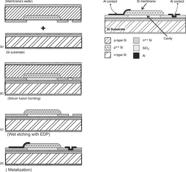
A more recently discovered technique that has been applied for sealing of a pressure reference cavity is fusion bonding. This technique does not require the application of a voltage across the bonded substrate. Instead, it includes a high temperature heat treatment. So after a thorough wafer cleaning and drying process of two silicon wafers that renders their surface hydrophilic, they are brought into contact at room temperature. The two wafers are initially drawn together at room temperature by van de Waals forces developed between the hydrogen atoms of water molecules covering their surfaces. This initial attraction is commonly known as prebonding. Prebonding follows a high temperature heat treatment that during which a hydrogen atom is removed transforming the hydrogen bonds to covalent bonds between oxygen atoms thus increasing the bonding strength (37). The temperature necessary to achieve high strength bonding is > 800 8C. A successful example of this technology together with bulk micromachining is applied for the realization of a capacitive-type pressure sensor for blood pressure monitoring developed by Goustouridis et al. (13). This simple process results in robust capacitive sensors with low parasistics (Fig. 2). It involves two silicon wafers that are silicon fusion bonded to form the final 3D structure, and a thick oxide in between in which a sealed cavity is formed. The sensor diaphragm is formed by creating a heavily boron-doped region in the cavity bottom. After bonding, the wafer stack is first mechanically ground and then etched in EDP etchant to leave the sensor diaphragm on top of the cavity thus creating the pressure sensor. The sealed cavities are then metalized and packaged. Figure 3 depicts the complete pressure sensing element as it appears after the metallization step.
Hydrophobic bonding is also applied when we need to bond two bare silicon surfaces without a SiO2 layer on the surface. This technique requires an HF final step to remove any oxide layer from the surface. In hydrophobic bonding, the water molecules necessary to complete the prebonding step are substituted from the HF molecules, while the rest of the bonding process is similar to the hydrophilic one.
More recently, plasma activated bonding (38) or other low temperature bonding (< 400 8C) using spin on glass (SOG) (39) have been applied. These techniques are more appropriate for wafer level packaging and have to be more developed in the future for use in sensor fabrication.
Recently, wafer bonding has also been used for demonstration of capacitive ultrasound devices (25), as well as of capacitive accelerometers (40).
Surface Micromachining and SOI Technologies
Surface micromachining technologies have been developed with the primary goal of cointegrating the electronic and mechanical parts on the same silicon chip. Since the active and passive layers of a surface micromachined structure are realized using the same conductive and insulating thin-film layers as in IC manufacturing, it is possible by appropriately designing the mask sequence to realize both
4 CAPACITIVE MICROSENSORS FOR BIOMEDICAL APPLICATIONS
Figure 2. Fabrication of capacitive sensors using bulk micromachining and silicon fusion bonding. Two wafers are used for this purpose. (a) Each wafer is processed independently before the bonding; (b) after the bonding process the two wafers are permanently stacked together; (c) selective wet etching releases the boron doped silicon diaphragms; (d) metallization is performed for electrical connects of the membrane and the substrate.
components in parallel by adding a few mask levels after the completion of the electronic circuit. This particular feature is behind the drive for the development of this technology.
In the case of surface micromachining, all of the processing takes place only on the surface of the front side of the silicon wafer. The micromechanical structures fabricated in this manner are made out of polycrystalline silicon deposited by low pressure chemical vapor deposition (LPCVD) techniques over a sacrificial layer. The sacrificial layer is a deposited oxide, usually phosphorsilicate glass (PSG). This layer is subsequently removed by an HF solution through narrow access channels to release the poly-
Figure 3. This figure illustrates the final capacitive pressure sensor structure (not to scale).
silicon structure (Fig. 4). Sealing of the channels is necessary and it is realized by a deposition step. With surface micromachining, it is possible to fabricate far smaller microelectromechanical devices than with bulk micromachining. Depositing processes allow for very good control over the dimensions of the deposited materials.
Surface micromachining is a very important technology with a demonstrated potential. Problems related to stiction of membrane structures on the substrate during aqueous removal of sacrificial layers have been resolved by the application of other etching and drying techniques like gas-phase etching or freeze-drying techniques using cycloexane (41). A typical process sequence developed (42) for capacitive ultrasound transducers is shown in Fig. 5.
There is continuing discussion on the advantages– disadvantages of the cointegration of sensors with electronics. Although it is considered that surface micromachining can result in a higher packing density, and consequently smaller and cheaper components, it appears that yield issues still need to be overcome until this technology can be definitively adopted in preference to hybrid fabrication technologies.
A recent variation of the two technologies employs silicon-on-insulator (SOI) technology with some unique features. The SOI technology offers the possibility of using crystalline silicon as the active part of a capacitive-type structure with more predictable mechanical behavior than the polysilicon film used in surface micromachining. In fact, the internal stresses (either compressive or tensile) developed during the growth of the polysilicon film, which evolved during subsequent thermal treatment because of change of the grain size, is a source of potential uncertainties for the behavior of these films.
Silicon-on-insulator is a mature technology and nowadays can offer crystalline silicon structures of varying thicknesses over a variety of SiO2 buried layer thicknesses. This has become possible after the discovery of wafer bonding technology, which enables the development of back-etch-silicon-on-insulator (BESOI) structures.
Thin as well as thick silicon structures allow for capacitive pressure sensors development, ultrasound capacitive sensors using rather thin membranes of some micron thickness as well as capacitive-type accelerometers, where
CAPACITIVE MICROSENSORS FOR BIOMEDICAL APPLICATIONS |
5 |
Si structures exceed some hundreds of micrometers. The introduction of deep reactive ion etching (DRIE) in silicon processing especially during the last few years, has enabled the vertical anisotropic etching of Si at the rate of several microns per minute, and the fabrication of thick proof masses on BESOI or glass structures for capacitive accelerometers (43). This accelerometer uses a silicon proof mass of 0.5 mg with 120 mm thickness formed by DRIE and measures in plane (x or y axis) acceleration. It uses a sense gap of only 2 mm between sense fingers and the electrodes (Fig. 6). As the proof mask moves under acceleration, the distance between sense fingers and fixed electrodes change, which consequently modifies the capacitance.
Finally, a different but similar approach results in capacitive-like pressure sensors based on a field effect transistor (44). In this case, the usual dielectric of a MOSFET is replaced by a vacuum cavity. The external pressure variations deflect the gate electrode, and consequently influence the capacitive coupling of the flexible membrane (gate) with the channel thus modifying the current flow in the device. Although these devices present an attractive design, there have not seen any new developments.
OPERATION ISSUES OF CAPACITIVE SENSORS
As introduced in the first paragraph a capacitive sensor is an equivalent parallel plate capacitor with clamped edges where the diaphragm deforms during the application of a deferential pressure across the two sides in the case of capacitive pressure devices.
In the normal operation mode of a capacitive pressure sensor, the diaphragm does not contact the substrate electrode. The capacitance response of a typical pressure sensor is shown in Fig. 7. The output capacitance is nonlinear because of its inverse relationship with the electrode gap d0-w (eq. 2), which is a function of pressure, P. This nonlinearity becomes more significant for large membrane
Figure 4. Typical surface micromachining process. (a) Deposition of the sacrificial layer (silicon oxide) and etch channels formation,
(b) deposition of silicon nitride ring,
(c) deposition of polysilicon film,
(d) removal of the sacrificial layer by HF in wet or vapor form, (e) sealing of the devicewithdeposited silicon oxide.
deflections. At the point when the sensor diaphragm touches the cavity bottom (Fig. 7), the behavior of the sensor changes and enters ‘‘touch mode’’ operation (45). In this operating region, linearity increases and the sensor capacitance is dominated by the area touching the cavity bottom, since the gap there is replaced from the very thin and high dielectric constant SiO2 layer of the bottom electrode.
Sensitivity of the Capacitive Sensor
Because of the nonlinearity of the response, the sensitivity of a capacitive sensor is not constant. For example, the sensitivity of the capacitive pressure sensor for blood pressure monitoring (defined as 1/C0(DC/DP) with the response shown in Fig. 7 is 1.5 fF/mmHg for the low pressure range and increases to > 18 fF/mmHg for the upper part of the measurement range (> 200 mmHg, 26.66 kPa). In the touch mode operation region, (> 300 mmHg, 39.99 kPa) the sensor has a nearly linear response with a sensitivity of 12 fF/mmHg.
Temperature variation, although not a critical issue for medical application (because of the small variation of the body temperature), can affect the accuracy of the measurements. The temperature influence on the capacitive sensor response is due to either the mismatch of thermal expansion of dissimilar materials used in the fabrication process (usually Si and SiO2), or to gas expansion in case gas is trapped in a sealed cavity of the sensor. It can of course be due to both of the above reasons. In the case of a sealed cavity, the temperature influence, because of the expansion of the gas trapped inside the cavity, can be eliminated if the cavity is sealed in vacuum. On the other hand, the effect of the different thermal expansions of the materials used is always a problem that requires appropriate design in order to reduce or even eliminate the effect. In the cases of capacitive devices fabricated with surface micromachining,

6 CAPACITIVE MICROSENSORS FOR BIOMEDICAL APPLICATIONS
Capacitance change (pF)
6
5
4
Touching pressure
3
2
1 Normal mode
0 |
Touch mode |
|
Figure 5. Surface micromachining process sequence for the fabrication of capacitive ultrasonic transducers as taken from X. Jin et al. (42).
0 |
100 |
200 |
300 |
400 |
500 |
600 |
Pressure (mmHg)
Figure 7. Typical response of a capacitive pressure sensor with 325 mm OD circular diaphragm. The diaphragm touches the cavity bottom at 300 mmHg ( 40 kPa). A pressure sensor must be designed to operate either for lower values than 300 mmHg or for higher pressure values. Otherwise an hysteresis phenomenon can be observed.
or by using anodic bonding of silicon with a glass substrate, the influence of temperature becomes more complicated.
Figure 8 shows the influence of temperature on the response of a capacitive pressure sensor, not sealed in a vacuum. The variation of the distance between the curves with temperature represents the temperature coefficient of the pressure sensitivity (TCS) while the slope of the lower curve is the temperature coefficient of zero pressure offset (TCO). The TCS is defined as DS/SDT, where S is the pressure sensitivity defined as DC/C0DP and TCO is
defined as DC/C0DT.
This simple configuration of a parallel plate capacitor is used mainly in pressure sensors and ultrasound imaging devices. Accelerometers are usually designed with combshaped electrodes that result in increased linearity and sensitivity (40,43).
|
8,0 |
|
|
|
32 °C |
|
|
|
|
|
|
|
|
|
|
|
37 °C |
(pF) |
7,5 |
|
|
|
42 °C |
|
|
|
|
47 °C |
|
Capacitance |
|
|
|
|
|
7,0 |
|
|
|
|
|
6,5 |
|
|
|
|
|
|
6,0 |
|
|
|
|
|
0 |
100 |
200 |
300 |
400 |
Pressure (mmHg)
Figure 6. Comb-shaped accelerometer structure fabricated using a combination of processes like bonding silicon with glass substrate and Deep Reactive Ion Etching (43).
Figure 8. Temperature variation of a capacitive pressure sensor in the range 0–400 mmHg ( 53.3 kPa). The effect is due mainly to trapped gas expansion inside the cavity.
CAPACITIVE MICROSENSORS FOR BIOMEDICAL APPLICATIONS |
7 |
CAPACITIVE SENSOR ELECTRONIC INTERFACES
Although capacitive sensors offer advantages with respect to high sensitivity and low power operation, they also present difficulties in the design of electronic interfaces to convert capacitance changes into electrical signals. Parasitic capacitances often dominate system performance by reducing sensitivity and increasing nonlinearity (46). Therefore, it becomes absolutely essential for sensor systems incorporating capacitive sensors to either integrate the MEMS component with the electronic interface or place the two chips at close proximity to each other to reduce parasitics. At the same time, it is important that the electronic interface is designed to suppress the remaining parasitic capacitances and provide for a large zero capacitance range. A good starting point for the study of capacitance measurement circuits may be found in Ref. 47, where a number of basic circuits are discussed.
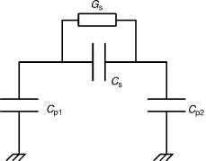
Depending on the technological steps used to fabricate the sensor, several parasitic capacitances Cp1,2 and conductances Gp may be present in the device and increase in importance as devices get smaller and the sensing capacitance Cs gets in the pF range. These parasitic effects may originate from various sources depending on the fabrication process used (i.e., stray capacitances of metal lines and connecting pads in parallel with the sensing capacitance or leakage resitors). Further variations may also be observed, due to technological reasons, between batches of the same sensor. In Fig. 9, a simple electrical model of a typical capacitive sensor, including parasitic effects, is shown. The spread in sensor characteristics (e.g., zero capacitance, sensitivity) resulting from these effects puts a great strain in the design of electronic interfaces for capacitive sensors. For this reason, most of the capacitive interfaces to date have been designed by taking into consideration the particular sensor and application that they are going to be used for. The design is a trade-off between power consumption, interface accuracy, and resolution, or even die size in some applications in the medical field.
A number of architectures have been proposed to date to convert capacitive changes into electrical signal. Some are built around a relaxation oscillator (46,48), others use switch capacitor techniques to convert capacitance changes
Figure 9. Simple electrical model of a capacitive sensor. Parasitic
capacitances is designated by Cp1,2, conductances by Gp and the sensing capacitance by Cs.
into voltage, and others interface the sensor directly into a sigma–delta modulator. A few attempts to develop a generic interface have also been reported (49,50). However, the power consumed is too high for remote sensing applications.
Van Der Goes and Meijer (49) presented a universal transducer interface for the read out of capacitors, platinum resistors, thermistors, resistive bridges, and potentiometers. The circuit uses the three signal technique in which the sensor signal Ex, a reference signal Eref, and the offset Eoff of the whole interface are measured in a identical way to achieve continuous autocalibration of offset and gain. The two port measurement technique is used to eliminate sensor parasitic capacitance. In this technique, a testing voltage, V, is forced on one capacitor electrode while current I is sensed on the other (51). The current I then depends only on the applied voltage and sensing capacitance. However, the technique is not energy efficient, since it requires four measurement cycles and three external voltage sources to determine the sensor capacitance.
Yazdi et al. (50) also developed a standardized switch capacitor interface for capacitive sensors, as shown in Fig. 10. This interface is capable of interfacing through a standard bus with a microcontroller that collects sensor data through the interface, calibrates data, and either stores or transmits it wirelessly or through a serial port. The readout circuit utilizes a low noise front-end charge integrator to read out the difference between the sensor capacitance and a reference capacitor. An input multiplexer allows for interfacing with up to six capacitive sensors. Finally, the chip can be digitally programmed to operate with one of three external or internal reference laser trimmable capacitors.
Bracke et al. (52) reports on a low power generic switched capacitor interface for capacitive sensors. The circuit uses a special clocking scheme, in which the analog sensor circuit block is clocked at a low 8 kHz frequency, while the sigma–delta modulator is clocked at 128 kHz. The technique ultimately reduces power consumption to 90 mW on the ON-state.
CAPACITIVE ELECTRONIC INTERFACES FOR IMPLANTABLE APPLICATIONS
In medical applications, where the diagnostic device is to be implanted inside the human body, only limited power is available for the electronic circuits and sensor. In such cases, power can only be found via a battery implanted together with the sensing system or through passive telemetry. In passive telemetry, energy may be harvested from a remote electromagnetic field transmitted outside the body. The same field may also be used to receive control data and transmit sensor data to a data logger. In both cases, minimizing power consumption is essential.
A simple low power interface for biomedical applications could be realized by using a simple relaxation oscillator (46,48). A capacitance-to-frequency modulated output was first proposed by Hanneborg et al. (46). This circuit delivers a digital pulse trail with frequency dependent on the sensor

8 CAPACITIVE MICROSENSORS FOR BIOMEDICAL APPLICATIONS
Figure 10. Circuit blocks of the capacitive electronic interface as described by W. Bracke et al. (50).
capacitance. The circuit consists of two current sources: a switch and a Schmitt trigger. The unknown capacitance is periodically charged and discharged by flipping the switch between current Iþ and I (Fig. 11).
An implementation of this type of capacitance-to-fre- quency converter is presented in Fig. 12. The circuit converts capacitance at its input into a frequency signal that can be readily fed to a digital microcontroller for processing. Either a capacitive sensor or a reference may be
Vdd
I+
VCx |
fx, fr |
I– Cx
GND
VCx
VOUT
Figure 11. Block diagram of the capacitive to frequency converter proposed by Hanneborg et al. (46). The circuit consists of two current sources, a switch and a Schmitt trigger.
switched in, and the frequency delivered at the circuit output is dependant on the input capacitance according to
f ¼ |
I0 |
(3) |
2CxVh |
where I0 is the current by which the sensor capacitance Cx is charged or discharged, and Vh is the hysteresis of the Schmitt trigger. The parameter Vc is a control signal that allows for switching between the unknown sensor capacitance Cx and a reference capacitor Cref. The output frequency when the reference is selected is independent of pressure, thus compensation of temperature and long-term drifts are possible by taking the ratio of the reference frequency and sensor frequency, Fref/Fsens.
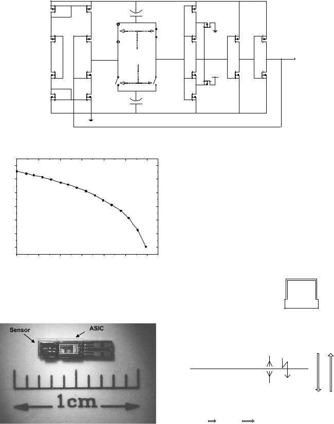
The response of a pressure measuring system based on this circuit realized in 1.2 mm of CMOS technology and a capacitive pressure sensor (53) is shown in Fig. 13. It operates at 4 V and draws 20 mA of average current. The system exhibits a sensitivity of 36 Hz/mmHg and is able to resolve pressure changes of 5 mmHg (0.66 kPa). A photograph of this system is shown in Fig. 14.
In medical science, however, there is often the need for long-term monitoring of vital life parameters. A good example is abdominal aortic aneurysm (AAA), which is a ballooning of the abdominal aorta. Patients who suffer from this condition need to undergo a procedure during which a stent graft is inserted. After the operation, however, it is possible that the aneurysmal sac is not completely isolated, leading to recurrent pressurization of the sac, a complication that, if left undetected, may lead to rupture of the sac and patient death. Long-term, postoperation monitoring of the patients is therefore necessary.
Early efforts for systems for the monitoring of blood pressure (54) used miniature active transmitters to transfer measured data and were battery powered, which limited
CAPACITIVE MICROSENSORS FOR BIOMEDICAL APPLICATIONS |
9 |
|
VDD |
|
|
M1 |
M5 |
|
|
|
Cx |
M9 |
M13 |
|
|
|
M15 |
M2 |
M6 |
|
M17 |
M10 |
|
||
|
|
|
|
|
Vc |
|
Fout |
|
|
|
|
M3 |
M7 |
|
VDD |
|
M18 |
||
|
M11 |
||
|
|
||
|
|
M16 |
|
|
|
|
|
M4 |
M8 |
|
M14 |
|
|
||
|
|
|
|
|
Cref |
M12 |
|
|
|
|
Figure 12. Schematic of Schmitt-trigger based oscillator used as a capacitive interface.
|
62 |
|
(kHz) |
60 |
|
58 |
||
Frequency |
||
56 |
||
|
54
52
50
0 |
50 |
100 |
150 |
200 |
250 |
300 |
Pressure change (mmHg)
Figure 13. Frequency response of a pressure measuring system consisting of the simple circuit of Fig. 12 and a capacitive pressure sensor in the range 0–300 mmHg ( 40 kPa).
their lifetime. An alternative approach to power these modules is through induction coupling, while the same radio frequency (RF) field can be used to transfer data out of the implanted module (55). The implanted circuit should be virtually immune to supply fluctuations arising from random misalignment of the implanted and the external coil. A new circuit was developed based on the previous architecture, but in which each circuit block was redesigned.
The block diagram of the passive telemetry system is depicted in Fig. 15. It consists of an external control unit (the base unit) and an implantable transponder. Wireless communication can then be established between the two units, based on an absorption modulation mechanism. The transponder receives power and external control data
Personal |
computer |
Figure 14. A photograph of a hybrid pressure measuring system consisting of a capacitive sensor and associated signal conditioning electronic circuit.
|
|
|
|
|
|
|
|
|
|
|
|
|
|
|
|
|
|
|
|
|
|
|
|
|
|
|
|
|
|
|
|
|
|
|
|
|
|
|
|
|
|
|
|
|
|
LCD |
|
|
RS232 |
||
|
|
|
|
|
|
|
|
|
|
|
|
|
|
|
|
|
|
|
|
Base unit |
|
|
|
|
|
|
|
|
|
|
|
|
|
|
|
Energy |
||
Skin |
|
|
|
|
|
|
|
|
|
|
|
|
|
|
|
|
|
|
|
RF field |
|||||
|
|
|
5 V |
|
|
|
|
|
|
|||
|
|
|
RF-DC |
|
|
|
|
|||||
|
|
|
Supply |
|
|
|
|
|||||
|
|
|
|
|
|
|
converter |
|
|
|
Data |
|
|
|
|
|
|
|
|
|
|
|
|||
|
|
|
|
|
|
|
|
|
|
|
|
|
|
|
|
|
|
|
|
|
|
|
|
|
|
|
|
|
|
|
|
|
RF |
|
|
|
|
|
Pressure |
|
C-F |
|
|
|
|
|
|
|
|||
|
|
|
modulator |
|
|
|
|
|||||
sensor |
|
converter |
|
|
|
|
|
|
|
|||
|
|
|
|
|
|
|
|
|
||||
|
|
|
|
|
|
|
|
|
|
|
|
|
Transponder
Figure 15. Block diagram of passive telemetry system.
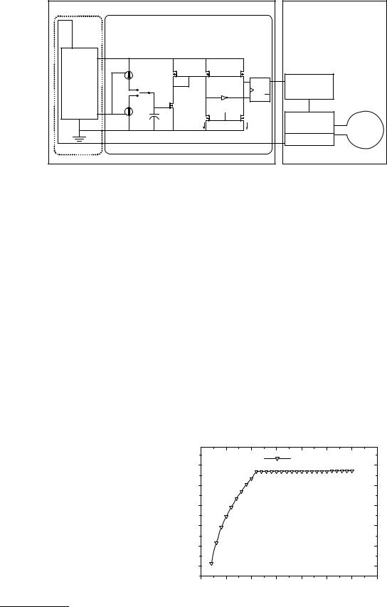
10 CAPACITIVE MICROSENSORS FOR BIOMEDICAL APPLICATIONS
C/F Chip |
Telemetry subsystem |
Bandgap |
|
Oscillator |
|
|
|
|
generator |
|
|
|
|
|
|
|
|
|
|
|
|
|
Vreg |
|
|
VREG |
|
|
|
|
|
|
|
|
|
|
|
|
MP1 |
MP2 |
MP3 |
|
|
|
Io |
|
|
S SET Q |
RF |
|
|
|
|
|
|
|
modulator |
|
|
|
|
R CLR Q |
Antenna |
|
Vbg |
Io |
MN1 |
Vbias |
MN3 |
RF/DC |
|
|
|
|
||||
|
Cx |
Il |
MN2 |
|||
|
I |
h |
converter |
|||
|
|
|
|
|
||
|
|
|
GND |
|
|
5 V regulator |
|
|
|
|
|
|
|
Figure 16. Transponder electronics. |
|
|
|
|
|
|
through an RF field, while it can transmit data by modulating the absorption rate. The base unit, on the other hand, demodulates the transmitted data and processes it though a microcontroller to convert the signal into an eight bit unsigned byte array. The resulting byte can then be sent to a PC through a serial output.
The block diagram of the transponder electronics is shown in Fig. 16. The improved capacitance-to-frequency circuit is used to interface a capacitive pressure sensor. The circuit consists of two basic blocks: a bandgap reference voltage generator and an oscillator. In order to achieve independence of the output frequency from the received power, this time the oscillator operates on an internally stabilized voltage generated from a bandgap reference. Voltage regulation is a critical part of telemetric systems as the induced power, and thus the voltage output, of the RF/dc converter in the transponder can greatly fluctuate in an actual implanted system becaused the relative position changes of the two antennas. In addition, to further immune the system from supply fluctuations a current mode comparator is used in the oscillator.
The bandgap reference voltage circuit is capable of operating at a low power supply as it operates on an internally regulated voltage VREG (56). This same node is also used for the supply of the oscillator circuit after the contributions of the extra branches of the oscillator are accounted for.
The oscillator itself is designed around a current mode comparator that results in an output frequency independent of power supply fluctuations and with small temperature drift. Triggering levels of this oscillator are defined by two currents: Ih and Il. The period of the output pulse can then be shown to be equal to
|
¼ |
I0 |
ðVbias VTNÞð |
|
|
|
Þ |
|
T |
|
2Cx |
|
pn |
|
1 |
|
(4) |
|
|
|
|
|
where n stands for the ratio of Ih to Il, and Vt is the threshold voltage. By taking the inverse of eq. 4 and substituting for I0, we obtain
Equation 5 implies that the output frequency is independent of the supply voltage and is dependent on temperature through the mobility term in k and the threshold voltage
Vt. Note also that the bias voltage Vbias is chosen to be equal to the bandgap reference voltage produced from the previous
stage, and is thus considered independent of voltage and temperature variations.
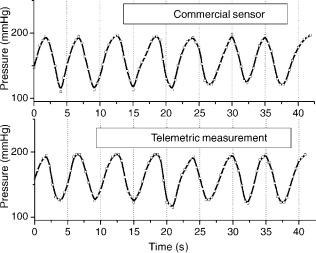
The C/F converter was designed and fabricated in 0.8 mm CMOS technology. A hybrid pressure measuring system composed of a capacitive pressure sensor (16) and the C/F chip. The system remains operational for a supply voltage down to 2.7 V and exhibiting high immunity to voltage variations from 3.7 to 5.5 V (Fig. 17). Simulated pressure pulses as those present in the aorta were measured using passive telemetry (Fig. 18).
CONCLUSIONS
Capacitive microsensors are in progressively increasing use in medical applications because of their advantages, such as small size, high sensitivity, and low power consumption. Silicon is the material of choice for these devices, which are finding applications for measuring pressure and
|
200 |
|
|
|
Cref connected |
|
||
|
|
|
|
|
|
|
|
|
(KHz) |
190 |
|
|
|
|
|
|
|
180 |
|
|
|
|
|
|
|
|
Frequency |
|
|
|
|
|
|
|
|
170 |
|
|
|
|
|
|
|
|
160 |
|
|
|
|
|
|
|
|
|
|
|
|
|
|
|
|
|
|
150 |
|
|
|
|
|
|
|
|
2.5 |
3.0 |
3.5 |
4.0 |
4.5 |
5.0 |
5.5 |
6.0 |
|
W0 |
|
|
|
|
VDDA (V) |
|
|
k |
|
ðVbias |
VTNÞ |
|
||
|
L0 |
|
|||||
f ¼ |
|
|
pn |
|
1 |
Þ |
(5) |
|
|
2Cxð |
|
Figure 17. Pressure measuring system frequency output. |
|||
CAPACITIVE MICROSENSORS FOR BIOMEDICAL APPLICATIONS |
11 |
Figure 18. Simulated pressure pulses as those present in the aorta measured using passive telemetry.
acceleration, but also in ultrasound imaging and microphones and for monitoring body analytes. Actually, although most of the existing devices are not integrated together with signal conditioning electronic circuits on the same chip, in the future it is expected that there will be an increasing integration scheme driven by the need of higher level miniaturization. Because of their low power consumption advantage, capacitive microsensors are of interest as implantable monitoring devices. An attractive application appears to be a miniaturized telemetry system that combines techniques for wireless power and data transfer to a capacitive sensor integrated with signal conditioning electronics.
BIBLIOGRAPHY
1.Tufte ON, Chapman PW, Long D. Silicon Diffused-Element Piezoresistive Diaphragm. J Appl Phys 1962;33:3322–3327.
2.Smith CS. Piezoresistance Effect in Germanium and Silicon. Phys Rev 1954;94:42.
3.Samaun X, Wise KD, Angel JB. An IC Piezoresistive Pressure Sensor for Biomedical Instrumentation. IEEE Trans Biomed Eng 1973;BME-20(2):101–109.
4.Ko WH, Hynelek J, Boettcher SF. Development of a miniature Pressure Transducer for Biomedical Application. IEEE Trans Electron Dev 1979;ED-26:1896.
5.Data Science Int., Roseville Minnesota.
6.Konigberg Instruments Inc. Pasadena, California.
7.Clark SK, Wise KD. Pressure sensitivity in anisotropically etched thindiaphragm pressure sensors. IEEE Trans Electron Dev 1979;ED-26(12):1887–1896.
8.Sander GS, Knutti JW, Meindl JD. A monolithic Capacitance Pressure Sensor with Pulse Periodic Output. IEEE Trans Electron Dev 1980;ED-27(5):927–930.
9.Lee YS, Wise KD. A batch-fabricated Silicon Capacitive Pressure Transducer with low temperature Sensitivity. IEEE Trans Electron Dev 1982;ED-29(1):42–47.
10.Backlund Y, Rosengren L, Ho¨k B. Passive Silicon Transensor Intended for biomedical, Remote Pressure monitoring. Sens Actuators 1990;A21(1–3):58–61.
11.Puers R, Peeters E, Van den Bossche A, Sansen W. A capacitive pressure sensor with low impedance output and active
supression of parasitic effects. Sens Actuators 1990;A21 (1-3):108–114.
12.Goosen JFL. Design considerations for silicon sensors for use in catheters and guide wires. Smart Mater Struct 2002; 11:804–812.
13.Goustouridis D, Chatzandroulis S, Normand P, Tsoukalas D. A miniature self-aligned pressure sensing element. J Micromech Microeng 1996;6:33–35.
14.Zhu YZ, Wang AB. Miniature fiber optic pressure sensor. IEEE Photonic Technol 2005;17(2):447–449.
15.Melva˚s P, Ka¨lvesten E, Enoksson P, Stemme G. A free-hang- ing strain-gauge for ultraminiaturized pressure sensors. Sens Actuators A 2002;97(8):75–82.
16.Chatzandroulis S, Tsoukalas D, Neukomm PA. A Miniature Pressure System with a Capacitive Sensor and a Passive Telemetry Link for Use in Implantable Applications. J MicroElectroMech S 2000;9(1):18–231.
17.Najafi N, Ludominky A. Initial Animal Studies of a Wireless, Batteryless, MEMS Implant for Cardiovascular Applications. Biomed Microdevices 2004;6(1):61–65.
18.Coosemans J, Catrysse M, Puers R. A readout circuit for an intra-ocular pressure sensor, Sens. Actuators A 2004;110 (1-3):432–438.
19.Hierold C, et al. Low power integrated pressure sensor for medical application. Sens Actuators A 1999;73(1–2):58–67.
20.Polliack AA, et al. Laboratory and clinical tests of a prototype pressure sensor for clinical assessment of prosthetic socket fit. Prosth Ortho Inter 2002;26(1):23–24.
21.Mu¨ ller O, Parak WJ, Wiedemann MG, Martini F. Threedimensional measurements of the pressure distribution in artificail joits with a capacitive sensor array. J Biomech 2004;37:1623–1625.
22.Luinge HJ, Veltink PH. Inclination measurement of human movement using a 30D accelerometer with autocalibration. IEEE T Neur Sys Reh 2004;12:112–121.
23.Puers R, Reyntjen S. Design and processing experiments of a new miniaturized capacitive triaxial accelerometer. Sens Actuators A 1998;68(1-3):324–328.
24.Lo¨tters JC, Olthuis W, Veltink PH, Bergveld P. Design, realization and characterization of a symmetrical triaxial capacitive accelerometer for medical application. Sens Actuators A 1997;61(1-3):303–308.
25.Huang Y, et al. Fabricating capacitive micromachined ultrasonic transducers with wafer-bonding technology. J Microelectromech S 2003;12(2):128–137.
26.Cianci E, et al. One-dimensional capacitative micromachined ultrasonic transducer arrays for echographic probes. Microelect Eng 2004;73–74:502–507.
27.Knight J, McLean J, Degertekin FL. Low Temperature Fabrication of Immersion Capacitive Micromachined Ultrasonic Transducers on Silicon and Dielectric Substrates. IEEE Trans UFFC 2004;51:1324–1333.
28.Rombach P, Mu¨ llenborn M, Klein U, Rasmussen K. The first low voltage, low noise differential silicon microphone, technology development and measurement results. Sens Actuators A 2002;95:196–201.
29.Pederson M, Olthuis W, Bergveld P. High-performance condenser microphone with fully integrated CMOS amplifier and DC-DC voltage converter. J MicroElectroMech S 1998;7(4): 387–394.
30.Strong ZA, Wang AW, McConaghy CF. Hydrogel-actuated capacitive transducer for wireless biosensors. Biomed Microdevices 2002;4(2):97–103.
31.Petersen KE. Silicon as a mechanical material. Proc IEEE 1982;70(5):420–457.
32.de Boer MJ, et al. Guidelines for etching silicon MEMS structures using fluorine high-density plasmas at cryogenic temperatures. J MicroElectroMech S 2002;11(4):385–401.