

- •Features
- •1. Pin Configurations
- •2. Overview
- •2.1 Block Diagram
- •2.2 Pin Descriptions
- •2.2.3 Port B (PB7:PB0) – XTAL1/XTAL2/TOSC1/TOSC2
- •2.2.4 Port C (PC5:PC0)
- •2.2.5 PC6/RESET
- •2.2.6 Port D (PD7:PD0)
- •2.2.7 RESET
- •2.2.9 AREF
- •2.2.10 ADC7:6 (TQFP and QFN/MLF Package Only)
- •3. Resources
- •4. Data Retention
- •5. About Code Examples
- •6. AVR CPU Core
- •6.1 Overview
- •6.2 Arithmetic Logic Unit – ALU
- •6.3 Status Register
- •6.3.1 SREG – The AVR Status Register
- •6.4 General Purpose Register File
- •6.5 Stack Pointer
- •6.5.1 SPH and SPL – Stack Pointer High and Low Register
- •6.6 Instruction Execution Timing
- •6.7 Reset and Interrupt Handling
- •6.7.1 Interrupt Response Time
- •7. AVR Memories
- •7.1 Overview
- •7.3 SRAM Data Memory
- •7.3.1 Data Memory Access Times
- •7.4 EEPROM Data Memory
- •7.4.1 EEPROM Read/Write Access
- •7.5 I/O Memory
- •7.6 Register Description
- •7.6.1 EEARH and EEARL – The EEPROM Address Register
- •7.6.2 EEDR – The EEPROM Data Register
- •7.6.3 EECR – The EEPROM Control Register
- •7.6.5 Preventing EEPROM Corruption
- •8. System Clock and Clock Options
- •8.1 Clock Systems and their Distribution
- •8.2 Clock Sources
- •8.3 Crystal Oscillator
- •8.5 External RC Oscillator
- •8.6 Calibrated Internal RC Oscillator
- •8.7 External Clock
- •8.8 Timer/Counter Oscillator
- •8.9 Register Description
- •8.9.1 OSCCAL – Oscillator Calibration Register
- •9. Power Management and Sleep Modes
- •9.1 Sleep Modes
- •9.2 Idle Mode
- •9.3 ADC Noise Reduction Mode
- •9.6 Standby Mode
- •9.7 Minimizing Power Consumption
- •9.7.2 Analog Comparator
- •9.7.4 Internal Voltage Reference
- •9.7.5 Watchdog Timer
- •9.7.6 Port Pins
- •9.8 Register Description
- •9.8.1 MCUCR – MCU Control Register
- •10. System Control and Reset
- •10.1 Resetting the AVR
- •10.2 Reset Sources
- •10.2.2 External Reset
- •10.2.4 Watchdog Reset
- •10.3 Internal Voltage Reference
- •10.4 Watchdog Timer
- •10.5 Timed Sequences for Changing the Configuration of the Watchdog Timer
- •10.5.1 Safety Level 1 (WDTON Fuse Unprogrammed)
- •10.5.2 Safety Level 2 (WDTON Fuse Programmed)
- •10.6 Register Description
- •10.6.1 MCUCSR – MCU Control and Status Register
- •10.6.2 WDTCR – Watchdog Timer Control Register
- •11. Interrupts
- •11.1 Interrupt Vectors in ATmega8A
- •11.1.1 Moving Interrupts Between Application and Boot Space
- •11.2 Register Description
- •11.2.1 GICR – General Interrupt Control Register
- •12. I/O Ports
- •12.1 Overview
- •12.2 Ports as General Digital I/O
- •12.2.1 Configuring the Pin
- •12.2.2 Reading the Pin Value
- •12.2.3 Digital Input Enable and Sleep Modes
- •12.2.4 Unconnected pins
- •12.3 Alternate Port Functions
- •12.3.1 SFIOR – Special Function IO Register
- •12.3.2 Alternate Functions of Port B
- •12.3.3 Alternate Functions of Port C
- •12.3.4 Alternate Functions of Port D
- •12.4 Register Description
- •12.4.1 PORTB – The Port B Data Register
- •12.4.2 DDRB – The Port B Data Direction Register
- •12.4.3 PINB – The Port B Input Pins Address
- •12.4.4 PORTC – The Port C Data Register
- •12.4.5 DDRC – The Port C Data Direction Register
- •12.4.6 PINC – The Port C Input Pins Address
- •12.4.7 PORTD – The Port D Data Register
- •12.4.8 DDRD – The Port D Data Direction Register
- •12.4.9 PIND – The Port D Input Pins Address
- •13. External Interrupts
- •13.1 Register Description
- •13.1.1 MCUCR – MCU Control Register
- •13.1.2 GICR – General Interrupt Control Register
- •13.1.3 GIFR – General Interrupt Flag Register
- •14. 8-bit Timer/Counter0
- •14.1 Features
- •14.2 Overview
- •14.2.1 Registers
- •14.2.2 Definitions
- •14.3 Timer/Counter Clock Sources
- •14.4 Counter Unit
- •14.5 Operation
- •14.6 Timer/Counter Timing Diagrams
- •14.7 Register Description
- •14.7.1 TCCR0 – Timer/Counter Control Register
- •14.7.2 TCNT0 – Timer/Counter Register
- •14.7.3 TIMSK – Timer/Counter Interrupt Mask Register
- •14.7.4 TIFR – Timer/Counter Interrupt Flag Register
- •15. Timer/Counter0 and Timer/Counter1 Prescalers
- •15.1 Overview
- •15.2 Internal Clock Source
- •15.3 Prescaler Reset
- •15.4 External Clock Source
- •15.5 Register Description
- •15.5.1 SFIOR – Special Function IO Register
- •16. 16-bit Timer/Counter1
- •16.1 Features
- •16.2 Overview
- •16.2.1 Registers
- •16.2.2 Definitions
- •16.2.3 Compatibility
- •16.3.1 Reusing the Temporary High Byte Register
- •16.4 Timer/Counter Clock Sources
- •16.5 Counter Unit
- •16.6 Input Capture Unit
- •16.6.1 Input Capture Pin Source
- •16.6.2 Noise Canceler
- •16.6.3 Using the Input Capture Unit
- •16.7 Output Compare Units
- •16.7.1 Force Output Compare
- •16.7.2 Compare Match Blocking by TCNT1 Write
- •16.7.3 Using the Output Compare Unit
- •16.8 Compare Match Output Unit
- •16.8.1 Compare Output Mode and Waveform Generation
- •16.9 Modes of Operation
- •16.9.1 Normal Mode
- •16.9.2 Clear Timer on Compare Match (CTC) Mode
- •16.9.3 Fast PWM Mode
- •16.9.4 Phase Correct PWM Mode
- •16.9.5 Phase and Frequency Correct PWM Mode
- •16.10 Timer/Counter Timing Diagrams
- •16.11 Register Description
- •16.11.1 TCCR1A – Timer/Counter 1 Control Register A
- •16.11.2 TCCR1B – Timer/Counter 1 Control Register B
- •16.11.3 TCNT1H and TCNT1L – Timer/Counter 1
- •16.11.4 OCR1AH and OCR1AL– Output Compare Register 1 A
- •16.11.5 OCR1BH and OCR1BL – Output Compare Register 1 B
- •16.11.6 ICR1H and ICR1L – Input Capture Register 1
- •17. 8-bit Timer/Counter2 with PWM and Asynchronous Operation
- •17.1 Features
- •17.2 Overview
- •17.2.1 Registers
- •17.2.2 Definitions
- •17.3 Timer/Counter Clock Sources
- •17.4 Counter Unit
- •17.5 Output Compare Unit
- •17.5.1 Force Output Compare
- •17.5.2 Compare Match Blocking by TCNT2 Write
- •17.5.3 Using the Output Compare Unit
- •17.6 Compare Match Output Unit
- •17.6.1 Compare Output Mode and Waveform Generation
- •17.7 Modes of Operation
- •17.7.1 Normal Mode
- •17.7.2 Clear Timer on Compare Match (CTC) Mode
- •17.7.3 Fast PWM Mode
- •17.7.4 Phase Correct PWM Mode
- •17.8 Timer/Counter Timing Diagrams
- •17.9 Asynchronous Operation of the Timer/Counter
- •17.9.1 Asynchronous Operation of Timer/Counter2
- •17.10 Timer/Counter Prescaler
- •17.11 Register Description
- •17.11.1 TCCR2 – Timer/Counter Control Register
- •17.11.2 TCNT2 – Timer/Counter Register
- •17.11.3 OCR2 – Output Compare Register
- •17.11.4 ASSR – Asynchronous Status Register
- •17.11.5 TIMSK – Timer/Counter Interrupt Mask Register
- •17.11.6 TIFR – Timer/Counter Interrupt Flag Register
- •17.11.7 SFIOR – Special Function IO Register
- •18. Serial Peripheral Interface – SPI
- •18.1 Features
- •18.2 Overview
- •18.3 SS Pin Functionality
- •18.3.1 Slave Mode
- •18.3.2 Master Mode
- •18.4 Data Modes
- •18.5 Register Description
- •18.5.1 SPCR – SPI Control Register
- •18.5.2 SPSR – SPI Status Register
- •18.5.3 SPDR – SPI Data Register
- •19. USART
- •19.1 Features
- •19.2 Overview
- •19.2.1 AVR USART vs. AVR UART – Compatibility
- •19.3 Clock Generation
- •19.3.1 Internal Clock Generation – The Baud Rate Generator
- •19.3.2 Double Speed Operation (U2X)
- •19.3.3 External Clock
- •19.3.4 Synchronous Clock Operation
- •19.4 Frame Formats
- •19.4.1 Parity Bit Calculation
- •19.5 USART Initialization
- •19.6 Data Transmission – The USART Transmitter
- •19.6.1 Sending Frames with 5 to 8 Data Bits
- •19.6.2 Sending Frames with 9 Data Bits
- •19.6.3 Transmitter Flags and Interrupts
- •19.6.4 Parity Generator
- •19.6.5 Disabling the Transmitter
- •19.6.6 Data Reception – The USART Receiver
- •Receiving Frames with 5 to 8 Data Bits
- •19.6.7 Receiving Frames with 9 Data Bits
- •19.6.8 Receive Compete Flag and Interrupt
- •19.6.9 Receiver Error Flags
- •19.6.10 Parity Checker
- •19.6.11 Disabling the Receiver
- •19.7 Asynchronous Data Reception
- •19.7.1 Asynchronous Clock Recovery
- •19.7.2 Asynchronous Data Recovery
- •19.7.3 Asynchronous Operational Range
- •19.8.1 Using MPCM
- •19.9 Accessing UBRRH/UCSRC Registers
- •19.9.1 Write Access
- •19.9.2 Read Access
- •19.10 Register Description
- •19.10.1 UDR– USART I/O Data Register
- •19.10.2 UCSRA – USART Control and Status Register A
- •19.10.3 UCSRB – USART Control and Status Register B
- •19.10.4 UCSRC – USART Control and Status Register C
- •19.10.5 UBRRL and UBRRH – USART Baud Rate Registers
- •19.11 Examples of Baud Rate Setting
- •20. Two-wire Serial Interface
- •20.1 Features
- •20.2 Overview
- •20.2.1 SCL and SDA Pins
- •20.2.2 Bit Rate Generator Unit
- •20.2.3 Bus Interface Unit
- •20.2.4 Address Match Unit
- •20.2.5 Control Unit
- •20.3.1 TWI Terminology
- •20.3.2 Electrical Interconnection
- •20.4 Data Transfer and Frame Format
- •20.4.1 Transferring Bits
- •20.4.2 START and STOP Conditions
- •20.4.3 Address Packet Format
- •20.4.4 Data Packet Format
- •20.4.5 Combining Address and Data Packets into a Transmission
- •20.6 Using the TWI
- •20.6.1 Transmission Modes
- •20.6.2 Master Transmitter Mode
- •20.6.3 Master Receiver Mode
- •20.6.4 Slave Receiver Mode
- •20.6.5 Slave Transmitter Mode
- •20.6.6 Miscellaneous States
- •20.6.7 Combining Several TWI Modes
- •20.8 Register Description
- •20.8.1 TWBR – TWI Bit Rate Register
- •20.8.2 TWCR – TWI Control Register
- •20.8.3 TWI Status Register – TWSR
- •20.8.4 TWDR – TWI Data Register
- •20.8.5 TWAR – TWI (Slave) Address Register
- •21. Analog Comparator
- •21.1 Overview
- •21.2 Analog Comparator Multiplexed Input
- •21.3 Register Description
- •21.3.1 SFIOR – Special Function IO Register
- •21.3.2 ACSR – Analog Comparator Control and Status Register
- •22. Analog-to-Digital Converter
- •22.1 Features
- •22.2 Overview
- •22.3 Starting a Conversion
- •22.4 Prescaling and Conversion Timing
- •22.5 Changing Channel or Reference Selection
- •22.5.1 ADC Input Channels
- •22.5.2 ADC Voltage Reference
- •22.6 ADC Noise Canceler
- •22.6.1 Analog Input Circuitry
- •22.6.2 Analog Noise Canceling Techniques
- •22.6.3 ADC Accuracy Definitions
- •22.7 ADC Conversion Result
- •22.8 Register Description
- •22.8.1 ADMUX – ADC Multiplexer Selection Register – ADMUX
- •22.8.2 ADCSRA – ADC Control and Status Register A
- •22.8.3 ADCL and ADCH – The ADC Data Register
- •23. Boot Loader Support – Read-While-Write Self-Programming
- •23.1 Features
- •23.2 Overview
- •23.3 Application and Boot Loader Flash Sections
- •23.3.1 Application Section
- •23.3.2 BLS – Boot Loader Section
- •23.5 Boot Loader Lock Bits
- •23.6 Entering the Boot Loader Program
- •23.8.1 Performing Page Erase by SPM
- •23.8.2 Filling the Temporary Buffer (Page Loading)
- •23.8.3 Performing a Page Write
- •23.8.4 Using the SPM Interrupt
- •23.8.5 Consideration While Updating BLS
- •23.8.7 Setting the Boot Loader Lock Bits by SPM
- •23.8.8 EEPROM Write Prevents Writing to SPMCR
- •23.8.9 Reading the Fuse and Lock Bits from Software
- •23.8.10 Preventing Flash Corruption
- •23.8.11 Programming Time for Flash when using SPM
- •23.8.12 Simple Assembly Code Example for a Boot Loader
- •23.8.13 Boot Loader Parameters
- •23.9 Register Description
- •23.9.1 Store Program Memory Control Register – SPMCR
- •24. Memory Programming
- •24.1 Program And Data Memory Lock Bits
- •24.2 Fuse Bits
- •24.2.1 Latching of Fuses
- •24.3 Signature Bytes
- •24.4 Calibration Byte
- •24.5 Page Size
- •24.6 Parallel Programming Parameters, Pin Mapping, and Commands
- •24.6.1 Signal Names
- •24.7 Parallel Programming
- •24.7.1 Enter Programming Mode
- •24.7.2 Considerations for Efficient Programming
- •24.7.3 Chip Erase
- •24.7.4 Programming the Flash
- •24.7.5 Programming the EEPROM
- •24.7.6 Reading the Flash
- •24.7.7 Reading the EEPROM
- •24.7.8 Programming the Fuse Low Bits
- •24.7.9 Programming the Fuse High Bits
- •24.7.10 Programming the Lock Bits
- •24.7.11 Reading the Fuse and Lock Bits
- •24.7.12 Reading the Signature Bytes
- •24.7.13 Reading the Calibration Byte
- •24.7.14 Parallel Programming Characteristics
- •24.8 Serial Downloading
- •24.9 Serial Programming Pin Mapping
- •24.9.1 Serial Programming Algorithm
- •24.9.2 Data Polling Flash
- •24.9.3 Data Polling EEPROM
- •24.9.4 SPI Serial Programming Characteristics
- •25. Electrical Characteristics
- •25.1 Absolute Maximum Ratings*
- •25.2 DC Characteristics
- •25.3 Speed Grades
- •25.4 Clock Characteristics
- •25.4.1 External Clock Drive Waveforms
- •25.4.2 External Clock Drive
- •25.5 System and Reset Characteristics
- •25.7 SPI Timing Characteristics
- •25.8 ADC Characteristics
- •26. Typical Characteristics
- •26.1 Active Supply Current
- •26.2 Idle Supply Current
- •26.5 Standby Supply Current
- •26.7 Pin Driver Strength
- •26.8 Pin Thresholds and Hysteresis
- •26.9 Bod Thresholds and Analog Comparator Offset
- •26.10 Internal Oscillator Speed
- •26.11 Current Consumption of Peripheral Units
- •26.12 Current Consumption in Reset and Reset Pulsewidth
- •27. Register Summary
- •28. Instruction Set Summary
- •29. Ordering Information
- •30. Packaging Information
- •31. Errata
- •31.1 ATmega8A, rev. L
- •32. Datasheet Revision History
- •Table of Contents

 ATmega8A
Figure 7-1. Program Memory Map
$000
Application Flash Section
Boot Flash Section
$FFF
7.3SRAM Data Memory
Figure 7-2 shows how the ATmega8A SRAM Memory is organized.
The lower 1120 Data memory locations address the Register File, the I/O Memory, and the internal data SRAM. The first 96 locations address the Register File and I/O Memory, and the next 1024 locations address the internal data SRAM.
The five different addressing modes for the Data memory cover: Direct, Indirect with Displacement, Indirect, Indirect with Pre-decrement, and Indirect with Post-increment. In the Register File, registers R26 to R31 feature the indirect addressing pointer registers.
The direct addressing reaches the entire data space.
The Indirect with Displacement mode reaches 63 address locations from the base address given by the Y- or Z-register.
When using register indirect addressing modes with automatic pre-decrement and post-incre- ment, the address registers X, Y and Z are decremented or incremented.
The 32 general purpose working registers, 64 I/O Registers, and the 1024 bytes of internal data SRAM in the ATmega8A are all accessible through all these addressing modes. The Register File is described in “General Purpose Register File” on page 10.
16
8159C–AVR–07/09
ATmega8A
Figure 7-2. Data Memory Map
Register File
R0
R1
R2
...
R29
R30
R31
I/O Registers
$00
$01
$02
...
$3D
$3E
$3F
Data Address Space
$0000
$0001
$0002
...
$001D
$001E
$001F
$0020
$0021
$0022
...
$005D
$005E
$005F
Internal SRAM
$0060
$0061
...
$045E
$045F
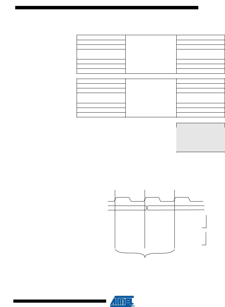
7.3.1Data Memory Access Times
This section describes the general access timing concepts for internal memory access. The internal data SRAM access is performed in two clkCPU cycles as described in Figure 7-3.
Figure 7-3. On-chip Data SRAM Access Cycles
T1 T2 T3
clkCPU |
|
|
Address |
Compute Address |
Address Valid |
Data 
WR 
Data 
RD 
Read Write
Memory Vccess Instruction |
Next Instruction |
17
8159C–AVR–07/09