- •Features
- •1. Pin Configurations
- •2. Overview
- •2.1 Block Diagram
- •2.2 Pin Descriptions
- •2.2.3 Port B (PB7:PB0) – XTAL1/XTAL2/TOSC1/TOSC2
- •2.2.4 Port C (PC5:PC0)
- •2.2.5 PC6/RESET
- •2.2.6 Port D (PD7:PD0)
- •2.2.7 RESET
- •2.2.9 AREF
- •2.2.10 ADC7:6 (TQFP and QFN/MLF Package Only)
- •3. Resources
- •4. Data Retention
- •5. About Code Examples
- •6. AVR CPU Core
- •6.1 Overview
- •6.2 Arithmetic Logic Unit – ALU
- •6.3 Status Register
- •6.3.1 SREG – The AVR Status Register
- •6.4 General Purpose Register File
- •6.5 Stack Pointer
- •6.5.1 SPH and SPL – Stack Pointer High and Low Register
- •6.6 Instruction Execution Timing
- •6.7 Reset and Interrupt Handling
- •6.7.1 Interrupt Response Time
- •7. AVR Memories
- •7.1 Overview
- •7.3 SRAM Data Memory
- •7.3.1 Data Memory Access Times
- •7.4 EEPROM Data Memory
- •7.4.1 EEPROM Read/Write Access
- •7.5 I/O Memory
- •7.6 Register Description
- •7.6.1 EEARH and EEARL – The EEPROM Address Register
- •7.6.2 EEDR – The EEPROM Data Register
- •7.6.3 EECR – The EEPROM Control Register
- •7.6.5 Preventing EEPROM Corruption
- •8. System Clock and Clock Options
- •8.1 Clock Systems and their Distribution
- •8.2 Clock Sources
- •8.3 Crystal Oscillator
- •8.5 External RC Oscillator
- •8.6 Calibrated Internal RC Oscillator
- •8.7 External Clock
- •8.8 Timer/Counter Oscillator
- •8.9 Register Description
- •8.9.1 OSCCAL – Oscillator Calibration Register
- •9. Power Management and Sleep Modes
- •9.1 Sleep Modes
- •9.2 Idle Mode
- •9.3 ADC Noise Reduction Mode
- •9.6 Standby Mode
- •9.7 Minimizing Power Consumption
- •9.7.2 Analog Comparator
- •9.7.4 Internal Voltage Reference
- •9.7.5 Watchdog Timer
- •9.7.6 Port Pins
- •9.8 Register Description
- •9.8.1 MCUCR – MCU Control Register
- •10. System Control and Reset
- •10.1 Resetting the AVR
- •10.2 Reset Sources
- •10.2.2 External Reset
- •10.2.4 Watchdog Reset
- •10.3 Internal Voltage Reference
- •10.4 Watchdog Timer
- •10.5 Timed Sequences for Changing the Configuration of the Watchdog Timer
- •10.5.1 Safety Level 1 (WDTON Fuse Unprogrammed)
- •10.5.2 Safety Level 2 (WDTON Fuse Programmed)
- •10.6 Register Description
- •10.6.1 MCUCSR – MCU Control and Status Register
- •10.6.2 WDTCR – Watchdog Timer Control Register
- •11. Interrupts
- •11.1 Interrupt Vectors in ATmega8A
- •11.1.1 Moving Interrupts Between Application and Boot Space
- •11.2 Register Description
- •11.2.1 GICR – General Interrupt Control Register
- •12. I/O Ports
- •12.1 Overview
- •12.2 Ports as General Digital I/O
- •12.2.1 Configuring the Pin
- •12.2.2 Reading the Pin Value
- •12.2.3 Digital Input Enable and Sleep Modes
- •12.2.4 Unconnected pins
- •12.3 Alternate Port Functions
- •12.3.1 SFIOR – Special Function IO Register
- •12.3.2 Alternate Functions of Port B
- •12.3.3 Alternate Functions of Port C
- •12.3.4 Alternate Functions of Port D
- •12.4 Register Description
- •12.4.1 PORTB – The Port B Data Register
- •12.4.2 DDRB – The Port B Data Direction Register
- •12.4.3 PINB – The Port B Input Pins Address
- •12.4.4 PORTC – The Port C Data Register
- •12.4.5 DDRC – The Port C Data Direction Register
- •12.4.6 PINC – The Port C Input Pins Address
- •12.4.7 PORTD – The Port D Data Register
- •12.4.8 DDRD – The Port D Data Direction Register
- •12.4.9 PIND – The Port D Input Pins Address
- •13. External Interrupts
- •13.1 Register Description
- •13.1.1 MCUCR – MCU Control Register
- •13.1.2 GICR – General Interrupt Control Register
- •13.1.3 GIFR – General Interrupt Flag Register
- •14. 8-bit Timer/Counter0
- •14.1 Features
- •14.2 Overview
- •14.2.1 Registers
- •14.2.2 Definitions
- •14.3 Timer/Counter Clock Sources
- •14.4 Counter Unit
- •14.5 Operation
- •14.6 Timer/Counter Timing Diagrams
- •14.7 Register Description
- •14.7.1 TCCR0 – Timer/Counter Control Register
- •14.7.2 TCNT0 – Timer/Counter Register
- •14.7.3 TIMSK – Timer/Counter Interrupt Mask Register
- •14.7.4 TIFR – Timer/Counter Interrupt Flag Register
- •15. Timer/Counter0 and Timer/Counter1 Prescalers
- •15.1 Overview
- •15.2 Internal Clock Source
- •15.3 Prescaler Reset
- •15.4 External Clock Source
- •15.5 Register Description
- •15.5.1 SFIOR – Special Function IO Register
- •16. 16-bit Timer/Counter1
- •16.1 Features
- •16.2 Overview
- •16.2.1 Registers
- •16.2.2 Definitions
- •16.2.3 Compatibility
- •16.3.1 Reusing the Temporary High Byte Register
- •16.4 Timer/Counter Clock Sources
- •16.5 Counter Unit
- •16.6 Input Capture Unit
- •16.6.1 Input Capture Pin Source
- •16.6.2 Noise Canceler
- •16.6.3 Using the Input Capture Unit
- •16.7 Output Compare Units
- •16.7.1 Force Output Compare
- •16.7.2 Compare Match Blocking by TCNT1 Write
- •16.7.3 Using the Output Compare Unit
- •16.8 Compare Match Output Unit
- •16.8.1 Compare Output Mode and Waveform Generation
- •16.9 Modes of Operation
- •16.9.1 Normal Mode
- •16.9.2 Clear Timer on Compare Match (CTC) Mode
- •16.9.3 Fast PWM Mode
- •16.9.4 Phase Correct PWM Mode
- •16.9.5 Phase and Frequency Correct PWM Mode
- •16.10 Timer/Counter Timing Diagrams
- •16.11 Register Description
- •16.11.1 TCCR1A – Timer/Counter 1 Control Register A
- •16.11.2 TCCR1B – Timer/Counter 1 Control Register B
- •16.11.3 TCNT1H and TCNT1L – Timer/Counter 1
- •16.11.4 OCR1AH and OCR1AL– Output Compare Register 1 A
- •16.11.5 OCR1BH and OCR1BL – Output Compare Register 1 B
- •16.11.6 ICR1H and ICR1L – Input Capture Register 1
- •17. 8-bit Timer/Counter2 with PWM and Asynchronous Operation
- •17.1 Features
- •17.2 Overview
- •17.2.1 Registers
- •17.2.2 Definitions
- •17.3 Timer/Counter Clock Sources
- •17.4 Counter Unit
- •17.5 Output Compare Unit
- •17.5.1 Force Output Compare
- •17.5.2 Compare Match Blocking by TCNT2 Write
- •17.5.3 Using the Output Compare Unit
- •17.6 Compare Match Output Unit
- •17.6.1 Compare Output Mode and Waveform Generation
- •17.7 Modes of Operation
- •17.7.1 Normal Mode
- •17.7.2 Clear Timer on Compare Match (CTC) Mode
- •17.7.3 Fast PWM Mode
- •17.7.4 Phase Correct PWM Mode
- •17.8 Timer/Counter Timing Diagrams
- •17.9 Asynchronous Operation of the Timer/Counter
- •17.9.1 Asynchronous Operation of Timer/Counter2
- •17.10 Timer/Counter Prescaler
- •17.11 Register Description
- •17.11.1 TCCR2 – Timer/Counter Control Register
- •17.11.2 TCNT2 – Timer/Counter Register
- •17.11.3 OCR2 – Output Compare Register
- •17.11.4 ASSR – Asynchronous Status Register
- •17.11.5 TIMSK – Timer/Counter Interrupt Mask Register
- •17.11.6 TIFR – Timer/Counter Interrupt Flag Register
- •17.11.7 SFIOR – Special Function IO Register
- •18. Serial Peripheral Interface – SPI
- •18.1 Features
- •18.2 Overview
- •18.3 SS Pin Functionality
- •18.3.1 Slave Mode
- •18.3.2 Master Mode
- •18.4 Data Modes
- •18.5 Register Description
- •18.5.1 SPCR – SPI Control Register
- •18.5.2 SPSR – SPI Status Register
- •18.5.3 SPDR – SPI Data Register
- •19. USART
- •19.1 Features
- •19.2 Overview
- •19.2.1 AVR USART vs. AVR UART – Compatibility
- •19.3 Clock Generation
- •19.3.1 Internal Clock Generation – The Baud Rate Generator
- •19.3.2 Double Speed Operation (U2X)
- •19.3.3 External Clock
- •19.3.4 Synchronous Clock Operation
- •19.4 Frame Formats
- •19.4.1 Parity Bit Calculation
- •19.5 USART Initialization
- •19.6 Data Transmission – The USART Transmitter
- •19.6.1 Sending Frames with 5 to 8 Data Bits
- •19.6.2 Sending Frames with 9 Data Bits
- •19.6.3 Transmitter Flags and Interrupts
- •19.6.4 Parity Generator
- •19.6.5 Disabling the Transmitter
- •19.6.6 Data Reception – The USART Receiver
- •Receiving Frames with 5 to 8 Data Bits
- •19.6.7 Receiving Frames with 9 Data Bits
- •19.6.8 Receive Compete Flag and Interrupt
- •19.6.9 Receiver Error Flags
- •19.6.10 Parity Checker
- •19.6.11 Disabling the Receiver
- •19.7 Asynchronous Data Reception
- •19.7.1 Asynchronous Clock Recovery
- •19.7.2 Asynchronous Data Recovery
- •19.7.3 Asynchronous Operational Range
- •19.8.1 Using MPCM
- •19.9 Accessing UBRRH/UCSRC Registers
- •19.9.1 Write Access
- •19.9.2 Read Access
- •19.10 Register Description
- •19.10.1 UDR– USART I/O Data Register
- •19.10.2 UCSRA – USART Control and Status Register A
- •19.10.3 UCSRB – USART Control and Status Register B
- •19.10.4 UCSRC – USART Control and Status Register C
- •19.10.5 UBRRL and UBRRH – USART Baud Rate Registers
- •19.11 Examples of Baud Rate Setting
- •20. Two-wire Serial Interface
- •20.1 Features
- •20.2 Overview
- •20.2.1 SCL and SDA Pins
- •20.2.2 Bit Rate Generator Unit
- •20.2.3 Bus Interface Unit
- •20.2.4 Address Match Unit
- •20.2.5 Control Unit
- •20.3.1 TWI Terminology
- •20.3.2 Electrical Interconnection
- •20.4 Data Transfer and Frame Format
- •20.4.1 Transferring Bits
- •20.4.2 START and STOP Conditions
- •20.4.3 Address Packet Format
- •20.4.4 Data Packet Format
- •20.4.5 Combining Address and Data Packets into a Transmission
- •20.6 Using the TWI
- •20.6.1 Transmission Modes
- •20.6.2 Master Transmitter Mode
- •20.6.3 Master Receiver Mode
- •20.6.4 Slave Receiver Mode
- •20.6.5 Slave Transmitter Mode
- •20.6.6 Miscellaneous States
- •20.6.7 Combining Several TWI Modes
- •20.8 Register Description
- •20.8.1 TWBR – TWI Bit Rate Register
- •20.8.2 TWCR – TWI Control Register
- •20.8.3 TWI Status Register – TWSR
- •20.8.4 TWDR – TWI Data Register
- •20.8.5 TWAR – TWI (Slave) Address Register
- •21. Analog Comparator
- •21.1 Overview
- •21.2 Analog Comparator Multiplexed Input
- •21.3 Register Description
- •21.3.1 SFIOR – Special Function IO Register
- •21.3.2 ACSR – Analog Comparator Control and Status Register
- •22. Analog-to-Digital Converter
- •22.1 Features
- •22.2 Overview
- •22.3 Starting a Conversion
- •22.4 Prescaling and Conversion Timing
- •22.5 Changing Channel or Reference Selection
- •22.5.1 ADC Input Channels
- •22.5.2 ADC Voltage Reference
- •22.6 ADC Noise Canceler
- •22.6.1 Analog Input Circuitry
- •22.6.2 Analog Noise Canceling Techniques
- •22.6.3 ADC Accuracy Definitions
- •22.7 ADC Conversion Result
- •22.8 Register Description
- •22.8.1 ADMUX – ADC Multiplexer Selection Register – ADMUX
- •22.8.2 ADCSRA – ADC Control and Status Register A
- •22.8.3 ADCL and ADCH – The ADC Data Register
- •23. Boot Loader Support – Read-While-Write Self-Programming
- •23.1 Features
- •23.2 Overview
- •23.3 Application and Boot Loader Flash Sections
- •23.3.1 Application Section
- •23.3.2 BLS – Boot Loader Section
- •23.5 Boot Loader Lock Bits
- •23.6 Entering the Boot Loader Program
- •23.8.1 Performing Page Erase by SPM
- •23.8.2 Filling the Temporary Buffer (Page Loading)
- •23.8.3 Performing a Page Write
- •23.8.4 Using the SPM Interrupt
- •23.8.5 Consideration While Updating BLS
- •23.8.7 Setting the Boot Loader Lock Bits by SPM
- •23.8.8 EEPROM Write Prevents Writing to SPMCR
- •23.8.9 Reading the Fuse and Lock Bits from Software
- •23.8.10 Preventing Flash Corruption
- •23.8.11 Programming Time for Flash when using SPM
- •23.8.12 Simple Assembly Code Example for a Boot Loader
- •23.8.13 Boot Loader Parameters
- •23.9 Register Description
- •23.9.1 Store Program Memory Control Register – SPMCR
- •24. Memory Programming
- •24.1 Program And Data Memory Lock Bits
- •24.2 Fuse Bits
- •24.2.1 Latching of Fuses
- •24.3 Signature Bytes
- •24.4 Calibration Byte
- •24.5 Page Size
- •24.6 Parallel Programming Parameters, Pin Mapping, and Commands
- •24.6.1 Signal Names
- •24.7 Parallel Programming
- •24.7.1 Enter Programming Mode
- •24.7.2 Considerations for Efficient Programming
- •24.7.3 Chip Erase
- •24.7.4 Programming the Flash
- •24.7.5 Programming the EEPROM
- •24.7.6 Reading the Flash
- •24.7.7 Reading the EEPROM
- •24.7.8 Programming the Fuse Low Bits
- •24.7.9 Programming the Fuse High Bits
- •24.7.10 Programming the Lock Bits
- •24.7.11 Reading the Fuse and Lock Bits
- •24.7.12 Reading the Signature Bytes
- •24.7.13 Reading the Calibration Byte
- •24.7.14 Parallel Programming Characteristics
- •24.8 Serial Downloading
- •24.9 Serial Programming Pin Mapping
- •24.9.1 Serial Programming Algorithm
- •24.9.2 Data Polling Flash
- •24.9.3 Data Polling EEPROM
- •24.9.4 SPI Serial Programming Characteristics
- •25. Electrical Characteristics
- •25.1 Absolute Maximum Ratings*
- •25.2 DC Characteristics
- •25.3 Speed Grades
- •25.4 Clock Characteristics
- •25.4.1 External Clock Drive Waveforms
- •25.4.2 External Clock Drive
- •25.5 System and Reset Characteristics
- •25.7 SPI Timing Characteristics
- •25.8 ADC Characteristics
- •26. Typical Characteristics
- •26.1 Active Supply Current
- •26.2 Idle Supply Current
- •26.5 Standby Supply Current
- •26.7 Pin Driver Strength
- •26.8 Pin Thresholds and Hysteresis
- •26.9 Bod Thresholds and Analog Comparator Offset
- •26.10 Internal Oscillator Speed
- •26.11 Current Consumption of Peripheral Units
- •26.12 Current Consumption in Reset and Reset Pulsewidth
- •27. Register Summary
- •28. Instruction Set Summary
- •29. Ordering Information
- •30. Packaging Information
- •31. Errata
- •31.1 ATmega8A, rev. L
- •32. Datasheet Revision History
- •Table of Contents
ATmega8A
8.1.3Flash Clock – clkFLASH
The Flash clock controls operation of the Flash interface. The Flash clock is usually active simultaneously with the CPU clock.
8.1.4Asynchronous Timer Clock – clkASY
The Asynchronous Timer clock allows the Asynchronous Timer/Counter to be clocked directly from an external 32 kHz clock crystal. The dedicated clock domain allows using this Timer/Counter as a real-time counter even when the device is in sleep mode. The Asynchronous Timer/Counter uses the same XTAL pins as the CPU main clock but requires a CPU main clock frequency of more than four times the Oscillator frequency. Thus, asynchronous operation is only available while the chip is clocked on the Internal Oscillator.
8.1.5ADC Clock – clkADC
The ADC is provided with a dedicated clock domain. This allows halting the CPU and I/O clocks in order to reduce noise generated by digital circuitry. This gives more accurate ADC conversion results.
8.2Clock Sources
The device has the following clock source options, selectable by Flash Fuse Bits as shown below. The clock from the selected source is input to the AVR clock generator, and routed to the appropriate modules.
Table 8-1. |
Device Clocking Options Select(1) |
|
|
Device Clocking Option |
|
CKSEL3:0 |
|
|
|
|
|
External Crystal/Ceramic Resonator |
|
1111 - 1010 |
|
|
|
|
|
External Low-frequency Crystal |
|
1001 |
|
|
|
|
|
External RC Oscillator |
|
1000 - 0101 |
|
|
|
|
|
Calibrated Internal RC Oscillator |
|
0100 - 0001 |
|
|
|
|
|
External Clock |
|
0000 |
|
|
|
|
|
Note: 1. |
For all fuses “1” means unprogrammed while “0” means programmed. |
|
The various choices for each clocking option is given in the following sections. When the CPU wakes up from Power-down or Power-save, the selected clock source is used to time the startup, ensuring stable Oscillator operation before instruction execution starts. When the CPU starts from reset, there is as an additional delay allowing the power to reach a stable level before commencing normal operation. The Watchdog Oscillator is used for timing this real-time part of the start-up time. The number of WDT Oscillator cycles used for each time-out is shown in Table 8- 2. The frequency of the Watchdog Oscillator is voltage dependent as shown in “Typical Characteristics”. The device is shipped with CKSEL = “0001” and SUT = “10” (1 MHz Internal RC Oscillator, slowly rising power).
Table 8-2. |
Number of Watchdog Oscillator Cycles |
|
|
|
Typical Time-out (VCC = 5.0V) |
Typical Time-out (VCC = 3.0V) |
Number of Cycles |
||
|
4.1 ms |
4.3 ms |
4K |
(4,096) |
|
|
|
|
|
|
65 ms |
69 ms |
64K |
(65,536) |
|
|
|
|
|
25
8159C–AVR–07/09
ATmega8A
8.3Crystal Oscillator
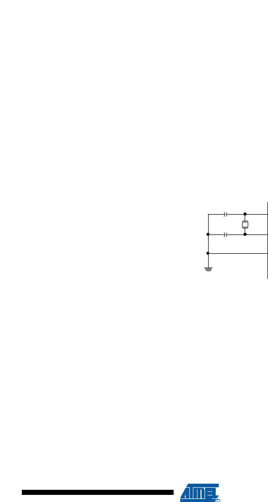
XTAL1 and XTAL2 are input and output, respectively, of an inverting amplifier which can be configured for use as an On-chip Oscillator, as shown in Figure 8-2. Either a quartz crystal or a ceramic resonator may be used. The CKOPT Fuse selects between two different Oscillator amplifier modes. When CKOPT is programmed, the Oscillator output will oscillate a full rail-to- rail swing on the output. This mode is suitable when operating in a very noisy environment or when the output from XTAL2 drives a second clock buffer. This mode has a wide frequency range. When CKOPT is unprogrammed, the Oscillator has a smaller output swing. This reduces power consumption considerably. This mode has a limited frequency range and it cannot be used to drive other clock buffers.
For resonators, the maximum frequency is 8 MHz with CKOPT unprogrammed and 16 MHz with CKOPT programmed. C1 and C2 should always be equal for both crystals and resonators. The optimal value of the capacitors depends on the crystal or resonator in use, the amount of stray capacitance, and the electromagnetic noise of the environment. Some initial guidelines for choosing capacitors for use with crystals are given in Table 8-3. For ceramic resonators, the capacitor values given by the manufacturer should be used.
Figure 8-2. Crystal Oscillator Connections
C2
XTAL2
C1
XTAL1
GND
The Oscillator can operate in three different modes, each optimized for a specific frequency range. The operating mode is selected by the fuses CKSEL3:1 as shown in Table 8-3.
Table 8-3. |
Crystal Oscillator Operating Modes |
|
|
|
|
Frequency |
Recommended Range for Capacitors C1 |
CKOPT |
CKSEL3:1 |
Range(MHz) |
and C2 for Use with Crystals (pF) |
|
|
|
|
1 |
101(1) |
0.4 - 0.9 |
– |
1 |
110 |
0.9 - 3.0 |
12 - 22 |
|
|
|
|
1 |
111 |
3.0 - 8.0 |
12 - 22 |
|
|
|
|
0 |
101, 110, 111 |
1.0 ≤ |
12 - 22 |
|
|
|
|
Note: 1. |
This option should not be used with crystals, only with ceramic resonators. |
The CKSEL0 Fuse together with the SUT1:0 Fuses select the start-up times as shown in Table 8-4.
26
8159C–AVR–07/09
ATmega8A
Table 8-4. |
Start-up Times for the Crystal Oscillator Clock Selection |
||||
|
|
Start-up Time |
Additional Delay |
|
|
|
|
from Power-down |
from Reset |
|
|
CKSEL0 |
SUT1:0 |
and Power-save |
(VCC = 5.0V) |
Recommended Usage |
|
0 |
00 |
258 CK(1) |
4.1 ms |
Ceramic resonator, fast rising |
|
power |
|||||
|
|
|
|
||
|
|
|
|
|
|
0 |
01 |
258 CK(1) |
65 ms |
Ceramic resonator, slowly |
|
rising power |
|||||
|
|
|
|
||
|
|
|
|
|
|
0 |
10 |
1K CK(2) |
– |
Ceramic resonator, BOD |
|
enabled |
|||||
|
|
|
|
||
|
|
|
|
|
|
0 |
11 |
1K CK(2) |
4.1 ms |
Ceramic resonator, fast rising |
|
power |
|||||
|
|
|
|
||
|
|
|
|
|
|
1 |
00 |
1K CK(2) |
65 ms |
Ceramic resonator, slowly |
|
rising power |
|||||
|
|
|
|
||
|
|
|
|
|
|
1 |
01 |
16K CK |
– |
Crystal Oscillator, BOD |
|
enabled |
|||||
|
|
|
|
||
|
|
|
|
|
|
1 |
10 |
16K CK |
4.1 ms |
Crystal Oscillator, fast rising |
|
power |
|||||
|
|
|
|
||
|
|
|
|
|
|
1 |
11 |
16K CK |
65 ms |
Crystal Oscillator, slowly |
|
rising power |
|||||
|
|
|
|
||
|
|
|
|
|
Notes: 1. These options should only be used when not operating close to the maximum frequency of the device, and only if frequency stability at start-up is not important for the application. These options are not suitable for crystals.
2.These options are intended for use with ceramic resonators and will ensure frequency stability at start-up. They can also be used with crystals when not operating close to the maximum frequency of the device, and if frequency stability at start-up is not important for the application.
8.4Low-frequency Crystal Oscillator
To use a 32.768 kHz watch crystal as the clock source for the device, the Low-frequency Crystal Oscillator must be selected by setting the CKSEL Fuses to “1001”. The crystal should be connected as shown in Figure 8-2. By programming the CKOPT Fuse, the user can enable internal capacitors on XTAL1 and XTAL2, thereby removing the need for external capacitors. The internal capacitors have a nominal value of 36 pF.
When this Oscillator is selected, start-up times are determined by the SUT Fuses as shown in Table 8-5.
Table 8-5. |
Start-up Times for the Low-frequency Crystal Oscillator Clock Selection |
|||
|
Start-up Time from |
Additional Delay |
|
|
|
Power-down and |
from Reset |
|
|
SUT1:0 |
Power-save |
(VCC = 5.0V) |
|
Recommended Usage |
00 |
1K CK(1) |
4.1 ms |
|
Fast rising power or BOD enabled |
01 |
1K CK(1) |
65 ms |
|
Slowly rising power |
10 |
32K CK |
65 ms |
|
Stable frequency at start-up |
|
|
|
|
|
11 |
|
Reserved |
|
|
|
|
|
|
|
Note: 1. |
These options should only be used if frequency stability at start-up is not important for the |
|||
|
application. |
|
|
|
27
8159C–AVR–07/09
ATmega8A
8.5External RC Oscillator
For timing insensitive applications, the external RC configuration shown in Figure 8-3 can be used. The frequency is roughly estimated by the equation f = 1/(3RC). C should be at least 22 pF. By programming the CKOPT Fuse, the user can enable an internal 36 pF capacitor between XTAL1 and GND, thereby removing the need for an external capacitor.
Figure 8-3. External RC Configuration
|
VCC |
|
|||
R |
|
NC |
|
|
XTAL2 |
|
|||||
|
|
||||
|
|
|
|
|
|
|
|
|
|
|
XTAL1 |
|
|
|
|
|
|
|
|
|
|
|
C
GND
The Oscillator can operate in four different modes, each optimized for a specific frequency range. The operating mode is selected by the fuses CKSEL3:0 as shown in Table 8-6.
Table 8-6. |
External RC Oscillator Operating Modes |
|
|
|
CKSEL3:0 |
|
Frequency Range (MHz) |
|
|
|
|
|
0101 |
|
0.1 - 0.9 |
|
|
|
|
|
0110 |
|
0.9 - 3.0 |
|
|
|
|
|
0111 |
|
3.0 - 8.0 |
|
|
|
|
|
1000 |
|
8.0 - 12.0 |
|
|
|
|
When this Oscillator is selected, start-up times are determined by the SUT Fuses as shown in Table 8-7.
Table 8-7. |
Start-up Times for the External RC Oscillator Clock Selection |
||
|
Start-up Time from |
Additional Delay |
|
|
Power-down and |
from Reset |
|
SUT1:0 |
Power-save |
(VCC = 5.0V) |
Recommended Usage |
00 |
18 CK |
– |
BOD enabled |
|
|
|
|
01 |
18 CK |
4.1 ms |
Fast rising power |
|
|
|
|
10 |
18 CK |
65 ms |
Slowly rising power |
|
|
|
|
11 |
6 CK(1) |
4.1 ms |
Fast rising power or BOD enabled |
Note: 1. |
This option should not be used when operating close to the maximum frequency of the device. |
28
8159C–AVR–07/09