

Ersoy O.K. Diffraction, Fourier optics, and imaging (Wiley, 2006)(ISBN 0471238163)(427s) PEo
.pdf178 |
OPTICAL DEVICES BASED ON WAVE MODULATION |
emulsion is sandwiched between a protective layer and a base consisting of acetate or mylar for films and glass for plates. In black-and-white photographic film, there is typically one layer of silver grains. In color film, there are at least three such layers. Dyes added to the silver grains make the crystals sensitive to different colors.
Modulation of light occurs as follows:
1.If a photon is absorbed by a silver halide grain, an electron–hole pair is generated within the grain.
2.A generated electron is in the conduction band and hence moves around in the crystal and may become trapped at a crystal dislocation.
3.A trapped electron attracts a mobile silver ion. This results in a single atom of metallic silver with a lifetime of the order of a few seconds.
4.Several additional silver atoms may be formed at the same site. At least four silver atoms called silver speck are needed for the development process.
The development is done in a chemical bath. The developer acts on the silver specks and causes the entire crystal to be reduced to metallic silver in regions where enough light has been absorbed. Those regions that did not turn to metallic silver will eventually do so and hence must be removed by a process called fixing. This involves immersing the transparency in a second chemical bath.
The terms used in connection with the usage of photographic films and their definitions are discussed below.
Exposure Eðx; yÞ |
|
|
|
|
|
Eðx; yÞ ¼ Ieðx; yÞT |
ð11:1-1Þ |
||||
where |
|
|
|
|
|
Ieðx; yÞ ¼ intensity incident on the film during exposure |
|
||||
T ¼ exposure time |
2 |
|
|
|
|
Eðx; yÞ is usually in units of mJ/cm |
|
. |
|
|
|
Intensity Transmittance aðx; yÞ |
|
|
|
|
|
|
|
|
x y |
|
|
aðx; yÞ ¼ local average |
Ið ; Þ |
|
ð11:1-2Þ |
||
Ieðx; yÞ |
|||||
where
Iðx; yÞ ¼ intensity transmitted by the transparency after development Iiðx; yÞ ¼ incident intensity
Photographic Density
Silver mass per unit area is approximately proportional to the photographic density D, which is defined as the logarithm of the reciprocal of the intensity transmittance of a photographic transparency. Thus, D is given by
1 |
ð11:1-3Þ |
D ¼ log10 a |
TRANSMITTANCE OF LIGHT BY FILM |
179 |
|||||
|
|
|
|
|
|
|
|
|
|
|
|
|
|
|
|
|
|
|
|
|
|
|
|
|
|
|
|
|
|
|
|
|
|
|
|
|
|
|
|
|
|
|
|
|
|
|
|
|
|
|
|
|
|
|
|
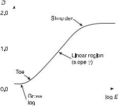
Figure 11.1. The Hurter–Driffield curve for photographic emulsion.
This can also be written as
a ¼ |
10 D |
ð |
11:1-4 |
Þ |
|
|
Hurter–Driffield (H & D) Curve
The H & D curve is the plot of D versus log E. A typical H & D curve for a negative film is shown in Figure 11.1. Note that the density is essentially constant for very low exposures and very high exposures. In between, there is the linear region, which is the most commonly used region in photography.
Gamma
The gamma g of the emulsion is the slope of the H & D curve in the linear region. A high-contrast film has a large gamma (typically 2 or 3), and a low-contrast film has a small gamma (1 or less). g is positive for a negative film and negative for a positive film.
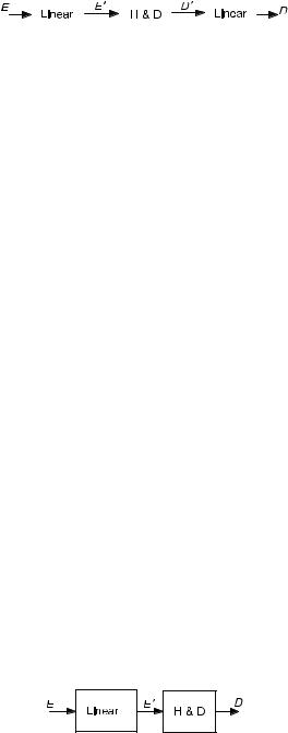
11.3TRANSMITTANCE OF LIGHT BY FILM
In incoherent and coherent optical systems, film is often used to modulate the transmittance of light. How this is achieved depends on whether coherent or incoherent light is used. Both these cases are discussed below.
Incoherent Light
In the linear region of the H & D curve, which is assumed to be used, the density can be written as [Goodman]
|
1 |
|
|
|
D ¼ g log10ðEÞ D0 ¼ log10 |
|
|
|
ð11:3-1Þ |
a |
||||

180 |
OPTICAL DEVICES BASED ON WAVE MODULATION |
||||
or |
|
|
|
|
|
|
log10ðaÞ ¼ g log10ðEÞ þ D0 |
ð11:3-2Þ |
|||
As E equals IeT, we obtain |
|
|
|
|
|
|
a ¼ |
K I g |
ð |
11:3-3 |
Þ |
|
|
|
|||
where K ¼ 10D0 T g is a positive constant. Equation (11.3-3) shows that transmittance depends nonlinearly on the incident intensity and decreases as increases for positive g.
EXAMPLE 11.1 Show that two negative films in tandem results in transmittance I increasing with incident intensity.
Solution: The first film has transmittance given by
a1 ¼ K1I1 g1
where I1 is the intensity of the illuminating beam.
Suppose the first film is placed in contact with the second unexposed film and illuminated with intensity I2. The intensity incident on the second emulsion equals a1I2. The intensity transmittance a2 can be written as
a2 ¼ K2ða1I2Þ g2 ¼ K I1g1g2
where
K ¼ K1K2
It is seen that the overall transmittance a2 increases with I1.
Coherent Light
With coherent light, phase modulation also becomes important. Phase modulation is caused by variations of the film or plate thickness. The amplitude transmittance of the film can be written as
|
ð |
|
Þ ¼ p |
ð |
|
Þ |
ac |
|
x; y |
aðx; yÞejfðx;yÞ |
|
11:3-4 |
|
where fðx; yÞ is the phase due to thickness variation.
The phase term ejfðx;yÞ is usually undesirable. It is possible to remove it by using a liquid gate. This is schematically shown in Figure 11.2.

184 |
OPTICAL DEVICES BASED ON WAVE MODULATION |
bandpass filter. In other words, no relief is produced at very low or very high spatial frequencies. For a 15 mm thick emulsion, the peak thickness variations of the order of 1–2 mm occur at about 10 cycles/mm [Goodman].
The nontanning bleach results in internal refractive index changes within the emulsion. The resulting transparency represents a spatial modulation of phase through variations in the index of refraction.
11.6 DIFFRACTIVE OPTICS, BINARY OPTICS, AND DIGITAL OPTICS
Conventional optical devices such as lenses, mirrors, and prisms are based on refraction or reflection. By contrast, diffractive optical elements (DOEs), for example, in the form of a phase relief, are based on diffraction. The important advantages of DOEs are as follows:
1.A DOE can perform more than one function, for example, have multiple focal points, corresponding to multiple lenses on a single element. It can also be designed for use with multiple wavelengths.
2.DOEs are generally much lighter and occupy less volume than refractive and reflective optical elements.
3.With mass manufacturing, they are expected to be less expensive.
As DOEs are based on diffraction, they are highly dispersive, namely, their properties depend on wavelength. Hence they are more commonly used with monochromatic light. However, the dispersive properties can also be used to advantage. For example, light at one wavelength can be focused at one point, and light at another wavelength can be focused at another point in space. In addition, refractive and diffractive optical elements can be combined in such a way that wavelength dispersion can be removed, and goals such as removal of spherical aberration can be achieved. The topics of diffractive optics and design of DOEs are covered in detail in Chapters 15 and 16.
Diffractive optics, binary optics, and digital optics often refer to the same modulation techniques and technologies of implementation. In all cases, lithography and micromachining techniques are of paramount importance for the implementation of very novel devices for various applications. These are also technologies for VLSI and integrated optics as well as other nano/micro applications. At the other extreme, laser printers can be used to text designs at low resolution [Asakura, Nagashima, 1976].
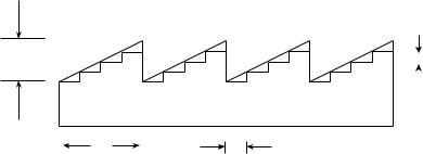
Even though the word binary is used, quantization, for example, of phase involves a number of levels such as 2, 4, or 8 levels of quantization. Quantization of phase is usually achieved by modulating the thickness of a DOE in quantized steps. 2N discrete levels of phase are usually used. For example, consider a blazed grating shown in Figure 11.9. Such a grating has 100% diffraction efficiency, meaning that
E-BEAM LITHOGRAPHY |
185 |
∆0 |
|
|
∆0L/(2N) |
|
|
||
|
|
||
|
|
|
|
L
L/(2N)
Figure 11.8. Approximation of a blazed grating by N ¼ 2M phase levels.
all the wave goes into the first order of diffraction if continuous modulation of thickness to generate the desired phase profile is undertaken. In binary optics, this is approximated by N ¼ 2M levels, say, M ¼ 2 is used as shown in Figure 11.8. E-beam and reactive ion etching techniques of fabricating such an element are discussed in the next section.
In recent years, another technology to fabricate DOE’s has been micromachining by femtosecond laser pulses in transparent materials such as silica glass [Watanebe et al., 2002], [Yin et al., 2005]. The intensity of the femtosecond laser pulses in the focal region is high enough to modify the index of refraction while other regions remain unaffected. This phenomenon allows fabrication of a variety of diffractive and photonic devices in glass. A very interesting advantage here is the relative ease of guiding the focused beam within a volume.
11.7E-BEAM LITHOGRAPHY
Lithography refers to a number of technologies used to print patterns onto a substrate. The most common application is printing the patterns of integrated circuits onto a semiconductor substrate. Advanced lithographic techniques include optical lithography, electron-beam (e-beam) lithography, extreme ultraviolet (EUVL) lithography, and x-ray lithography [Bowden et al., 1983].
There are two basic steps involved in lithography. The first step is to create a desired pattern. The second is to transfer this pattern into the substrate. The quality of a lithographic method is measured primarily by its resolution. Resolution is the minimum feature size that can be obtained. Resolution is determined not only by the lithography method, but also by the ability of the resist to reconstruct the pattern.
E-beam lithography is a high-resolution technology to generate custom-made DOEs. It utilizes an intense and uniform electron source with a small spot size, high stability, and long life. The main attributes of e-beam lithography technology are as follows: (1) It is capable of very high resolution; (2) it works with a variety of materials and patterns; (3) it is slow compared to optical lithography; and (4) it is
186 |
OPTICAL DEVICES BASED ON WAVE MODULATION |
expensive. Combined with reactive ion etching (RIE), creation of DOEs with very fine resolution and high efficiency is possible.
As an example, consider a binary phase DOE consisting of a 2-D array of small apertures that can be assumed to be sampled points. At each such point, a phase shift of either 0 or 180 degrees is to be generated. At points where a 180 degree phase shift is desired, the substrate is etched to the required depth. The e-beam exposes a pattern onto an e-beam sensitive resist indicating where apertures are to be made, and RIE is used to etch the apertures to the desired depth. This can also be achieved by chemical processing, but RIE is a higher precision technology. This approach can be generalized to any number of phase quantization levels in powers of 2.
A typical e-beam machine is capable of generating a beam with a spot size around 10 nm. Therefore, it is capable of exposing patterns with lines of widths less than 0.1 mm or 100 nm. For binary phase DOEs, each square aperture has a size of approximately 1 mm 1 mm. For such feature sizes around, a total pattern size of, say, 1 mm 1 mm can be achieved, while maintaining high resolution. Larger patterns are generated by stitching together a number of such patterns together under interferometric control.
Dry etching systems are capable of generating very fine surface relief. For example, 180 degree phase change needed for binary phase DOEs occurs over a distance of half a wavelength. For visible light, that corresponds to a length of the
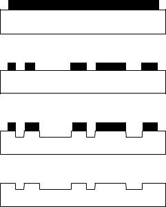
(1) Spin on electron resist.
(2) Expose resist with e-beam and develop.
(3)Reactive ion-etch.
(4)Remove remaining resist.
Figure 11.9. The experimental procedure to implement a DOE with e-beam and reactive ion etching systems.
E-BEAM LITHOGRAPHY |
187 |
order of half a micron. RIE makes it possible to induce surface relief of such small dimensions with very high accuracy.
11.7.1DOE Implementation
The basic procedure for producing a binary phase hologram using e-beam lithography is illustrated in Figure 11.9. First, an e-beam sensitive resist is spincoated onto a silicon substrate. Next, e-beam lithography is performed to write the desired pattern into the resist. The sample is then developed to remove the exposed resist if the resist is of the positive type such as polymethylmethacrylate (PMMA). Once the exposed resist is removed, reactive ion etching is used to etch the exposed apertures to the desired depth. Finally, the resist is removed by a chemical process. This procedure can be repeated M times to create multilevel DOEs with N ¼ 2M levels. At each repetition, it is necessary to align the wafer with very high precision so that misplacements are minimized. This is usually done by interferometric control. The electron beam must also be optimally aligned so that the beam diameter is minimized at the surface of the sample. Astigmatism of the beam should also be minimized, as it is the primary limiting factor in performance. Once optimal alignment and focusing is achieved, pattern writing is processed with a CAD program.