


3
The Differential Amplifier
3.1Introduction
The differential or difference amplifier (DA) is a cornerstone element in the design of most signal conditioning systems used in biomedical engineering applications, as well as in general instrumentation. All instrumentation and medical isolation amplifiers are DAs as are nearly all operational amplifiers. Why are DAs so ubiquitous? The answer lies in their inherent ability to reject unwanted dc levels, interference, and noise voltages common to both inputs. An ideal DA responds only to the so-called difference-mode signal at its two inputs. Most DAs have a single-ended output voltage, Vo , given by the phasor relation:
V |
= A |
V |
1 |
− A ′ V ′ |
(3.1) |
o |
1 |
|
1 1 |
|
Ideally, the gains A1 and A1′ should be equal. In practice this does not happen; thus:
|
|
|
Vo = AD V1d + AC V1c |
(3.2) |
where: |
|
|
|
|
V |
∫ (V |
1 |
−V ′ )/2 (difference-mode input voltage) |
(3.3A) |
id |
|
1 |
|
|
V1c ∫ (V1 + V1′ )/2 (common-mode input voltage) |
(3.3B) |
|||
and AD is the complex difference mode gain and AC is the complex commonmode gain. It can easily be shown by vector summation that:
A |
= A |
1 |
+ A ′ |
(3.4A) |
D |
|
1 |
|
|
AC |
= A1 |
− A1′ |
(3.4B) |
|
Clearly, if A1 = A1′, then AC 0.
141
© 2004 by CRC Press LLC

142 |
Analysis and Application of Analog Electronic Circuits |
Offset trim
+ Vcc
−Vi
+Vi
Vo
−Vcc
FIGURE 3.1
Simplified schematic of a Burr–Brown OPA606 JFET input DA.
3.2DA Circuit Architecture
Figure 3.1 illustrates a simplified circuit of the Burr–Brown OPA606 JFETINPUT op amp. Note that a pair of p-channel JFETS connected as a DA are used as a differential input headstage in the op amp. The single-ended signal output from the left-hand (inverting input) JFET drives the base (input) of a BJT emitter–follower, which drives a second BJT connected as a groundedbase amplifier. Its output, in turn, drives the OA’s output stage.
To appreciate how the differential headstage works, consider the simple JFET DA circuit of Figure 3.2. Note that in the op amp schematic, the resistors Rs, Rd, and Rd′ are shown as dc current sources and thus can be assumed to have very high Norton resistances on the order of megohms. (See Northrop, 1990, Section 5.2, for a description of active current sources and sinks used in IC DA designs.) Figure 3.3 illustrates the mid-frequency, small-signal model (MFSSM) of the JFET DA. To make the circuit bilaterally symmetric so that the bisection theorem (Northrop, 1990, Chapter 2) can be used in its analysis, two 2Rs resistors are put in parallel to replace the one Rs in the actual circuit. Note that all DC voltage sources are represented by smallsignal grounds in all SSMS. The scalar AD and AC in Equation 3.2 are to be evaluated using the DCSSM. The simplest way to do this is to use the bisection theorem on the DA’s MFSSM. First, pure DM excitation is applied
© 2004 by CRC Press LLC

The Differential Amplifier |
|
|
143 |
|
+Vcc |
|
|
Rd’ |
|
Rd |
|
|
Vo |
|
|
R1’ Vg’V |
d |
d |
R1 |
|
g |
||
|
s |
s |
|
V1’ |
Vs |
|
V1 |
|
|
Rs
−Vcc
FIGURE 3.2
A JFET differential amplifier. The circuit must be symmetrical to operate well.
where Vs′ = −Vs. Thus, Vsc = 0 and the MFSSM can be shown to be redrawn as in Figure 3.3(B). A node equation at the drain (Vod) node is written:
|
vod [Gd + gd] = −gm vsd |
|
(3.5) |
||||||
Thus: |
|
|
|
|
|
|
|
|
|
AD |
= vod |
vsd |
= |
−gm |
= |
−gmrdRd |
(3.6) |
||
Gd + gd |
Rd |
+ rd |
|||||||
|
|
|
|
|
|
||||
Now consider pure CM input where vs′ = vs and vsd = 0. The bisection theorem gives the MFSSM shown in Figure 3.3(C). Now two node equations are required for the voc node:
voc [Gd + gd] − vs gd + gm (vsc − vs) = 0 |
(3.7) |
and for the vs node: |
|
vs [Gs/2 + gd] − voc gd − gm (vsc − vs) = 0 |
(3.8) |
The two node equations are rewritten as simultaneous equations in voc and vs:
voc [Gd + gd] − vs [gm + gd] = −vsc gm |
(3.9A) |
−voc gd + vs [Gs/2 + gd + gm] = vsc gm |
(3.9B) |
Now Cramer’s rule can be used to find voc: |
|
= Gd Gs/2 + Gd gd + gd gm + gd Gs/2 |
(3.10) |
© 2004 by CRC Press LLC
144 |
Analysis and Application of Analog Electronic Circuits |
|||
|
|
(Axis of symmetry) |
|
|
A |
Rd |
|
Rd |
|
|
vo |
|
|
|
|
D |
|
D |
|
R1 vg’ |
gd |
|
vg |
R1 |
|
|
gd |
|
|
G |
gmvgs |
Gvs |
gmvgs |
|
V1’ |
S V |
|
S |
1 |
|
2Rs |
|
2Rs |
|
B Rd
vod
R1 vg
gd
gmvgs
V1
C |
Rd |
|
vo |
R1 |
vg |
|
gd |
|
gmvgs |
V1 |
vs |
2Rs
FIGURE 3.3
(A) Mid-frequency small-signal model of the FET DA in Figure 3.2. Rs on the axis of symmetry is split into two, parallel 2Rs resistors. (B) Left-half-circuit of the DA following application of the bisection theorem for difference-mode excitation. Note that DM excitation makes vs = 0, so the FET sources can be connected to small-signal ground. (C) Left-half-circuit of the DA following application of the bisection theorem for common-mode excitation. See text for analysis.
voc = − vsc gm Gs/2 |
(3.11) |
After some algebra is used on Equation 3.10 and Equation 3.11, the dc and mid-frequency CM gain are obtained:
AC = voc |
vsc |
= |
|
−gmrdRd |
(3.12) |
|
rd |
+ Rd + 2Rs (1+ gmRd ) |
|||||
|
|
|
|
Note that AD AC. The significance of this inequality is examined next.
© 2004 by CRC Press LLC

The Differential Amplifier |
145 |
3.3Common-Mode Rejection Ratio (CMRR)
The common-mode rejection ratio is an important figure of merit for differential instrumentation and operational amplifiers. It is desired to be as large as possible — ideally, infinite. The CMRR can be defined as:
CMRR ∫ |
v1c required to give a certain DA output |
(3.13) |
|
v1d required to give the same DA output |
|||
|
|
Referring to Equation 3.2, it is clear that the CMRR can also be given by:
CMRR ∫ |
|
AD (f ) |
|
(3.14) |
|
|
|||
|
AC (f ) |
|
||
|
|
|
|
Note that the CMRR is a positive real number and is a function of frequency. Generally, the CMRR is given in decibels; i.e., CMRRdB = 20 log CMRR. For the MFSSM of the JFET DA in the preceding section, the CMRR is:
|
|
|
−gmrdRd |
|
|
2Rs (1 |
+ gmrd ) |
|
|
CMRR = |
|
|
Rd + rd |
|
|
= 1+ |
(3.15) |
||
|
|
−gmrdRd |
|
R |
+ r |
||||
|
|
|
|
|
|
||||
|
|
rd + Rd + 2Rs (1+ gmRd ) |
|
|
d |
d |
|
||
|
|
|
|
|
|
|
|||
By making Rs very large by using a dynamic current source (Northrop, 1990), the CMRR of the simple JFET DA can be made about 104, or 80 dB.
The CMRRdB of a typical commercial differential instrumentation amplifier, e.g., a Burr–Brown INA111, is given as 90 dB at a gain of 1, 110 dB at a gain of 10, and 115 dB at gains from 102 to 103, all measured at 100 Hz. At a break frequency close to 200 Hz, the CMRRdB( f ) of the INA111 begins to roll off at approximately 20 dB/decade. For example, at a gain of 10, the CMRRdB is down to 80 dB at 6 kHz. Decrease of CMRR with frequency is a general property of all DAs. Because most input common-mode interference picked up in biomedical applications of DAs is at dc or at power line frequency, it is important for such DAs to have a high CMRR that remains high (80 to 120 dB) from dc to over 120 Hz. Modern IC instrumentation amplifiers easily meet these criteria.
A major reason for the frequency dependence of the CMRR of DAs can be attributed to the frequency dependence of AD( f ) and AC( f ), as described
© 2004 by CRC Press LLC
146 |
Analysis and Application of Analog Electronic Circuits |
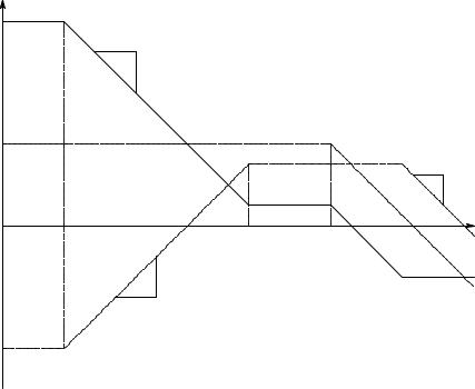
dB |
CMRR |
|
|
|
100 |
|
|
|
|
|
|
|
|
|
|
|
−6 dB/octave |
|
|
40 |
AD(f) |
|
|
|
|
|
|
|
|
3 |
|
|
|
−6 dB/octave |
|
|
|
|
|
10 |
|
|
|
|
|
|
|
|
f |
0 |
f1 |
f2 |
f3 |
f4 |
|
||||
|
|
+6 dB/octave |
|
|
−60 |
AC(f) |
|
|
|
|
|
|
|
FIGURE 3.4
Typical Bode plot asymptotes for the common-mode gain frequency response, the differencemode gain frequency response, and the common-mode rejection ratio frequency response.
in Section 3.5. Figure 3.4 illustrates typical Bode AR asymptote plots for these parameters for a DA. For example, 20 log AD( f ) starts out at +40 dB at dc (gain of 100) and its Bode AR has its first break frequency at f3 Hz. Starting at −60 dB at dc (gain of 0.001), 20 log AC( f ) has a zero at approximately the open-loop amplifier’s break frequency, f1; its Bode AR increases at +20 dB/decade until it reaches a high frequency pole at f2, where it flattens out. Because the numerical CMRR = AD( f ) / AC( f ) , CMRRdB is simply:
CMRRdB = 20 log AD( f ) −20 log AC( f ) |
(3.16) |
Thus, CMRRdB = 100 dB at dc and decreases at −20 dB/decade from f1 to f2, where it levels off at 30 dB. At f3 the CMRRdB again drops off at −20 dB/decade. Good DA design tries to make f1 as large as possible to extend the high CMRR region well into the frequency range of common-mode interference and noise.
© 2004 by CRC Press LLC