

- •Analysis and Application of Analog Electronic Circuits to Biomedical Instrumentation
- •Dedication
- •Preface
- •Reader Background
- •Rationale
- •Description of the Chapters
- •Features
- •The Author
- •Table of Contents
- •1.1 Introduction
- •1.2 Sources of Endogenous Bioelectric Signals
- •1.3 Nerve Action Potentials
- •1.4 Muscle Action Potentials
- •1.4.1 Introduction
- •1.4.2 The Origin of EMGs
- •1.5 The Electrocardiogram
- •1.5.1 Introduction
- •1.6 Other Biopotentials
- •1.6.1 Introduction
- •1.6.2 EEGs
- •1.6.3 Other Body Surface Potentials
- •1.7 Discussion
- •1.8 Electrical Properties of Bioelectrodes
- •1.9 Exogenous Bioelectric Signals
- •1.10 Chapter Summary
- •2.1 Introduction
- •2.2.1 Introduction
- •2.2.4 Schottky Diodes
- •2.3.1 Introduction
- •2.4.1 Introduction
- •2.5.1 Introduction
- •2.5.5 Broadbanding Strategies
- •2.6 Photons, Photodiodes, Photoconductors, LEDs, and Laser Diodes
- •2.6.1 Introduction
- •2.6.2 PIN Photodiodes
- •2.6.3 Avalanche Photodiodes
- •2.6.4 Signal Conditioning Circuits for Photodiodes
- •2.6.5 Photoconductors
- •2.6.6 LEDs
- •2.6.7 Laser Diodes
- •2.7 Chapter Summary
- •Home Problems
- •3.1 Introduction
- •3.2 DA Circuit Architecture
- •3.4 CM and DM Gain of Simple DA Stages at High Frequencies
- •3.4.1 Introduction
- •3.5 Input Resistance of Simple Transistor DAs
- •3.7 How Op Amps Can Be Used To Make DAs for Medical Applications
- •3.7.1 Introduction
- •3.8 Chapter Summary
- •Home Problems
- •4.1 Introduction
- •4.3 Some Effects of Negative Voltage Feedback
- •4.3.1 Reduction of Output Resistance
- •4.3.2 Reduction of Total Harmonic Distortion
- •4.3.4 Decrease in Gain Sensitivity
- •4.4 Effects of Negative Current Feedback
- •4.5 Positive Voltage Feedback
- •4.5.1 Introduction
- •4.6 Chapter Summary
- •Home Problems
- •5.1 Introduction
- •5.2.1 Introduction
- •5.2.2 Bode Plots
- •5.5.1 Introduction
- •5.5.3 The Wien Bridge Oscillator
- •5.6 Chapter Summary
- •Home Problems
- •6.1 Ideal Op Amps
- •6.1.1 Introduction
- •6.1.2 Properties of Ideal OP Amps
- •6.1.3 Some Examples of OP Amp Circuits Analyzed Using IOAs
- •6.2 Practical Op Amps
- •6.2.1 Introduction
- •6.2.2 Functional Categories of Real Op Amps
- •6.3.1 The GBWP of an Inverting Summer
- •6.4.3 Limitations of CFOAs
- •6.5 Voltage Comparators
- •6.5.1 Introduction
- •6.5.2. Applications of Voltage Comparators
- •6.5.3 Discussion
- •6.6 Some Applications of Op Amps in Biomedicine
- •6.6.1 Introduction
- •6.6.2 Analog Integrators and Differentiators
- •6.7 Chapter Summary
- •Home Problems
- •7.1 Introduction
- •7.2 Types of Analog Active Filters
- •7.2.1 Introduction
- •7.2.3 Biquad Active Filters
- •7.2.4 Generalized Impedance Converter AFs
- •7.3 Electronically Tunable AFs
- •7.3.1 Introduction
- •7.3.3 Use of Digitally Controlled Potentiometers To Tune a Sallen and Key LPF
- •7.5 Chapter Summary
- •7.5.1 Active Filters
- •7.5.2 Choice of AF Components
- •Home Problems
- •8.1 Introduction
- •8.2 Instrumentation Amps
- •8.3 Medical Isolation Amps
- •8.3.1 Introduction
- •8.3.3 A Prototype Magnetic IsoA
- •8.4.1 Introduction
- •8.6 Chapter Summary
- •9.1 Introduction
- •9.2 Descriptors of Random Noise in Biomedical Measurement Systems
- •9.2.1 Introduction
- •9.2.2 The Probability Density Function
- •9.2.3 The Power Density Spectrum
- •9.2.4 Sources of Random Noise in Signal Conditioning Systems
- •9.2.4.1 Noise from Resistors
- •9.2.4.3 Noise in JFETs
- •9.2.4.4 Noise in BJTs
- •9.3 Propagation of Noise through LTI Filters
- •9.4.2 Spot Noise Factor and Figure
- •9.5.1 Introduction
- •9.6.1 Introduction
- •9.7 Effect of Feedback on Noise
- •9.7.1 Introduction
- •9.8.1 Introduction
- •9.8.2 Calculation of the Minimum Resolvable AC Input Voltage to a Noisy Op Amp
- •9.8.5.1 Introduction
- •9.8.5.2 Bridge Sensitivity Calculations
- •9.8.7.1 Introduction
- •9.8.7.2 Analysis of SNR Improvement by Averaging
- •9.8.7.3 Discussion
- •9.10.1 Introduction
- •9.11 Chapter Summary
- •Home Problems
- •10.1 Introduction
- •10.2 Aliasing and the Sampling Theorem
- •10.2.1 Introduction
- •10.2.2 The Sampling Theorem
- •10.3 Digital-to-Analog Converters (DACs)
- •10.3.1 Introduction
- •10.3.2 DAC Designs
- •10.3.3 Static and Dynamic Characteristics of DACs
- •10.4 Hold Circuits
- •10.5 Analog-to-Digital Converters (ADCs)
- •10.5.1 Introduction
- •10.5.2 The Tracking (Servo) ADC
- •10.5.3 The Successive Approximation ADC
- •10.5.4 Integrating Converters
- •10.5.5 Flash Converters
- •10.6 Quantization Noise
- •10.7 Chapter Summary
- •Home Problems
- •11.1 Introduction
- •11.2 Modulation of a Sinusoidal Carrier Viewed in the Frequency Domain
- •11.3 Implementation of AM
- •11.3.1 Introduction
- •11.3.2 Some Amplitude Modulation Circuits
- •11.4 Generation of Phase and Frequency Modulation
- •11.4.1 Introduction
- •11.4.3 Integral Pulse Frequency Modulation as a Means of Frequency Modulation
- •11.5 Demodulation of Modulated Sinusoidal Carriers
- •11.5.1 Introduction
- •11.5.2 Detection of AM
- •11.5.3 Detection of FM Signals
- •11.5.4 Demodulation of DSBSCM Signals
- •11.6 Modulation and Demodulation of Digital Carriers
- •11.6.1 Introduction
- •11.6.2 Delta Modulation
- •11.7 Chapter Summary
- •Home Problems
- •12.1 Introduction
- •12.2.1 Introduction
- •12.2.2 The Analog Multiplier/LPF PSR
- •12.2.3 The Switched Op Amp PSR
- •12.2.4 The Chopper PSR
- •12.2.5 The Balanced Diode Bridge PSR
- •12.3 Phase Detectors
- •12.3.1 Introduction
- •12.3.2 The Analog Multiplier Phase Detector
- •12.3.3 Digital Phase Detectors
- •12.4 Voltage and Current-Controlled Oscillators
- •12.4.1 Introduction
- •12.4.2 An Analog VCO
- •12.4.3 Switched Integrating Capacitor VCOs
- •12.4.6 Summary
- •12.5 Phase-Locked Loops
- •12.5.1 Introduction
- •12.5.2 PLL Components
- •12.5.3 PLL Applications in Biomedicine
- •12.5.4 Discussion
- •12.6 True RMS Converters
- •12.6.1 Introduction
- •12.6.2 True RMS Circuits
- •12.7 IC Thermometers
- •12.7.1 Introduction
- •12.7.2 IC Temperature Transducers
- •12.8 Instrumentation Systems
- •12.8.1 Introduction
- •12.8.5 Respiratory Acoustic Impedance Measurement System
- •12.9 Chapter Summary
- •References

256 |
Analysis and Application of Analog Electronic Circuits |
vi
|
|
vo |
|
HI |
vo |
− |
0 |
(vi − vi’) |
|
vi’
FIGURE 6.8
Block diagram of an ideal comparator I/O characteristic.
6.5Voltage Comparators
6.5.1Introduction
The integrated circuit analog voltage comparator (VC) is a useful circuit element with many applications in biomedical instrumentation. The VC is a simple analog/digital interface element; its input is an analog voltage difference and its output is logic HI or LO. An ideal VC performs the operation shown in Figure 6.8. That is, its output is logic HI when (vi − vi′) > 0 and LO when (vi − vi′) ≤ 0. vi or vi′ can be a dc reference voltage, φ.
An actual VC circuit combines the front end of an analog differential amplifier (see Chapter 3) with the output stage of an open-collector logic gate. The differential front end can be described in terms of: difference-mode gain; common-mode gain; common-mode rejection ratio; slew rate; and dc input offset voltage. Figure 6.9 illustrates the output stage of the well-known LM311 VC. Note that the analog DA front end has a symmetrical push–pull output coupled to the driving transistors, Q8 and Q9, of the output stage. To heuristically examine how this circuit works, assume that (vi − vi′) > 0. Assuming a large DM gain for the DA, vo′ goes negative, turning off Q8 and allowing vb10 to go positive. Positive-going vb10 makes vb11 go positive, turning off Q11. When Q11 turns off, it turns off Q15, allowing Vo at its collector to go toward VLL (+5 V) or logic HI. Also, (vi − vi′) > 0 causes vo to go positive, causing Q9 to turn on. The Q9 emitter goes positive, forcing the Q8 emitter to go positive and further turning it off, etc.
All this action is summarized in Figure 6.10. vi′ is the dc reference voltage, Vφ. Note that the static transfer curve of the comparator in Figure 6.10 shows a narrow range of finite differential voltage gain (e.g., 2 ∞ 105 for the AD CMP04). Note that some VCs also have complementary (Q) outputs for design versatility (e.g., the AD9696 TTL output VC).
A wide range of comparator switching speeds are available, given a step change in the polarity of (vi − vi′). VC switching speed has two components:
(1) a pure delay time between the input step change and the beginning of output state change and (2) the time it takes for Vo to swing from LO to HI
© 2004 by CRC Press LLC

Operational Amplifiers |
257 |
VCC (+15 V)
|
750 Ω |
|
600 Ω |
VLL (+5 V) |
|
vb10 |
Q10 |
|
|
|
v2’ |
|
|
|
vi’ |
Q8 |
|
|
1 kΩ Rc |
|
DA |
|
ve11 |
|
|
|
|
||
|
|
|
|
|
vi |
|
Q9 |
|
Vo |
|
v2 |
vb11 |
Q11 |
|
|
|
|
|
Q15 |
|
|
|
|
600 Ω |
|
500 µA |
I10 |
Q16 |
4 Ω |
|
|
|
|
|
Logic gnd.
VEE (−15 V)
FIGURE 6.9
Partial (output circuit) schematic of an LM311 analog comparator. Note that an analog DA stage output is converted to an open-collector TTL output BJT.
|
VLL (+5 V) |
Vs |
Rc |
|
|
VC |
Vo |
|
Q15 |
Vφ
|
Vo |
|
5 V |
VLL |
|
|
Q15 ON |
Q15 OFF |
|
|
KD |
0.2 |
|
Vs |
|
0 |
Vφ |
FIGURE 6.10
Top: analog comaparator. Bottom: transfer characteristic of the comparator. Comparator gain, KD, in the linear region is as high as an op amp.
© 2004 by CRC Press LLC

258 |
Analysis and Application of Analog Electronic Circuits |
RF
R1 vi
Vo
VC
vi’
Vs
VR
 Vo
Vo
HI
VH
LO |
Vs |
0
VsLO VsHI
FIGURE 6.11
Top: a voltage comparator connected to have hysteresis; note PFB. Bottom: dimensions of the hysteresis I/O characteristic.
(or HI to LO). This latter delay is limited by the VC slew rate. The total time for a comparator to reach its new output state following an input step change in (vi − vi′) polarity is called the propagation delay time, tPD.
The LM311 comparator output changes state about 200 ns following the input step change. Newer designs such as the AD790 change states in approximately 40 ns. The AD790 also claims a maximum offset voltage magnitude of 250 μV. The AD96685 VC claims a 2.5-ns propagation delay and has a whopping 1 mV Vos . Unlike the LM311, most comparators do not have a means of nulling their VOS.
The input impedance of VCs is generally fairly high, about what one might expect from a fast BJT-input op amp. For example, the AD790 VC has an input impedance given as 20 megohms in parallel with 2 pF to ground. VC output impedance depends on the output state; if Vo is LO, the open-collector output transistor is saturated and Ro is in the tens of ohms. If Vo is HI, then the output transistor is cut off and Ro is basically the external pull-up resistance used with the comparator. (Some VCs put this resistor in the IC.)
VCs are often operated with hysteresis to give them noise immunity. Figure 6.11 illustrates an external positive feedback circuit that gives hysteresis, and the ideal static I/O curve for the circuit. To find an expression for the exact input voltages at which the VC’s output changes state, write a node equation on the noninverting vi node:
© 2004 by CRC Press LLC

Operational Amplifiers |
259 |
Vi [G1 + GF] − Vs G1 − VoLO GF = 0 |
(6.56) |
At switching LO HI, Vi is assumed to equal Vi. = VREF. Thus, from the preceding equation,
VsHI |
= |
VR (G1 + GF )− VoLOGF |
= VR (1+ R1 RF )− VoLO (RL RF ) |
(6.57) |
|
||||
|
|
G1 |
|
|
When Vs > VsHI, Vo = VoHI = + 5 V. Now Vs must decrease to VsLO before Vo = VoLO = 0.2 V again.
Calculation of VsLO uses the preceding approach, except that VoHI is used in Equation 6.57:
VsLO = VR (1+ R1 RF )− VoHI (R1 RF ) |
(6.58) |
Consider a numerical example: let R1 = 10 kΩ; RF = 100 kΩ; VR = +1.0 V;
VoHI = +5.0 V; and VoLO = +0.2 V. From these values: VsHI = 1.08 V and VsLO = 0.60 V; the width of the hysteresis can easily be shown to be:
VH = (VoHI − VoLO )(R1 RF ) = 0.48 V. |
(6.59) |
Note that the feedback around the comparator is PVF (see Chapter 4). Not only does the VC with PFV have hysteresis for noise immunity, but the VC with hysteresis can also be used as a simple limit-cycling ON–OFF controller for a switched control system such as an oven heater (Franco, 1988, Chapter 7). It is also possible to reverse the positions of the dc reference voltage, VR, and the input signal, Vs, in Figure 6.11 and still have hysteresis.
It is left as an exercise for the reader to find expressions for VsLO, VsHI, and VH under these conditions.
6.5.2. Applications of Voltage Comparators
Comparators find many applications in biomedical engineering. They are used in bar-graph (LED) display meters; flash ADC converters (see Section 10.5.5); overand under-range alarms; static window circuits; ON–OFF controllers; and dynamic pulse-height discriminators used in nuclear medicine and neurophysiology. The first example examines a simple battery overvoltage alarm used to indicate that charging should cease. This circuit is shown
in Figure 6.12. When VBatt > VREF, the output (open collector) transistor (Q15) in the VC is turned off, allowing the base of Q1 to conduct through the 1-kΩ
pull-up resistor, saturating Q1. The current through the lit LED is approximately (5 − 0.2 − 1.5)/330 = 10 mA. If VBatt < VREF, Q15 is ON and saturated,
© 2004 by CRC Press LLC
260 |
Analysis and Application of Analog Electronic Circuits |
VLL (+5 V)
1 kΩ 330Ω
|
LED |
|
hν |
VBatt |
|
VC |
Q1 |
Q15 |
VREF
FIGURE 6.12
A comparator circuit that will light an LED when VBatt > VREF. If VBatt < VREF, then Q15 of the comparator is on and saturated, pulling Q1’s base low and turning it and the LED off.
VLL (+5 V)
1 kΩ 330Ω
VφHI |
|
|
|
|
|
|
|
VC |
|
|
|
|
|
|
|
Q15H |
IC |
|
IC |
|
LED ON |
|
|
|
|
|
|
|
|
||
|
|
|
|
|
|
|
|
Vs |
|
Q1 |
Q15L ON, |
Q15H & Q15L OFF |
Q15L OFF, |
||
|
Q15H |
OFF |
|
|
Q15H ON |
||
|
|
|
|
|
|||
VC |
|
|
LED OFF |
|
|
LED OFF Vs |
|
|
|
|
|
|
|
|
|
Q15L |
|
|
0 |
|
VφLO |
VφHI |
|
|
|
|
|
|
|
|
|
VφLO |
|
|
|
|
|
|
|
FIGURE 6.13
A comparator voltage range window that turns the LED on when Vs lies between VφLO and VφHI .
pulling the base of Q1 down to approximately 0.2 V, keeping it off and the LED unlit.
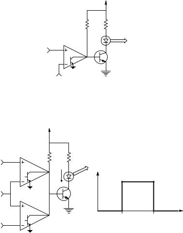
The second example of the use of VCs is a static window comparator circuit that lights an LED while the input voltage falls in a certain range, or window, of values. The circuit is shown in Figure 6.13. Note that tying the two open collector output transistors together to a common pull-up resistor effectively makes an AND gate. Both comparator outputs must be HI (Q15L AND Q15H are cut off) to light the LED. If either Q15 is ON, the base of Q1 is pulled
down to that Q15’s Vcsat and Q1 is cut off.
In a third and final example of using VCs, examine a simple nerve spike pulse-height discriminator designed by the author. This circuit is designed to be used in neurophysiological recording; it selects only those nerve
© 2004 by CRC Press LLC