

- •Analysis and Application of Analog Electronic Circuits to Biomedical Instrumentation
- •Dedication
- •Preface
- •Reader Background
- •Rationale
- •Description of the Chapters
- •Features
- •The Author
- •Table of Contents
- •1.1 Introduction
- •1.2 Sources of Endogenous Bioelectric Signals
- •1.3 Nerve Action Potentials
- •1.4 Muscle Action Potentials
- •1.4.1 Introduction
- •1.4.2 The Origin of EMGs
- •1.5 The Electrocardiogram
- •1.5.1 Introduction
- •1.6 Other Biopotentials
- •1.6.1 Introduction
- •1.6.2 EEGs
- •1.6.3 Other Body Surface Potentials
- •1.7 Discussion
- •1.8 Electrical Properties of Bioelectrodes
- •1.9 Exogenous Bioelectric Signals
- •1.10 Chapter Summary
- •2.1 Introduction
- •2.2.1 Introduction
- •2.2.4 Schottky Diodes
- •2.3.1 Introduction
- •2.4.1 Introduction
- •2.5.1 Introduction
- •2.5.5 Broadbanding Strategies
- •2.6 Photons, Photodiodes, Photoconductors, LEDs, and Laser Diodes
- •2.6.1 Introduction
- •2.6.2 PIN Photodiodes
- •2.6.3 Avalanche Photodiodes
- •2.6.4 Signal Conditioning Circuits for Photodiodes
- •2.6.5 Photoconductors
- •2.6.6 LEDs
- •2.6.7 Laser Diodes
- •2.7 Chapter Summary
- •Home Problems
- •3.1 Introduction
- •3.2 DA Circuit Architecture
- •3.4 CM and DM Gain of Simple DA Stages at High Frequencies
- •3.4.1 Introduction
- •3.5 Input Resistance of Simple Transistor DAs
- •3.7 How Op Amps Can Be Used To Make DAs for Medical Applications
- •3.7.1 Introduction
- •3.8 Chapter Summary
- •Home Problems
- •4.1 Introduction
- •4.3 Some Effects of Negative Voltage Feedback
- •4.3.1 Reduction of Output Resistance
- •4.3.2 Reduction of Total Harmonic Distortion
- •4.3.4 Decrease in Gain Sensitivity
- •4.4 Effects of Negative Current Feedback
- •4.5 Positive Voltage Feedback
- •4.5.1 Introduction
- •4.6 Chapter Summary
- •Home Problems
- •5.1 Introduction
- •5.2.1 Introduction
- •5.2.2 Bode Plots
- •5.5.1 Introduction
- •5.5.3 The Wien Bridge Oscillator
- •5.6 Chapter Summary
- •Home Problems
- •6.1 Ideal Op Amps
- •6.1.1 Introduction
- •6.1.2 Properties of Ideal OP Amps
- •6.1.3 Some Examples of OP Amp Circuits Analyzed Using IOAs
- •6.2 Practical Op Amps
- •6.2.1 Introduction
- •6.2.2 Functional Categories of Real Op Amps
- •6.3.1 The GBWP of an Inverting Summer
- •6.4.3 Limitations of CFOAs
- •6.5 Voltage Comparators
- •6.5.1 Introduction
- •6.5.2. Applications of Voltage Comparators
- •6.5.3 Discussion
- •6.6 Some Applications of Op Amps in Biomedicine
- •6.6.1 Introduction
- •6.6.2 Analog Integrators and Differentiators
- •6.7 Chapter Summary
- •Home Problems
- •7.1 Introduction
- •7.2 Types of Analog Active Filters
- •7.2.1 Introduction
- •7.2.3 Biquad Active Filters
- •7.2.4 Generalized Impedance Converter AFs
- •7.3 Electronically Tunable AFs
- •7.3.1 Introduction
- •7.3.3 Use of Digitally Controlled Potentiometers To Tune a Sallen and Key LPF
- •7.5 Chapter Summary
- •7.5.1 Active Filters
- •7.5.2 Choice of AF Components
- •Home Problems
- •8.1 Introduction
- •8.2 Instrumentation Amps
- •8.3 Medical Isolation Amps
- •8.3.1 Introduction
- •8.3.3 A Prototype Magnetic IsoA
- •8.4.1 Introduction
- •8.6 Chapter Summary
- •9.1 Introduction
- •9.2 Descriptors of Random Noise in Biomedical Measurement Systems
- •9.2.1 Introduction
- •9.2.2 The Probability Density Function
- •9.2.3 The Power Density Spectrum
- •9.2.4 Sources of Random Noise in Signal Conditioning Systems
- •9.2.4.1 Noise from Resistors
- •9.2.4.3 Noise in JFETs
- •9.2.4.4 Noise in BJTs
- •9.3 Propagation of Noise through LTI Filters
- •9.4.2 Spot Noise Factor and Figure
- •9.5.1 Introduction
- •9.6.1 Introduction
- •9.7 Effect of Feedback on Noise
- •9.7.1 Introduction
- •9.8.1 Introduction
- •9.8.2 Calculation of the Minimum Resolvable AC Input Voltage to a Noisy Op Amp
- •9.8.5.1 Introduction
- •9.8.5.2 Bridge Sensitivity Calculations
- •9.8.7.1 Introduction
- •9.8.7.2 Analysis of SNR Improvement by Averaging
- •9.8.7.3 Discussion
- •9.10.1 Introduction
- •9.11 Chapter Summary
- •Home Problems
- •10.1 Introduction
- •10.2 Aliasing and the Sampling Theorem
- •10.2.1 Introduction
- •10.2.2 The Sampling Theorem
- •10.3 Digital-to-Analog Converters (DACs)
- •10.3.1 Introduction
- •10.3.2 DAC Designs
- •10.3.3 Static and Dynamic Characteristics of DACs
- •10.4 Hold Circuits
- •10.5 Analog-to-Digital Converters (ADCs)
- •10.5.1 Introduction
- •10.5.2 The Tracking (Servo) ADC
- •10.5.3 The Successive Approximation ADC
- •10.5.4 Integrating Converters
- •10.5.5 Flash Converters
- •10.6 Quantization Noise
- •10.7 Chapter Summary
- •Home Problems
- •11.1 Introduction
- •11.2 Modulation of a Sinusoidal Carrier Viewed in the Frequency Domain
- •11.3 Implementation of AM
- •11.3.1 Introduction
- •11.3.2 Some Amplitude Modulation Circuits
- •11.4 Generation of Phase and Frequency Modulation
- •11.4.1 Introduction
- •11.4.3 Integral Pulse Frequency Modulation as a Means of Frequency Modulation
- •11.5 Demodulation of Modulated Sinusoidal Carriers
- •11.5.1 Introduction
- •11.5.2 Detection of AM
- •11.5.3 Detection of FM Signals
- •11.5.4 Demodulation of DSBSCM Signals
- •11.6 Modulation and Demodulation of Digital Carriers
- •11.6.1 Introduction
- •11.6.2 Delta Modulation
- •11.7 Chapter Summary
- •Home Problems
- •12.1 Introduction
- •12.2.1 Introduction
- •12.2.2 The Analog Multiplier/LPF PSR
- •12.2.3 The Switched Op Amp PSR
- •12.2.4 The Chopper PSR
- •12.2.5 The Balanced Diode Bridge PSR
- •12.3 Phase Detectors
- •12.3.1 Introduction
- •12.3.2 The Analog Multiplier Phase Detector
- •12.3.3 Digital Phase Detectors
- •12.4 Voltage and Current-Controlled Oscillators
- •12.4.1 Introduction
- •12.4.2 An Analog VCO
- •12.4.3 Switched Integrating Capacitor VCOs
- •12.4.6 Summary
- •12.5 Phase-Locked Loops
- •12.5.1 Introduction
- •12.5.2 PLL Components
- •12.5.3 PLL Applications in Biomedicine
- •12.5.4 Discussion
- •12.6 True RMS Converters
- •12.6.1 Introduction
- •12.6.2 True RMS Circuits
- •12.7 IC Thermometers
- •12.7.1 Introduction
- •12.7.2 IC Temperature Transducers
- •12.8 Instrumentation Systems
- •12.8.1 Introduction
- •12.8.5 Respiratory Acoustic Impedance Measurement System
- •12.9 Chapter Summary
- •References

502 |
Analysis and Application of Analog Electronic Circuits |
|
|
KpKv = 1 (2τ) |
(12.60) |
Also, from the RL geometry, ωn = 2 (2τ). The loop filter time constant is found by substituting Equation 12.60 for Kp Kv into Equation 12.58 and solving the resultant quadratic equation for τ2, and thus τ.
ωc = KpKv |
|
1 τ |
(12.61) |
|||
|
ω |
2 |
+ 1 τ2 |
|
||
|
|
|
c |
|
|
|
¬ |
|
|
|
|
|
|
τ4 + τ2 ωc2 − 1 |
(4 |
|
ωc4 ) = 0 |
(12.62) |
||
When Δωc = 2π(8.8) = 55.292 r/s is substituted into Equation 12.62, τ = 8.231 ∞ 10−3 sec, ωn = 85.91 r/s, and Kp Kv = KT = 60.75 r/s.
The NE/SE567 tone decoder PLL IC (Philips Semiconductors’ linear products) data sheets contain a wealth of design and operating information in graphical form, including the greatest number of input cycles in a tone burst before the PLL acquires the input and goes high. Tone decoders are used in emergency response radios (for EMTs, firemen) to gate transmission of alert messages.
12.5.4Discussion
PLLs are versatile systems with wide applications in communications, control, and instrumentation; this section has only scratched the surface of this topic. The interested reader is encouraged to examine the many texts dealing with the design and applications of this ubiquitous IC. See, for example, Northrop (1990, Chapter 11); Gray and Meyer (1984, Chapter 10); Blanchard (1976); Exar Integrated Systems (1979); and Grebene (1971).
12.6 True RMS Converters
12.6.1Introduction
The analog true RMS converter is a system that provides a dc output proportional to the root-mean-square of the input signal, v(t). An analog RMS operation first squares v1(t) then estimates the mean value of v2(t), generally by time averaging by low-pass filtering. Finally, the square root of the mean squared value, v2 (t) , is taken.
The RMS value of a sine wave is easily seen to be its peak value divided by the 2. When one says that the U.S. residential line voltage is 120V, this
© 2004 by CRC Press LLC
Examples of Special Analog Circuits and Systems |
503 |
means RMS volts. The average power dissipated in a resistor, R, that has a sinusoidal voltage across it is Pav = (VRMS)2 R watts. Random signals and noise can also be described by their mean-squared values or RMS values. In fact, noise voltages are characterized by measuring them with a true RMS voltmeter; it is meaningless to measure random noise with a rectifier-type ac meter.
12.6.2True RMS Circuits
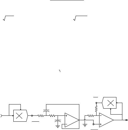
Figure 12.30 illustrates the block diagram of an explicit RMS system using analog multipliers and op amp ICs. The low-pass filter (LPF) is a quadratic Sallen and Key design. Its transfer function is:
1 |
|
H(s) = s2 ωn2 + s(2ξ) ωn + 1 |
(12.63) |
Its undamped natural frequency can be shown to be (Northrop, 1997) ωn = 1/(R C1C2) r/s and its damping factor is ξ = (C2C1 ). The low-pass filtering action effectively estimates the mean of v12(t)/10. The output, Vo, can be found by assuming the third op amp is ideal and writing the node equation for its summing junction:
|
|
|
|
|
|
|
|
|
v 2 |
(t) |
= |
|
V 2 |
|
|
1 |
|
|
|
o |
(12.64) |
||
|
10 R |
|
10 R |
||||
|
|
|
|
||||
Thus, |
|
|
|
|
|
|
|
|
V = |
v 2 |
(t), |
(12.65) |
|||
|
o |
|
|
1 |
|
|
|
the RMS value of v1(t). Note that this analog square root circuit requires that v12(t) ≥ 0 and it is.
|
|
|
Vo2 |
AM |
|
|
|
10 |
|
|
|
C1 |
|
R |
|
|
|
|
|
|
R |
R |
R |
|
v1(t) |
|
|
|
Vo |
|
v12(t) |
|
|
|
|
C2 |
|
|
|
AM |
10 |
|
|
|
|
|
|
||
|
|
____ |
|
|
|
|
|
|
|
|
|
|
v12(t) |
|
|
|
S&K LPF |
10 |
|
FIGURE 12.30
An analog circuit that finds the true RMS value of the input voltage, v1(t). Two analog multipliers (AM) are used.
© 2004 by CRC Press LLC

504 |
Analysis and Application of Analog Electronic Circuits |
|
|
MFC |
|
Vo |
|
|
VY |
|
|
||
V1 |
|
VY(VZ /Vx )m |
V12 /Vo |
R Vo |
|
|
|||||
|
|
||||
|
|
m = 1 |
(×1 Buffer) |
||
|
|
||||
|
VZ |
|
|
||
|
VX |
|
C |
||
|
|
|
|
||
|
|
|
|
|
|
|
|
|
|
|
|
FIGURE 12.31
A true RMS conversion circuit using a multifunction converter.
Another (implicit) TRMS circuit can be made from an analog IC known as a multifunction converter (MFC). The MFC, such as the Burr–Brown 4302, computes the analog function,
V2 = VY (VZ VX )m, 5 ≥ m ≥ 1, 0 ≤ (Vx , Vy , VZ )≤ 10 V |
(12.66) |
From the circuit of Figure 12.31, note that the R–C LPF acts as an averager of V2 = V12 Vo. Thus, the identity:
|
|
|
|
V = V2 |
V |
(12.67) |
|
o 1 |
o |
|
|
can be written and, from this, it is clear that
|
|
|
|
|
V2 |
= V2 |
MSV, |
(12.68) |
|
o |
1 |
|
|
|
and Vo is the RMS value of V1.
The RMS voltage of a signal can also be found using vacuum thermocouple (VTC) elements, as shown in Figure 12.32. The vacuum thermocouple consists of a thin heater wire of resistance RHo at a reference temperature, TA (e.g., 25ºC), inside an evacuated glass envelope. Electrically insulated from but thermally intimate with RH is a thermocouple junction (TJ) (Pallàs–Areny and Webster, 2001; Northrop, 1997; Lion, 1959). For example, the venerable Western Electric model 20D VTC has RH = 35 Ω at room temperature; the nominal thermocouple resistance (Fe and constantan wires) is 12 Ω. The maximum heater current is 16 mA RMS (exceed this and the heater melts). The 20D VTC has an open-circuit DC output voltage Vo = 0.005 V when IH = 0.007 A RMS. Because the heater temperature is proportional to the average power dissipated in the heater, or the mean squared current ∞ RH, this VTC produces KT = 0.005/[(0.007)2 ∞ 35] = 2.915 V/W, or mV/mW. The EMF of the tesla joules is given in general by the truncated power series:
V = A( T) + B( T)2 |
2 + C( T)3 3 S T |
(12.69) |
J |
|
|
© 2004 by CRC Press LLC

Examples of Special Analog Circuits and Systems |
505 |
|
VCCS |
|
|
|
|
|
|
v1(t) |
i1(t) |
VTC1 |
B |
+VA |
− |
Cu |
|
Gm |
|
+ |
|
|
|
VD |
|
|
|
|
|
|
TA |
DA |
|
|
|
RH |
Vm |
+VB |
|
||
|
|
− |
Cu |
|
|||
|
|
TM |
− A |
|
|
|
|
TA
VTC2
− A
RH |
VF |
B |
|
TF |
+ |
|
C |
|
|
|
|
IF (DC) |
VCCS |
|
R |
|
|
||
|
|
Vo |
VD |
|
Gm |
|
OA |
+Vlim −Vlim
FIGURE 12.32
A feedback vacuum thermocouple true RMS voltmeter (or ammeter).
where T is the difference in junction temperature above the ambient temperature, TA. S for an iron/constantan (Fe/CN) TC = 50 ∞ 10−6. In a VTC, T = TH − TA. TH is the heater resistor temperature as the result of Joule’s
law heating. T can be modeled by:
|
|
|
|
|
|
T = i 2 |
R |
H |
Θ |
(12.70) |
|
|
h |
|
|
|
|
The electrical power dissipated in the heater element is given by the meansquared current in the heater times the heater resistance. The thermal resistance of the heater in vacuo is Θ; its units are degrees Celsius/watt. This relation is not that simple because RH increases with increasing temperature — an effect that can be approximated by:
RH = RHo (1 + αΔT) |
(12.71) |
where α is the alpha tempco of the RH resistance wire. If the preceding
equation is substituted into Equation 12.70, one can solve for |
T: |
||||||||||
|
|
|
|
Θ |
|
|
|
|
|
|
|
|
|
i 2 |
R |
|
|
|
|
|
|||
|
|
|
2 |
2 |
|
|
|||||
1 |
Ho |
|
|
|
|
|
|||||
T = |
1− α[i12 RHo Θ] |
i1 |
RHo Θ[1+ α i1 RHo Θ] |
(12.72) |
|||||||
Assuming that RH remains constant, |
|
T = VJ S = 0.005/(50 ∞ 10−6) = 100ºC |
|||||||||
from Equation 12.69. The thermal resistance of the WE 20D VTC is thus Θ = T/PH = 100∞ (1.715 ∞ 10−3) W = 5.831 ∞ 104 ºC/W. This thermal resistance
is large because of the vacuum. High Θ gives increased VTC sensitivity.
© 2004 by CRC Press LLC

506 |
Analysis and Application of Analog Electronic Circuits |
|
|
|
|
|
(Divider = log subtractor) |
||||
|
|
(Absval) |
(log squarer) |
|
|
|
(antilog) |
||
v1(t) |
|
* |
v1(t) |
log[ v1(t) 2] |
+ |
|
V2 |
10kV2 |
v12(t)/ Vo |
|
|
= 2 log[v1(t)] |
|
− |
|
||||
|
|
|
|
|
|
|
|||
|
|
|
|
|
|
|
|
||
V2 = |
2 log[v1(t)] − log(Vo) |
(log) |
|
|
Vo |
|
|
log(Vo) |
|
|
____ |
(LPF) |
Vo = v12(t)/ Vo |
|
|
|
____ |
|
Vo = |
√ v1(t)2 |
|
|
(DC) |
FIGURE 12.33
Simplified block diagram of Analog Devices’ AD637 true analog RMS conversion IC.
In the feedback TRMS meter, the TC EMF is found by substituting Equation 12.72 into Equation 12.69. Examination of the TRMS TC feedback voltmeter of Figure 12.32 shows that it is a self-nulling system. At equilibrium, VF = Vm and it can be shown from the thermoelectric laws that VA – VB = 0, so VD = 0. VF and Vm are given approximately by:
|
|
RHo Θ]= Vm |
|
|
|
|
˘ |
|
2 |
2 |
|
2 |
RHo |
(12.73) |
|||
VF A[IF |
RHo Θ]= A[(VoGm ) |
A (v1 |
(t)Gm ) |
Θ˙ |
||||
|
|
|
|
|
|
˚ |
|
|
From this equation, it can be written that
Vo (DC) = [ |
|
] |
|
v12 (t) |
(12.74) |
i.e., Vo equals the RMS value of v1(t).
Note that this system is an even-error system. That is, the voltage VF is independent of the sign of Vo because the same heating occurs regardless of the sign of IF in RH. Not shown but necessary to the operation of this system is a means of initially setting Vo 0 just before the measurement is made. Then Vo and IF increase until VD 0 and Vm = VF.
Still another class of true RMS to DC converters is found in the Analog Devices’ AD536A/636 and AD637 ICs. Figure 12.33 illustrates the block diagram of the AD637 TRMS converter IC. The front end of this system makes use of the identity:
v 2 |
= |
|
v |
|
2 |
≥ 0 |
(12.75) |
|
|
||||||
1 |
|
|
1 |
|
|
|
|
Squaring is done by taking the logarithm of v1 and doubling it. Division by Vo is accomplished by subtracting the log of the dc output voltage, Vo, from 2 log(v1), giving V2, which is antilogged to recover v12(t) Vo. v12(t) Vo is low-pass filtered to produce the implicitly derived DC RMS output voltage from v1(t). Figure 12.34 illustrates the organization of the TRMS subsystems
© 2004 by CRC Press LLC
Examples of Special Analog Circuits and Systems |
507 |
1 |
|
14 |
v1(t) |
Abs. Val. |
+Vcc |
NC |
|
NC |
|
Squarer |
|
|
Divider |
|
−Vcc |
|
NC |
CAV |
|
|
+Vcc |
|
NC |
Current
mirror
dB
Vo
|
R |
|
R |
7 |
8 |
OA
Sallen & Key
2-pole LPF
|
R |
C2 |
C3 |
|
FIGURE 12.34
Block diagram of functions on the AD536 true RMS converter chip.
in the AD536 TRMS converter. A two-pole, Sallen and Key low-pass filter is used to give a smooth DC output in this configuration (Kitchin and Counts, 1983).
Note that all true RMS converters estimate the mean of the squared voltage by low-pass filtering. This means that they work well for DC inputs and for inputs whose power density spectra have harmonics well above the break frequency of the LPF. Low-frequency input signals will give ripple on Vo, making TRMS measurement difficult. The size of the LPF time constant is a compromise between meter settling time and the lowest input frequency that can be accurately measured.
Although this text has concentrated on analog electronic systems and ICs in describing TRMS conversion, the reader will appreciate that the entire process can be done digitally, beginning with analog anti-aliasing filtering followed by periodic A-to-D conversion of the signal under consideration. A finite number of samples (a data epoch) are stored in an array. Next, the converted signal is squared, sample by sample, and the results stored in a
© 2004 by CRC Press LLC