

- •Analysis and Application of Analog Electronic Circuits to Biomedical Instrumentation
- •Dedication
- •Preface
- •Reader Background
- •Rationale
- •Description of the Chapters
- •Features
- •The Author
- •Table of Contents
- •1.1 Introduction
- •1.2 Sources of Endogenous Bioelectric Signals
- •1.3 Nerve Action Potentials
- •1.4 Muscle Action Potentials
- •1.4.1 Introduction
- •1.4.2 The Origin of EMGs
- •1.5 The Electrocardiogram
- •1.5.1 Introduction
- •1.6 Other Biopotentials
- •1.6.1 Introduction
- •1.6.2 EEGs
- •1.6.3 Other Body Surface Potentials
- •1.7 Discussion
- •1.8 Electrical Properties of Bioelectrodes
- •1.9 Exogenous Bioelectric Signals
- •1.10 Chapter Summary
- •2.1 Introduction
- •2.2.1 Introduction
- •2.2.4 Schottky Diodes
- •2.3.1 Introduction
- •2.4.1 Introduction
- •2.5.1 Introduction
- •2.5.5 Broadbanding Strategies
- •2.6 Photons, Photodiodes, Photoconductors, LEDs, and Laser Diodes
- •2.6.1 Introduction
- •2.6.2 PIN Photodiodes
- •2.6.3 Avalanche Photodiodes
- •2.6.4 Signal Conditioning Circuits for Photodiodes
- •2.6.5 Photoconductors
- •2.6.6 LEDs
- •2.6.7 Laser Diodes
- •2.7 Chapter Summary
- •Home Problems
- •3.1 Introduction
- •3.2 DA Circuit Architecture
- •3.4 CM and DM Gain of Simple DA Stages at High Frequencies
- •3.4.1 Introduction
- •3.5 Input Resistance of Simple Transistor DAs
- •3.7 How Op Amps Can Be Used To Make DAs for Medical Applications
- •3.7.1 Introduction
- •3.8 Chapter Summary
- •Home Problems
- •4.1 Introduction
- •4.3 Some Effects of Negative Voltage Feedback
- •4.3.1 Reduction of Output Resistance
- •4.3.2 Reduction of Total Harmonic Distortion
- •4.3.4 Decrease in Gain Sensitivity
- •4.4 Effects of Negative Current Feedback
- •4.5 Positive Voltage Feedback
- •4.5.1 Introduction
- •4.6 Chapter Summary
- •Home Problems
- •5.1 Introduction
- •5.2.1 Introduction
- •5.2.2 Bode Plots
- •5.5.1 Introduction
- •5.5.3 The Wien Bridge Oscillator
- •5.6 Chapter Summary
- •Home Problems
- •6.1 Ideal Op Amps
- •6.1.1 Introduction
- •6.1.2 Properties of Ideal OP Amps
- •6.1.3 Some Examples of OP Amp Circuits Analyzed Using IOAs
- •6.2 Practical Op Amps
- •6.2.1 Introduction
- •6.2.2 Functional Categories of Real Op Amps
- •6.3.1 The GBWP of an Inverting Summer
- •6.4.3 Limitations of CFOAs
- •6.5 Voltage Comparators
- •6.5.1 Introduction
- •6.5.2. Applications of Voltage Comparators
- •6.5.3 Discussion
- •6.6 Some Applications of Op Amps in Biomedicine
- •6.6.1 Introduction
- •6.6.2 Analog Integrators and Differentiators
- •6.7 Chapter Summary
- •Home Problems
- •7.1 Introduction
- •7.2 Types of Analog Active Filters
- •7.2.1 Introduction
- •7.2.3 Biquad Active Filters
- •7.2.4 Generalized Impedance Converter AFs
- •7.3 Electronically Tunable AFs
- •7.3.1 Introduction
- •7.3.3 Use of Digitally Controlled Potentiometers To Tune a Sallen and Key LPF
- •7.5 Chapter Summary
- •7.5.1 Active Filters
- •7.5.2 Choice of AF Components
- •Home Problems
- •8.1 Introduction
- •8.2 Instrumentation Amps
- •8.3 Medical Isolation Amps
- •8.3.1 Introduction
- •8.3.3 A Prototype Magnetic IsoA
- •8.4.1 Introduction
- •8.6 Chapter Summary
- •9.1 Introduction
- •9.2 Descriptors of Random Noise in Biomedical Measurement Systems
- •9.2.1 Introduction
- •9.2.2 The Probability Density Function
- •9.2.3 The Power Density Spectrum
- •9.2.4 Sources of Random Noise in Signal Conditioning Systems
- •9.2.4.1 Noise from Resistors
- •9.2.4.3 Noise in JFETs
- •9.2.4.4 Noise in BJTs
- •9.3 Propagation of Noise through LTI Filters
- •9.4.2 Spot Noise Factor and Figure
- •9.5.1 Introduction
- •9.6.1 Introduction
- •9.7 Effect of Feedback on Noise
- •9.7.1 Introduction
- •9.8.1 Introduction
- •9.8.2 Calculation of the Minimum Resolvable AC Input Voltage to a Noisy Op Amp
- •9.8.5.1 Introduction
- •9.8.5.2 Bridge Sensitivity Calculations
- •9.8.7.1 Introduction
- •9.8.7.2 Analysis of SNR Improvement by Averaging
- •9.8.7.3 Discussion
- •9.10.1 Introduction
- •9.11 Chapter Summary
- •Home Problems
- •10.1 Introduction
- •10.2 Aliasing and the Sampling Theorem
- •10.2.1 Introduction
- •10.2.2 The Sampling Theorem
- •10.3 Digital-to-Analog Converters (DACs)
- •10.3.1 Introduction
- •10.3.2 DAC Designs
- •10.3.3 Static and Dynamic Characteristics of DACs
- •10.4 Hold Circuits
- •10.5 Analog-to-Digital Converters (ADCs)
- •10.5.1 Introduction
- •10.5.2 The Tracking (Servo) ADC
- •10.5.3 The Successive Approximation ADC
- •10.5.4 Integrating Converters
- •10.5.5 Flash Converters
- •10.6 Quantization Noise
- •10.7 Chapter Summary
- •Home Problems
- •11.1 Introduction
- •11.2 Modulation of a Sinusoidal Carrier Viewed in the Frequency Domain
- •11.3 Implementation of AM
- •11.3.1 Introduction
- •11.3.2 Some Amplitude Modulation Circuits
- •11.4 Generation of Phase and Frequency Modulation
- •11.4.1 Introduction
- •11.4.3 Integral Pulse Frequency Modulation as a Means of Frequency Modulation
- •11.5 Demodulation of Modulated Sinusoidal Carriers
- •11.5.1 Introduction
- •11.5.2 Detection of AM
- •11.5.3 Detection of FM Signals
- •11.5.4 Demodulation of DSBSCM Signals
- •11.6 Modulation and Demodulation of Digital Carriers
- •11.6.1 Introduction
- •11.6.2 Delta Modulation
- •11.7 Chapter Summary
- •Home Problems
- •12.1 Introduction
- •12.2.1 Introduction
- •12.2.2 The Analog Multiplier/LPF PSR
- •12.2.3 The Switched Op Amp PSR
- •12.2.4 The Chopper PSR
- •12.2.5 The Balanced Diode Bridge PSR
- •12.3 Phase Detectors
- •12.3.1 Introduction
- •12.3.2 The Analog Multiplier Phase Detector
- •12.3.3 Digital Phase Detectors
- •12.4 Voltage and Current-Controlled Oscillators
- •12.4.1 Introduction
- •12.4.2 An Analog VCO
- •12.4.3 Switched Integrating Capacitor VCOs
- •12.4.6 Summary
- •12.5 Phase-Locked Loops
- •12.5.1 Introduction
- •12.5.2 PLL Components
- •12.5.3 PLL Applications in Biomedicine
- •12.5.4 Discussion
- •12.6 True RMS Converters
- •12.6.1 Introduction
- •12.6.2 True RMS Circuits
- •12.7 IC Thermometers
- •12.7.1 Introduction
- •12.7.2 IC Temperature Transducers
- •12.8 Instrumentation Systems
- •12.8.1 Introduction
- •12.8.5 Respiratory Acoustic Impedance Measurement System
- •12.9 Chapter Summary
- •References

Modulation and Demodulation of Biomedical Signals |
451 |
Sq(t) can be written as a Fourier series (Northrop, 2003):
|
• |
|
n+1 |
cos[(2n − 1)ωct] |
|
|
Sq(t) = 1 |
2 + (2 π) (−1) |
(11.47A) |
||||
|
(2n − 1) |
|||||
|
n= |
1 |
|
|
|
|
¬
Sq(t) = 12 + (2 π){cos(ωct)− (1
 3)cos(3ωct)+ (1
 5)cos(5ωct)−≡} (11.47B)
Now multiply the Fourier series by the terms of Equation 11.46:
yd (t) = 12 A cos(ωct)+ (2 π A{cos2 (ωct)− (1
 3)cos(ωct)cos(3ωct)+
+(1 5)cos(ωct)cos(5ωct)−≡}+ 12 A mo cos(ωmt)cos(ωct)
+(2A mo  π)cos(ωmt)cos2 (ωct)− (2A mo
  3π)cos(ωmt)cos(ωct)cos(3ωct)
+(2A mo  5π)cos(ωmt)cos(ωct)cos(5ωct)
− (2A mo 7π)cos(ωmt)cos(ωct)cos(7ωct)+≡ |
(11.48) |
and examine what happens when the terms of Equation 11.48 are passed through a band-pass filter that attenuates to zero dc and all terms at above (ωc − ωm). Trigonometric expansions of the form cos(x) cos(y) = (1/2) [cos(x + y) + cos(x − y)] are used. Let the BPF’s output be ymdf (t):
ymdf (t) = (A π)+ (A π)[mo cos(ωmt)] |
(11.49) |
The BPF output contains a dc term plus a term proportional to the desired mo cos(ωmt). Because AM radio is usually used to transmit audio signals that do not extend to zero frequency, the band-pass filter blocks the dc but passes modulating signal frequencies. Thus, ymdf (t) mo cos(ωmt). Several other AM detection schemes exist, including peak envelope detection and synchronous detection, described later in the detection of DSBSCM signals; the interested reader can find a good description of these modes of AM detection in Clarke and Hess (1971).
11.5.3Detection of FM Signals
When modulating and transmitting signals with a dc component, FM is the desired modulation scheme because a dc signal, Vm, produces a fixed frequency deviation from the carrier at ωc given by:
© 2004 by CRC Press LLC

452 |
Analysis and Application of Analog Electronic Circuits |
|
|
Δω = Kf Vm |
(11.50) |
As in the case of AM, FM demodulation can accomplished by several means. The first step in any FM demodulation scheme is to limit the received signal. Mathematically, limiting can be represented as passing the sinusoidal FM ym(t) through a signum function (symmetrical clipper); the clipper output is a square wave of peak height, ymcl(t) = B sgn[ym(t)]. (The sgn(ym) function is 1 for ym ≥ 0, and −1 for ym < 0.) Clipping removes most unwanted amplitude modulation, including noise on the received ym(t); this is one reason why FM radio is free of noise compared to AM. The frequency argument of ymcl(t) is the same as for the FM sinusoidal carrier, i.e., ωFM = ωc + Kf vm(t).
Once limited, several means of FM demodulation are now available, including the phase-shift discriminator; the Foster–Seely discriminator; the ratio detector; pulse averaging; and certain phase-locked loop circuits (Chirlian, 1981; Northrop, 1990). It is beyond the scope of this text to describe all of these FM demodulation circuits in detail, so the simple pulse averaging discriminator will first be examined.
In this FM demodulation means, the limited signal is fed into a one-shot multivibrator that triggers on the rising edge of each cycle of ymcl(t), producing a train of standard TTL pulses, each of fixed width δ = π/ωc sec. For simplicity, assume the peak height of each pulse is 5 V and low is 0 V. Now the average pulse voltage is vav(t):
|
1 |
δ |
ω |
+ K |
v |
m |
π ωc |
|
|
vav (t) = |
5 dt = |
|
c f |
|
|
5 dt = (5 2)(1+ Kf vm ωc ) |
(11.51) |
||
T |
|
π |
|
|
|||||
0 |
|
|
|
|
0 |
|
|
||
Thus, recovery of vm(t), even a dc vm, requires the linear operation:
vm (t) = [(2 5)vav (t) − 1](ωc Kf ) |
(11.52) |
In practice, the averaging is done by a low-pass filter with break frequency
ωmmax ωf ωc.
In phase modulation, the modulated carrier is given by:
ym (t) = A cos[ωct + Kpvm (t)] |
(11.53) |
Because the frequency of the PhM carrier is the derivative of its phase,
∞ |
(11.54) |
ωPhM = ωc + Kp vm (t) |
PhM carriers can be generated and demodulated using phase-locked loops (Northrop, 1989).
© 2004 by CRC Press LLC

Modulation and Demodulation of Biomedical Signals |
453 |
|||||||||||||||||
|
|
(FM process) |
(PhD) |
(Loop filter) |
||||||||||||||
|
|
|
|
|
θi |
|
|
|
|
|
|
|
|
|||||
|
vm(t) |
|
|
|
|
|
|
|
vp |
|
|
|
|
|
|
vc |
||
|
|
|
|
Km |
|
|
|
KP |
|
|
|
|
|
Kf |
|
|
|
|
|
|
|
|
s |
|
|
|
|
|
|
(s + a) |
|||||||
|
|
|
|
|
|
|
|
|
|
|
|
|||||||
−  θo
θo
(VCO)
Kv
s
FIGURE 11.12
A PLL used to demodulate an NBFM carrier.
Figure 11.12 illustrates an example of a PLL used to recover the modulating signal, vm(t), in an NBFM carrier. Note that the PLL input is the phase of the NBFM signal, θi, which is proportional to the integral of vm(t). The PLL tries to track θi(t) and in doing so generates the VCO control signal, vc(t), that is of interest. The frequency in the transfer function of the PLL is the frequency of vm(t), not ωc. The loop gain of the PLL is:
A (s) = − |
KPKf Kv |
(11.55) |
|
s(s + b) |
|||
L |
|
||
|
|
To give the closed-loop PLL a damping of ξ = 0.707, it is easy to show, using root locus, that KP Kf Kv = b2/2 and the undamped natural frequency of the PLL is ωn = b2/2 r/s. The frequency response function for the PLL demodulator can be shown to be:
V |
(jω) = |
(Km jω)Kp |
Kf (jω + b) |
K K |
(11.56) |
||
Vm |
1+ KPKf Kv |
[jω(jω + b)] = (jω)2 |
(b2 2)+ jω(2 b)+ 1 |
||||
c |
|
|
|
|
|
m v |
|
Thus, at signal frequencies below the loop’s ωn = b 2/2 r/s, the PLL demodulates the NBFM input; the output is proportional to vm(t). That is:
vc (t) (Km Kv )vm (t) |
(11.57) |
Therefore, the loop filter output is proportional to vm(t) for vm frequencies between zero and about ωn/2.
11.5.4Demodulation of DSBSCM Signals
The demodulation of DSBSCM carriers is generally done by a phase-sensitive rectifier (PSR) (also known as a synchronous rectifier) followed by a lowpass filter. One version of this system is shown in Figure 11.13. In this op amp
© 2004 by CRC Press LLC
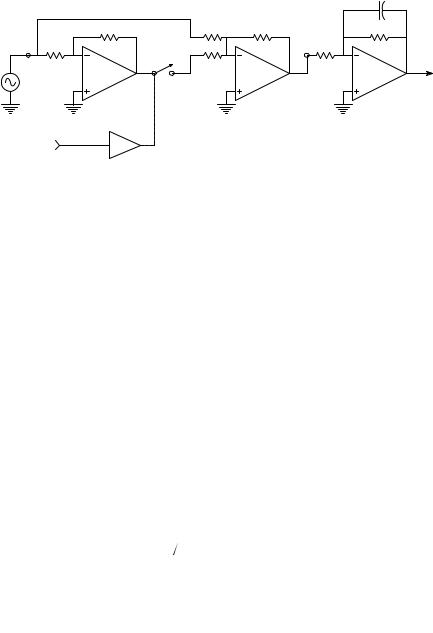
454 |
|
|
Analysis and Application of Analog Electronic Circuits |
||
|
|
|
|
|
C |
|
|
R |
R |
R |
R |
|
|
R |
|
|
R |
|
|
|
|
|
___ |
|
|
OA1 |
R/2 |
|
vz(t) |
|
DSBSC |
−ym(t) MOS switch |
OA2 |
OA3 |
|
Vo’ |
|
|
vz(t) |
||
signal |
|
|
|||
LPF
vr(t)
SYNC
FIGURE 11.13
Schematic of a three-op amp synchronous (phase-sensitive) rectifier used to demodulate a DSBSC-modulated carrier.
version of a PSR, an analog MOS switch is made to close for the positive half-cycles of the reference signal that has the same frequency and phase as the unmodulated carrier. Figure 11.14 illustrates a low-frequency modulating signal, vm(t), from there, the DSBSCM signal, and, finally, Vz(t), the unfiltered output of the PSR. Note that “c” means the MOS switch is closed and “o” means it is open. The simple op amp low-pass filter also inverts, so its output Vz is proportional to −vm(t).
Another means of demodulating a DSBSC signal is by an analog multiplier followed by an LPF. In the latter means, the multiplier output voltage, Vo′(t), is the product of a reference carrier and the DSBSCM signal:
Vo′(t) = (0.1)Bcos(ωct) ∞ (A mo 2)[cos((ωc + ωm )t)+ cos((ωc − ωm )t)] (11.58)
The 0.1 constant is inherent to all analog multipliers. By trigonometric identity, noting that cosθ is an even function, the multiplier output can be written:
V′(t) = (0.1)(A m B 4) cos((2ω |
c |
+ ω |
m |
)t)+ cos(ω |
m |
t) |
(11.59) |
||
o |
o |
[ |
|
|
] |
|
|||
After unity-gain low-pass filtering,
|
(t) = (0.1)(AB 4)mo cos(ωmt) |
(11.60) |
Vo′ |
which is certainly proportional to vm(t).
Still another way to demodulate DSBSC signals is by a special PLL architecture called the Costas loop (Northrop, 1990), shown in Figure 11.15. Its successful operation requires that the modulating signal, vm(t), be nonzero
© 2004 by CRC Press LLC

Modulation and Demodulation of Biomedical Signals |
455 |
vm(t) |
t |
0 |
DSBSCM signal
0
|
Vz |
PSD signal |
|
|
|
|
|
|
|
|
|
(before LPF) |
|
|
|
|
|
|
|
|
|
|
|
|
|
|
|
|
|
|
|
|
|
|
|
|
|
|
|
|
Switch status |
|
|
0 |
c |
o |
c |
o |
c |
o |
c |
o |
c |
o |
|
|
|
|
|
|
|
|
|
|
FIGURE 11.14
Waveforms relevant to the operation of the synchronous rectifier of Figure 11.13. Top: Modulating signal. Middle: DSBSC signal. Bottom: Detected signal before LPF.
only for short intervals so that the PLL does not lose lock. The input DSBSCM signal can be written:
x1 = vm(t) Vc cos(ωct + θc) |
(11.61) |
The output of the PLL’s VCO is:
x6 = X6 cos(ωot + θo) |
(11.62) |
© 2004 by CRC Press LLC
456 |
Analysis and Application of Analog Electronic Circuits |
|
|
M1 |
|
x1 |
x2 |
x3 |
|
LPF1 |
|
x6 Kv |
x5 |
LPF3 |
x4 |
M3 |
s |
|
|
||
|
|
|
|
90o PS
x7
x8 |
x9 |
|
LPF2 |
M2
FIGURE 11.15
Block diagram of a simple Costas PLL.
and the output of mixer M1 is: |
|
x2 = x1 ∞ x6 = vm (t)VcX6 cos(ωct + θc )cos(ωot + θo ) |
(11.63) |
= [vm (t)Vc X6  2]{cos[(ωc + ωo )t + θc + θo ]+ cos[(ωc − ωo )t + θc − θo ]}
At lock, ωo ωc and θo θc, and LPF1 passes only the low-frequency components of x2. Thus:
x3 = vm(t) Vc X6/2 |
(11.64) |
which is the desired output.
Now examine how the other signals in the Costas loop contribute to its operation. By trigonometric identity, the output of the quadrature phase shifter is:
x7 = −X6 sin(ωot + θo) |
(11.65) |
The output of the second mixer is thus: |
|
x8 = −X6vm (t)Vc sin(ωot + θo )cos(ωct + θc ) |
(11.66A) |
x8 = [−X6vm (t)Vc  2]{sin[(ω0 + ωc )t + θo + θc ]+ sin[(ωo − ωc )t + θo − θc ]} (11.66B)
© 2004 by CRC Press LLC