

- •Analysis and Application of Analog Electronic Circuits to Biomedical Instrumentation
- •Dedication
- •Preface
- •Reader Background
- •Rationale
- •Description of the Chapters
- •Features
- •The Author
- •Table of Contents
- •1.1 Introduction
- •1.2 Sources of Endogenous Bioelectric Signals
- •1.3 Nerve Action Potentials
- •1.4 Muscle Action Potentials
- •1.4.1 Introduction
- •1.4.2 The Origin of EMGs
- •1.5 The Electrocardiogram
- •1.5.1 Introduction
- •1.6 Other Biopotentials
- •1.6.1 Introduction
- •1.6.2 EEGs
- •1.6.3 Other Body Surface Potentials
- •1.7 Discussion
- •1.8 Electrical Properties of Bioelectrodes
- •1.9 Exogenous Bioelectric Signals
- •1.10 Chapter Summary
- •2.1 Introduction
- •2.2.1 Introduction
- •2.2.4 Schottky Diodes
- •2.3.1 Introduction
- •2.4.1 Introduction
- •2.5.1 Introduction
- •2.5.5 Broadbanding Strategies
- •2.6 Photons, Photodiodes, Photoconductors, LEDs, and Laser Diodes
- •2.6.1 Introduction
- •2.6.2 PIN Photodiodes
- •2.6.3 Avalanche Photodiodes
- •2.6.4 Signal Conditioning Circuits for Photodiodes
- •2.6.5 Photoconductors
- •2.6.6 LEDs
- •2.6.7 Laser Diodes
- •2.7 Chapter Summary
- •Home Problems
- •3.1 Introduction
- •3.2 DA Circuit Architecture
- •3.4 CM and DM Gain of Simple DA Stages at High Frequencies
- •3.4.1 Introduction
- •3.5 Input Resistance of Simple Transistor DAs
- •3.7 How Op Amps Can Be Used To Make DAs for Medical Applications
- •3.7.1 Introduction
- •3.8 Chapter Summary
- •Home Problems
- •4.1 Introduction
- •4.3 Some Effects of Negative Voltage Feedback
- •4.3.1 Reduction of Output Resistance
- •4.3.2 Reduction of Total Harmonic Distortion
- •4.3.4 Decrease in Gain Sensitivity
- •4.4 Effects of Negative Current Feedback
- •4.5 Positive Voltage Feedback
- •4.5.1 Introduction
- •4.6 Chapter Summary
- •Home Problems
- •5.1 Introduction
- •5.2.1 Introduction
- •5.2.2 Bode Plots
- •5.5.1 Introduction
- •5.5.3 The Wien Bridge Oscillator
- •5.6 Chapter Summary
- •Home Problems
- •6.1 Ideal Op Amps
- •6.1.1 Introduction
- •6.1.2 Properties of Ideal OP Amps
- •6.1.3 Some Examples of OP Amp Circuits Analyzed Using IOAs
- •6.2 Practical Op Amps
- •6.2.1 Introduction
- •6.2.2 Functional Categories of Real Op Amps
- •6.3.1 The GBWP of an Inverting Summer
- •6.4.3 Limitations of CFOAs
- •6.5 Voltage Comparators
- •6.5.1 Introduction
- •6.5.2. Applications of Voltage Comparators
- •6.5.3 Discussion
- •6.6 Some Applications of Op Amps in Biomedicine
- •6.6.1 Introduction
- •6.6.2 Analog Integrators and Differentiators
- •6.7 Chapter Summary
- •Home Problems
- •7.1 Introduction
- •7.2 Types of Analog Active Filters
- •7.2.1 Introduction
- •7.2.3 Biquad Active Filters
- •7.2.4 Generalized Impedance Converter AFs
- •7.3 Electronically Tunable AFs
- •7.3.1 Introduction
- •7.3.3 Use of Digitally Controlled Potentiometers To Tune a Sallen and Key LPF
- •7.5 Chapter Summary
- •7.5.1 Active Filters
- •7.5.2 Choice of AF Components
- •Home Problems
- •8.1 Introduction
- •8.2 Instrumentation Amps
- •8.3 Medical Isolation Amps
- •8.3.1 Introduction
- •8.3.3 A Prototype Magnetic IsoA
- •8.4.1 Introduction
- •8.6 Chapter Summary
- •9.1 Introduction
- •9.2 Descriptors of Random Noise in Biomedical Measurement Systems
- •9.2.1 Introduction
- •9.2.2 The Probability Density Function
- •9.2.3 The Power Density Spectrum
- •9.2.4 Sources of Random Noise in Signal Conditioning Systems
- •9.2.4.1 Noise from Resistors
- •9.2.4.3 Noise in JFETs
- •9.2.4.4 Noise in BJTs
- •9.3 Propagation of Noise through LTI Filters
- •9.4.2 Spot Noise Factor and Figure
- •9.5.1 Introduction
- •9.6.1 Introduction
- •9.7 Effect of Feedback on Noise
- •9.7.1 Introduction
- •9.8.1 Introduction
- •9.8.2 Calculation of the Minimum Resolvable AC Input Voltage to a Noisy Op Amp
- •9.8.5.1 Introduction
- •9.8.5.2 Bridge Sensitivity Calculations
- •9.8.7.1 Introduction
- •9.8.7.2 Analysis of SNR Improvement by Averaging
- •9.8.7.3 Discussion
- •9.10.1 Introduction
- •9.11 Chapter Summary
- •Home Problems
- •10.1 Introduction
- •10.2 Aliasing and the Sampling Theorem
- •10.2.1 Introduction
- •10.2.2 The Sampling Theorem
- •10.3 Digital-to-Analog Converters (DACs)
- •10.3.1 Introduction
- •10.3.2 DAC Designs
- •10.3.3 Static and Dynamic Characteristics of DACs
- •10.4 Hold Circuits
- •10.5 Analog-to-Digital Converters (ADCs)
- •10.5.1 Introduction
- •10.5.2 The Tracking (Servo) ADC
- •10.5.3 The Successive Approximation ADC
- •10.5.4 Integrating Converters
- •10.5.5 Flash Converters
- •10.6 Quantization Noise
- •10.7 Chapter Summary
- •Home Problems
- •11.1 Introduction
- •11.2 Modulation of a Sinusoidal Carrier Viewed in the Frequency Domain
- •11.3 Implementation of AM
- •11.3.1 Introduction
- •11.3.2 Some Amplitude Modulation Circuits
- •11.4 Generation of Phase and Frequency Modulation
- •11.4.1 Introduction
- •11.4.3 Integral Pulse Frequency Modulation as a Means of Frequency Modulation
- •11.5 Demodulation of Modulated Sinusoidal Carriers
- •11.5.1 Introduction
- •11.5.2 Detection of AM
- •11.5.3 Detection of FM Signals
- •11.5.4 Demodulation of DSBSCM Signals
- •11.6 Modulation and Demodulation of Digital Carriers
- •11.6.1 Introduction
- •11.6.2 Delta Modulation
- •11.7 Chapter Summary
- •Home Problems
- •12.1 Introduction
- •12.2.1 Introduction
- •12.2.2 The Analog Multiplier/LPF PSR
- •12.2.3 The Switched Op Amp PSR
- •12.2.4 The Chopper PSR
- •12.2.5 The Balanced Diode Bridge PSR
- •12.3 Phase Detectors
- •12.3.1 Introduction
- •12.3.2 The Analog Multiplier Phase Detector
- •12.3.3 Digital Phase Detectors
- •12.4 Voltage and Current-Controlled Oscillators
- •12.4.1 Introduction
- •12.4.2 An Analog VCO
- •12.4.3 Switched Integrating Capacitor VCOs
- •12.4.6 Summary
- •12.5 Phase-Locked Loops
- •12.5.1 Introduction
- •12.5.2 PLL Components
- •12.5.3 PLL Applications in Biomedicine
- •12.5.4 Discussion
- •12.6 True RMS Converters
- •12.6.1 Introduction
- •12.6.2 True RMS Circuits
- •12.7 IC Thermometers
- •12.7.1 Introduction
- •12.7.2 IC Temperature Transducers
- •12.8 Instrumentation Systems
- •12.8.1 Introduction
- •12.8.5 Respiratory Acoustic Impedance Measurement System
- •12.9 Chapter Summary
- •References
Operational Amplifiers |
263 |
6.6Some Applications of Op Amps in Biomedicine
6.6.1Introduction
Op amps are extremely useful in the design of all sorts of analog electronic instrumentation systems. As demonstrated in Chapter 7 and Chapter 8, op amps find great application in the design of analog active filters and as building blocks for instrumentation amplifier (differential) amplifiers and other linear and nonlinear signal conditioning systems. As the preceding sections have shown, there are a number of specialized types of op amps for specific signal processing applications. The following sections focus on four applications that often have important roles in biomedical signal processing: integrators; differentiators; charge amplifiers; and an isolated two-op amp instrumentation DA useful for measuring ECG. This amplifier also includes a band-pass filter and an analog photo-optic coupler for galvanic isolation.
6.6.2Analog Integrators and Differentiators
A simple op amp integrator is shown in Figure 6.16. An op amp integrator is hardly ever used as a stand-alone component; it is usually incorporated as part of a feedback loop to obtain some desired dynamic characteristic for the closed-loop system. The reason for not using it alone is that it integrates its own dc bias current and offset voltage, causing its output, in the absence of an input signal, to drift into saturation slowly and linearly. In the circuit of Figure 6.16, set Vs = 0 and consider the op amp ideal, so vi′ = 0. Thus, the node voltage V1 must equal VOS. Using superposition, and considering IB and VOS to be steps applied at t = 0, the integrator’s time-domain output can be written:
Vo(t) = −t IB/CF + VOS (1 + t/RCF) |
(6.60) |
|
|
|
CF |
R |
V1 |
VOS |
|
+ |
|
||
|
|
vi’ |
Vo |
|
|
|
|
Vs |
IB |
|
IOA |
FIGURE 6.16
A dc model of a voltage op amp integrator. The op amp is assumed ideal and its offset voltage and bias current are externalized to its inverting (vi′ ) node. The integrator’s behavior is analyzed in the text.
© 2004 by CRC Press LLC
264 |
Analysis and Application of Analog Electronic Circuits |
||
|
|
|
CF |
|
|
|
R |
C |
vi’ |
ena |
|
|
|
||
|
|
ina |
Vo |
Vs |
|
OA |
|
|
|
|
|
FIGURE 6.17
Circuit for an op amp differentiator. In this problem, the op amp’s frequency response is considered, as well as its short-circuit input voltage noise root power spectrum, and input current noise root spectrum.
IB and VOS can have either sign, depending on the op amp design and its temperature. VOS magnitude is typically in the range of hundreds of microvolts and IB can range from tens of faradamperes to microamperes, again depending on OA design and temperature.
If stand-alone analog integration must be done, the integrator drift must be considered. Op amps with low VOS and IB are used and a means of shorting out CF is used to ensure zero initial conditions at the start of integration. Digital integration is no panacea; it will integrate small analog offset voltages present in the anti-aliasing filter, the sample and hold, and the ADC.
Often, when an integrator is used in a closed-loop system, it is desirable to give its transfer function a real zero, as well as the pole at the origin. The zero is used to give the system better closed-loop dynamic performance and is easily obtained by placing a resistance, RF, in series with CF. Assuming an ideal op amp, the transfer function is:
Vo |
|
RF + 1 sCF |
|
( |
s R C |
F |
+ 1 |
|
Ki (sτf |
+ 1) |
|
(s) = − |
= − |
F |
) |
= − |
|
|
(6.61) |
||||
V |
|
|
s RC |
|
s |
|
|||||
|
R |
F |
|
|
|||||||
s |
|
|
|
|
|
|
|
|
|
||
which is what is desired.
Figure 6.17 illustrates a conventional op amp analog differentiator. If the op amp is treated as ideal and CF is neglected, then the transfer function is:
Vo |
(s) = −s RC |
(6.62) |
|
V |
|||
|
|
||
s |
|
|
which is the transfer function of an ideal time-domain differentiator with gain −RC.
© 2004 by CRC Press LLC

Operational Amplifiers |
265 |
Now consider what happens to the differentiator’s transfer function when a real frequency-compensated op amp is modeled by the open-loop gain:
|
Vo |
−Kvo |
|
||||
|
|
(s) = |
|
|
|
|
(6.63) |
|
V′ |
τ |
A |
s + 1 |
|||
|
i |
|
|
|
|
||
Now the node equation on the Vi′ node is: |
|
||||||
Vi′ (G + s C) − Vo G = Vs s C |
(6.64) |
||||||
Using Equation 6.63, Vi′ in Equation 6.64 can be eliminated and the overall transfer function written:
Vo |
(s) = |
−s RC Kvo (1+ Kvo ) |
|
|
s2 τA RC (1+ Kvo )+ s(τA + RC) |
(1+ Kvo )+ 1 |
|
Vs |
|||
|
|
|
(6.65) |
−s RC
s2 τARC Kvo + s(τA + RC) Kvo + 1
Note that Equation 6.65 has the form of the transfer function of a quadratic band-pass filter shown in the following equation:
V |
(s) = |
|
|
−s K |
|
|
(6.66) |
o |
|
|
|
|
|
||
V |
s2 |
ω 2 |
+ s 2ξ ω |
n |
+ 1 |
||
s |
|
|
n |
|
|
|
From Equation 6.66 and Equation 6.65, the resonant frequency is:
ωn Kvo (τARC) r s |
(6.67) |
||||
and the damping factor is: |
|
|
|
|
|
ξ = |
(τA + RC) |
|
Kvo |
|
(6.68) |
2 Kvo |
|
τARC |
|||
|
|
|
|||
When typical numerical values are substituted for the op amp and circuit
parameters (Kvo = 106; τA = 0.001 sec; R = 106 Ω; and C = 10−6 F), ωn = 3.16 ∞ 104 r/s and ξ = 1.597 ∞ 10−2. This damping is equivalent to a quadratic BPF
Q = 1/(2ξ) = 31.3, which is a sharply tuned filter. Thus, any fast transients in Vs will excite a poorly damped sinusoidal transient at the differentiator output.
© 2004 by CRC Press LLC

266 |
Analysis and Application of Analog Electronic Circuits |
Another problem with the simple R–C differentiator is the differentiation of the op amp’s short-circuit equivalent voltage noise, ena. The transfer function for ena is easily shown to be:
Vo = Ena (1 + s RC) |
(6.69) |
Because ena has a broadband spectrum, the differentiator’s output noise has a spectrum that increases with frequency, making the output very noisy. (Note that the ina component in Vo is not differentiated.) When a feedback capacitor, CF, is added in parallel with R, the differentiator’s frequency response is found from the new node equation:
Vi′[G + s(C + CF )]− Vo (G + sCF ) = Vs sC |
(6.70) |
Using Equation 6.63, Vi′ in the preceding equation can be eliminated and the transfer function written:
Vo |
(s) = |
−s RC |
|
|
s2 τAR(C + CF ) Kvo + s[(τA + RC) Kvo + RCF ]+ 1 |
(6.71) |
|
Vs |
The differentiator transfer function still has the format of a BPF. Examine its ωn and damping: all parameters are the same as the preceding ones and CF = 6.7 ∞ 10−11 F (67 pF).
ω 2 = |
Kvo |
= |
106 |
|
= 9.99933 ∞ 108 |
|
τAR(C + CF ) |
10−3 ∞ 106 ∞ (10−6 |
+ 6.7 ∞ 10−11) |
||||
n |
|
|
||||
|
|
|
|
|
¬
ωn = 3.1622 ∞ 104 r/s
The damping factor is now found from:
2ξ ω |
n |
= |
τA + RC |
+ RC |
|
|
||||||
|
|
|
|
|||||||||
|
|
|
|
|
Kvo |
F |
|
|
||||
|
|
|
|
|
|
|
|
|
|
|||
ξ = 0.5 ∞ 3.1622 ∞ 104 |
|
10−3 + 1 |
+ 6.7 ∞ 10−11 ∞ 106 |
ˆ |
= 1.075 |
|||||||
|
|
|
|
|
|
|
˜ |
|||||
|
10 |
6 |
|
|
||||||||
|
|
|
|
|
|
|
|
↓ |
|
|||
(6.72)
(6.73)
(6.74)
(6.75)
The ωn has changed little, but now the system is slightly overdamped, i.e., both poles are close on the real axis in the s-plane. The differentiator’s frequency response is still band pass with its peak gain at the same frequency,
© 2004 by CRC Press LLC

Operational Amplifiers |
|
|
267 |
|
|
|
GF |
|
|
|
CF |
|
|
|
vi’ |
• |
|
|
Vo |
ix = F d |
CT |
GT |
EOA |
FIGURE 6.18
An electrometer op amp is used to make a charge amplifier to condition the output of a piezoelectric force transducer. See text for analysis.
but is no longer severely underdamped. Making CF larger will make the system more overdamped; it will have two real poles, one below ωn and the other above it. Thus, for practical reasons, an op amp, analog differentiator should have a small feedback capacitor in parallel with the feedback R to limit its bandwidth and give it reasonable damping so that input noise spikes will not excite “ringing” in its output.
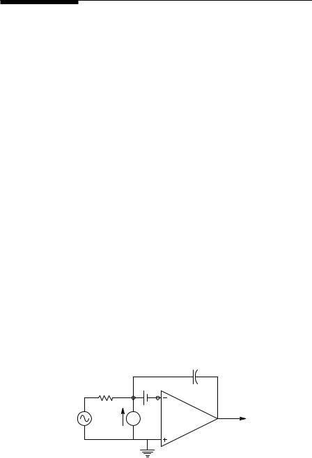
6.6.3Charge Amplifiers
A charge amplifier is used to condition the output of a piezoelectric transducer used in such applications as accelerometers, dynamic pressure sensors, microphones, and ultrasonic receivers. Figure 6.18 illustrates the schematic of an electrometer op amp used as a charge amplifier. The shunt capacitance, CT, includes the capacitance of the piezotransducer, the connecting coax (if any), and the input capacitance of the op amp. Similarly, the conductance GT includes the leakage conductance of the transducer, the connecting cable, and the op amp’s input conductance. The op amp is assumed to have a finite gain and frequency response, i.e., it is nonideal in this respect. Thus, the summing junction voltage, vi′, is finite. The op amp’s gain is modeled by:
V = −V′ |
Kvo |
|
(6.76) |
||
τ s + 1 |
|||||
o |
i |
|
|||
The node equation for the summing junction is: |
|
||||
Vi′[s(CF + CT )+ GT + GF ]− Vo[sCF + GF ] = F(s)d = sF(s)d |
(6.77) |
||||
from which:
© 2004 by CRC Press LLC
268 |
|
|
|
Analysis and Application of Analog Electronic Circuits |
||||||
|
|
|
|
Vi′= |
sF(s)d + Vo[sCF + GF |
] |
|
|
||
|
|
|
|
[s(CF + CT )+ CT + GF |
] |
|
(6.78) |
|||
|
|
|
|
|
|
|
¬ |
|
|
|
|
|
|
V |
τs + |
1 = −K |
s F(s)d + Vo[sCF |
+ GF ] |
(6.79) |
||
|
|
|
vo [s(CF + CT )+ GT |
+ GF ] |
||||||
|
|
|
o[ |
|
] |
|
|
|||
|
|
|
|
|
|
|
¬ |
|
|
|
|
Vo |
(s) = |
|
|
|
|
−s Kvo d |
|
|
|
|
|
s2τ(CF + CT )+ s[τ(GF + GT )+ CF + CT + KvoCF ]+ KvoGF |
(6.80) |
|||||||
|
F |
|||||||||
To put Equation 6.80 into time-constant format, divide top and bottom by Kvo GF and note that certain terms in the denominator are negligibly small. Let s = jω in order to write the charge amplifier’s frequency response:
Vo |
(jω) |
− jω d RF |
(6.81) |
F |
(jω)2 τ(CF + CT )RF Kvo + jω CFRF + 1 |
The frequency response function of Equation 6.81 is band pass with two real poles. The low-frequency one is set by the feedback R and C and is s1
−1/(RFCF) r/s; the high-frequency pole can be shown to be approximately s2 −(Kvo/τ)[CF/(CF + CT)] = ωT CF/(CF + CT) r/s. ωT is the op amp’s radian gain-bandwidth product. For example, set Kvo = 106; τ = 10−3 sec; CF = 10−9 F;
CT = 10−9 F; GF = 10−10 S; and GT = 10−12 S. Now the low break frequency is at flo = 1.59 ∞ 10−2 Hz and the high break frequency is at fhi = 80 MHz, which is adequate for conditioning 5-MHz ultrasound.
6.6.4A Two-Op Amp ECG Amplifier
Op amps can be used to make high-gain differential amplifiers with high common-mode rejection ratios, as described in Section 3.7.2 in Chapter 3. The two-op amp DA was found to have a DM gain:
Vo = (Vs − Vs′) 2(1 + R/RF) |
(6.82) |
R and RF should be chosen so that the amplifier’s DM gain is 103. To use this amplifier as an ECG system front end, it is necessary to define the ECG band pass with a highand low-pass filter. An easy design is to cascade the Sallen and Key high-pass and low-pass filters, as shown in Figure 6.19. The HPF is given complex-conjugate poles with an fn = 0.1 Hz and a damping
factor of ξ = 0.707. Using the design formulas given in Section 7.2.2 in Chapter 7, C1 = C2 = C and, for ξ = 0.707, R1 = 2 R2. fn = 1/(2πC R1R2) = 0.1,
© 2004 by CRC Press LLC

Operational Amplifiers |
|
|
269 |
|
|
C1 |
|
R1 |
HPF |
LPF |
|
C |
|
V2 R |
|
V1 |
|
O R C2 |
V3 |
C |
OA |
A |
|
|
R2 |
|
|
FIGURE 6.19
A band-pass filter for electrocardiography made from cascaded Sallen and Key high-pass filter and low-pass filters.
so one can solve for R1 and R2 after choosing C = 3.3 μF. A little algebra gives R2 = 3.31 ∞ 105 and R1 = 6.821 ∞ 105 Ω.
The parameters for the S and K LPF are found from ξ = C2/C1 = 0.707 and fn = 1/(2πR C1C2) = 100 Hz. Clearly, C2 = 2C1 for the desired damping. Choose C1 = 0.1 μF, so C2 = 0.2 μF. Using the fn relation, R = 1.125 ∞104 Ω. The op amps need not be special low-noise or high fT designs, the ECG signal has limited bandwidth, and the noise performance is set by the differential front end amplifier having the gain of 103.
Now that the ECG signal has been amplified and its bandwidth defined, it is necessary to consider patient galvanic isolation. One easy way to achieve isolation is to run the DA and filter op amps on isolated battery power with no ground connection common with the power line mains. A pair of 12-V batteries can be used with IC voltage regulators to give ±8 V to run the four signal conditioning op amps. One cannot simply connect the output of the filter to an oscilloscope or computer to view the ECG. The common ground from the oscilloscope or computer destroys patient galvanic isolation, so some means of coupling the signal without the necessity of a common ground must be used. One means is to sample the isolated ECG and convert it with a serial output isolated ADC and then couple the digitized ECG to the outside using a photo-optic coupler (POC). (A transformer can also be used.) The digitized ECG must then be converted to analog form with a serial input DAC in order to be viewed on an oscilloscope or be an input to a strip-chart recorder.
A simpler form of galvanic isolation that uses POCs and gives an analog output is shown in Figure 6.20. OA1 is run from the isolated battery power supply of the signal conditioner. The top LED in the dual POC IC is biased on with the 3-mA dc current source, causing an average light intensity, I1o, to be emitted. The isolated conditioned ECG output, V3, causes the light intensity to vary proportionally around the average level, I1o. The light from LED1 is transmitted through a plastic light guide to photodiode, PD2. An increase in the light hitting the photojunction of PD1 causes a proportional increase in its (reverse) photocurrent. PD1’s increased photocurrent is the base current of the top npn BJT, so its collector current increases, causing the inverting input of op amp OA2 to go negative and making OA2’s output go positive. The positive increment on OA2’s output increases the current in
© 2004 by CRC Press LLC