

Wasserscheid P., Welton T. - Ionic Liquids in Synthesis (2002)(en)
.pdf306 Frank Endres
The left side is essentially identical to the potentiostat circuit presented in Section 6.2.1.2.. The right side is the preamplifier of the STM. The atomically sharp metal tip is located roughly 1 nm over an electronically conductive substrate, here the working electrode (WE) of interest. This is done by computer control, with the help of step motors and micrometer screws as well as piezoelectric elements, to which the tip is connected. If a potential U2 is applied between tip and sample (typically 5–500 mV) a tunneling current I(t) flows, with typical values between 0.1 and 10 nA, depending on the distance. This current is transformed into a voltage U3 (= –R*I(t)) that can be further processed. The tunneling current is strongly dependent on the distance (d) and is a function of the electronic density of states of tip D (tip) and sample D (sample). For a strongly simplified case one obtains to a first approximation Equation 6.2-2 [64]:
I(tunnel) = f(U bias) * D(tip) * D(sample) * exp[- const. * d] |
(6.2-2) |

6.2 Making of Inorganic Materials by Electrochemical Methods 307
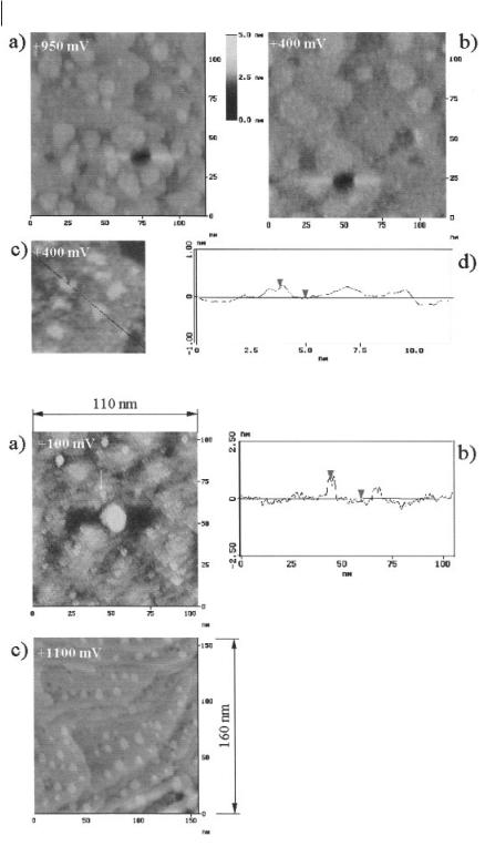
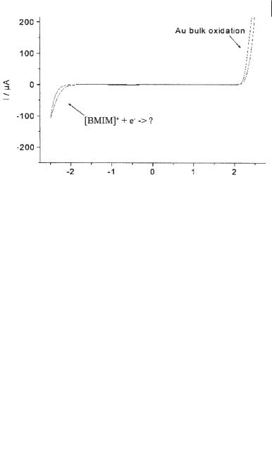
Cyclic voltammogram of acid [BMIM]+Cl–/AlCl3 on Au(111): Au oxidation begins at electrode potentials > +1.2 V vs. Al/AlCl3. UPD processes are observed at about +900 and +400 mV before bulk deposition of Al starts (see also [65]).
The following electrode processes at the surfaces have been identified during electrodeposition. Upon a potential step from E > +1000 mV to E = +950 mV vs. Al/AlCl3, two-dimensional islands formed irreversibly on the surface. Their height was 250 ± 20 pm, indicative of gold islands. We attributed this observation to the formation of Au–Al compounds followed by expulsion of surplus Au atoms to the surface. At an electrode potential of +400 mV, small Al islands with an averaged height of 230 ± 20 pm started growing (Figure 6.2-4).
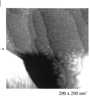
At +100 mV vs. Al/AlCl3, clusters of up to 1 nm in height formed. When a potential step to +1100 mV vs. Al/AlCl3 was performed, the clusters dissolved immediately, but both holes and gold islands of up to two monolayers in height remained on the surface. It is likely that strong alloying between Au and Al took place both in the surface and in the deposited clusters (Figure 6.2-5).
In the overpotential deposition regime we observed that nanosized Al was deposited in the initial stages. Furthermore, a transfer of Al from the scanning tip to the Al covered substrate was observed. We accidentally succeeded in an indirect tip-induced nanostructuring of Al on growing Al (Figure 6.2-6).
These results are quite interesting. The initial stages of Al deposition result in nanosized deposits. Indeed, from the STM studies we recently succeeded in making bulk deposits of nanosized Al with special bath compositions and special electrochemical techniques [10]. Moreover, the preliminary results on tip-induced nanostructuring show that nanosized modifications of electrodes by less noble elements are possible in ionic liquids, thus opening access to new structures that cannot be made in aqueous media.
6.2 Making of Inorganic Materials by Electrochemical Methods 309
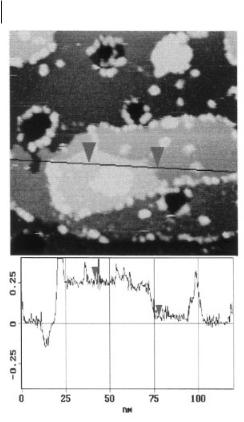
Underpotential phenomena during Al reduction in acidic [BMIM]+Cl–/AlCl3 on Au(111). At +950 mV vs. Al/AlCl3, two-dimensional islands with a height of 250 ± 20 pm form
(a). At +400 mV (b), two-dimensional Al islands with an averaged height of 230 ± 20 pm are reversibly deposited. In (c) the islands are shown with a higher resolution, while (d) shows a typical height profile.
Underpotential phenomena during Al reduction in acidic [BMIM]+Cl–/AlCl3 on Au(111): nanoclusters with heights of up to 1 nm form at +100 mV vs. Al/AlCl3 (a); a typical height profile is shown in (b). Upon a potential step to +1100 mV vs. Al/AlCl3 the clusters dissolve immediately and leave holes in the surfaces as well as small Au islands (c): alloying between Al and Au is very likely.
Copper electrodeposition on Au(111) Copper is an interesting metal and has been widely investigated in electrodeposition studies from aqueous solutions. There are numerous publications in the literature on this topic. Furthermore, technical processes to produce Cu interconnects on microchips have been established in aqueous solutions. In general, the quality of the deposits is strongly influenced by the bath composition. On the nanometer scale, one finds different superstructures in the underpotential deposition regime if different counter-ions are used in the solutions. A co-adsorption between the metal atoms and the anions has been reported. In the underpotential regime, before the bulk deposition begins, one Cu monolayer forms on Au(111) [66].
In situ STM experiments in an acidic [BMIM]Cl/AlCl3 ionic liquid with either CuCl or CuCl2 as copper sources have recently been carried out in the author’s group [67]. The motivation was based mainly on two facts: copper in chloroaluminates is deposited from Cu(I), and Cu+ can furthermore be regarded as a naked cation because there is no distinct solvation shell, unlike in aqueous media. As a consequence, distinct deviations from the behavior in aqueous solutions were expected. The cyclic voltammogram on Au(111) displayed three UPD processes, followed by three-dimensional Cu growth in the OPD regime. At potentials > +1000 mV vs. Cu/Cu+, gold oxidation starts first at the steps, at higher electrode potentials bulk oxidation of gold begins (Figure 6.2-7).
The following two pictures (Figure 6.2-8a and b) were acquired at +500 mV and at +450 mV vs. Cu/Cu+ and show that at +450 mV vs. Cu/Cu+ monolayer high Cu clusters nucleate at the steps between different Au terraces. Thus, the pair of shoulders in the cyclic voltammogram is correlated with this surface process.
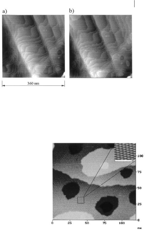
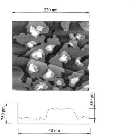
If the electrode potential is further reduced to +350 mV, a hexagonal superstructure with a periodicity of 2.4 ± 0.2 nm is observed. With respect to the interatomic distances in the Au(111) structure at the surface, this corresponds – within the error limits – to an 8 × 8 superstructure (Figure 6.2-9).
The integrated charge would correspond to 0.7 ± 0.1 Cu monolayers. Thus, either a less closely packed Cu layer or an anion co-adsorption that can both lead to a Moiré superstructure are probed; in the solution investigated [Al2Cl7]– is the predominant anion. At +200 mV vs. Cu/Cu+ the superstructure disappears and a completely closed Cu monolayer is observed, with a charge corresponding to 1.0 ± 0.1 Cu monolayers.
6.2 Making of Inorganic Materials by Electrochemical Methods 311
Underpotential phenomena during Cu reduction in acidic [BMIM]+Cl–/AlCl3 on Au(111): a potential step from +500 mV vs. Cu/Cu+ (a) to +450 mV results in the growth of small Cu islands at the steps of the gold terraces (b) (picture from [66] – with permission of the Pccp owner societes).
Unlike the case in aqueous solutions, the growth of a second 200 ± 20 pm high monolayer at +50 mV was observed, together with clusters of heights up to 1 nm (Figure 6.2-10).
This result is quite surprising, as no second Cu monolayer has yet been reported in aqueous solutions, nor have clusters up to 1 nm in height in the UPD regime. It
Figure 6.2-9: Underpotential phenomena during Cu reduction in acidic [BMIM]+Cl–/AlCl3 on Au(111): at +350 mV an 8 × 8 superstructure is observed; the integrated charge would correspond to 0.7 ± 0.1
Cu monolayers (picture from [66] – with permission of the Pccp owner societes).
312 Frank Endres
Figure 6.2-10: Underpotential phenomena during Cu reduction in acidic [BMIM]+Cl–/AlCl3 on Au(111): at +50 mV a second monolayer with a height of 200
± 20 pm grows, together with a pronounced deposition of clusters containing Cu and perhaps also a small amount of Al (picture from [66] – with permission of the Pccp owner societes).
cannot be excluded completely here that the clusters as well as the second monolayer could contain a small amount of Al. Such an underpotential alloying could stabilize the clusters enormously, especially as several stoichiometric Al-Cu compounds are known.
In the OPD regime, finally, the Cu bulk phase starts growing.
Germanium electrodeposition on Au(111) As a third example of in situ STM results, the electrodeposition of germanium should be mentioned here [59,60]. Germanium is an elemental semiconductor with a bandgap of 0.67 eV. In contrast to those of metals, furthermore, its crystal structure is determined by the tetrahedral symmetry of the Ge atoms, so that the diamond structure is thermodynamically the most stable. As the chemistry of Si and Ge are quite similar, such experiments could also give some insight into deposition process of the less noble Si. Germanium is hard to obtain in aqueous solutions, as its deposition potential is very close to that of hydrogen evolution. However, the ionic liquid [BMIM][PF6] (and others) can easily be prepared with water levels below 20 ppm and is therefore ideally suited for such electrodeposition studies. The pure liquid shows only capacitive behavior on Au(111), as can be seen in the cyclic voltammogram (Figure 6.2-11), acquired with a scan rate of 1 mV/s under inert gas conditions.
314
6.2 Making of Inorganic Materials by Electrochemical Methods 315
Figure 6.2-14: Bulk deposition of Ge on Au(111) in dry [BMIM]+ PF6–: at –2000 mV terraces with an average height of 330 ± 30 pm, indicative of Ge(111) bilayers, are obtained.
The surface consists of terraces of a height of 330 ± 30 pm. Within error limits, this is the value that would be expected for Ge(111) bilayers. Furthermore, we were able to observe that the electrodeposition gave rise to a less ordered surface structure with nanoclusters, transforming over a timescale of about 1 hour into a layered structure. With GeBr4 a transformation of clusters into such a layered surface was only partly seen; with GeCl4 this transformation could not be observed.
The oxidation of the deposited germanium is also a complicated process; we found that mainly chemical oxidation by GeI4 takes place, together with some electrooxidation. It is likely that kinetic factors play a dominant role.
If the germanium layers are partly oxidized by a short potential step to –1500 mV, random worm-like nanostructures form, healing in a complex process if the electrode potential is set back to more negative values (Figure 6.2-15).
As well as electrodissolution and electrodeposition, periphery and surface diffusion play important roles.
Unfortunately, only thin films of about 20 nanometers in thickness could be obtained with GeI4. An ex situ analysis was difficult, because of experimental limitations, but XPS clearly showed that elemental Ge was also obtained, besides