

2.5 Thin ®lm deposition procedures |
57 |
|
|
lasers. Laser ablation, sometimes called pulsed laser deposition (PLD), has typically been used to deposit ceramic materials, including high temperature superconductors (Dijkamp et al. 1987, Venkatasan et al. 1988, Morimoto & Shimizu 1995); it produces very rapid deposition in which whole chunks of material can break oV and be deposited during the immense peak powers which typically last for 10±20 ns. A particular advantage of rapid evaporation is the control of stoichiometry, since the diVerent species do not have time to segregate to the surface during the evaporation phase.
2.5.3Molecular beam epitaxy and related methods
The large scale use of such evaporation sources, especially for depositing semiconductor or metallic multilayers, has become known as molecular beam epitaxy (MBE). This acroymn has spawned several sub-cases, such as GSMBE (Gas Source MBE), and MOMBE (Metal±Organic MBE) which is sometimes called CBE (chemical beam epitaxy). Thus MBE really spans a range of techniques which range from being merely a fancy name for thermal evaporation, to much more chemically oriented ¯ow process techniques such as chemical vapor deposition (CVD) and MOCVD which we describe brie¯y in section 2.5.5. MBE is covered in several books (e.g. Parker 1985, Tsao 1993, Glocker & Shah 1995) and in many review articles and ongoing conference series. Only a few general points can usefully be made here, but this preparation method lies behind much of the science discussed later in chapters 5±8.
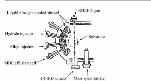
The growth end of such a chamber used for GSMBE or MOMBE is shown schematically in ®gure 2.8 (Abernathy 1995). The halfspace in front of the substrate is a bank of eVusion cells and various forms of gas injector cells, which transport reacting chemicals to the substrate. The growth of III±V compounds such as GaAs or AlGaAs has been pursued using such techniques, starting from metal±alkyl compounds such as
triethylaluminum (TEA) and triethylgallium (TEG) and hydrides such as AsH3. The group ®ve hydrides are injected via cracker cells which convert them catalytically into
As2 and hydrogen, which then impinge on the substrate to react with the alkyl beam to produce the growing ®lm (Panish & Sumski 1984, Abernathy 1995).
These cells are surrounded by liquid nitrogen cooled shrouds, which both condense unwanted evaporants and improve the vacuum in the sample region, which is monitored by the mass spectrometer. One of the advantages of MBE and related methods is the relative ease by which in situ diagnostic tools can be incorporated into the vacuum system. The most widely used are RHEED, shown in ®gure 2.8 and described in section 3.2.2, plus various optical techniques, some of which can also work in higher pressure environments. A compendium of these `real-time diagnostics', particularly in the context of semiconductor growth, is given by several authors in Glocker & Shah (1995, part D).
2.5.4Sputtering and ion beam assisted deposition
There are many uses for ions in connection with the production of thin ®lms. Sputtering using relatively low energy (100 eV±2 keV) ions is often used for cleaning samples, while higher energy (5±200 keV) ions can be used for doping layers with
58 2 Surfaces in vacuum
Figure 2.8. GSMBE or MOMBE growth chamber containing eVusion and cracker cells, and RHEED diagnostics (after Abernathy 1995, reproduced with permission). See text for discussion.
electrically active impurities. Ions can also be used for deposition, where individual ions, or charged clusters can be deposited at a range of energies. Clearly, the fact that the ions are charged allows extra control, and there are various methods by which this can be done. Directed ion beams from an accelerator form the most obvious possibility, but plasma and magnetron sources are also widely used (Bunshah 1991, Vossen & Kern 1991, Shah 1995, Smith 1995).
One of the main claims for IBAD (Ion Beam Assisted Deposition) or IBSD (Ion Beam Sputter Deposition) is that better quality deposits can be obtained at lower substrate temperatures, thus avoiding large scale interdiVusion which results from high temperature processing. However, the deposited ®lms adhere well to the substrate because of the localized limited mixing caused by the ion impacts (Itoh 1989, 1995, Marton 1994). This is one example of device engineers trying to reduce the `thermal budget' and so produce sharper interfaces between dissimilar components. Another possibilty is to produce clusters in a supersonic expansion source, and to ionize them, controlling their ¯ight during cluster depostion with applied voltages. This has been termed ICB (Ionized Cluster Beam) technology by the inventers (Takagi 1986, Takagi & Yamada 1989). Yet another possibility is to use ion beams to react with the substrate and grow compounds such as oxides or nitrides at and near surfaces (Herbots et al. 1994).
All of these procedures are inherently complex; for almost all purposes the question is whether they produce `better' ®lms for particular applications, i.e. whether they give a large enough improvement over existing methods to justify the considerable investment involved. Although our aim here is to give an outline description, we will not pursue models of how of these methods work in any detail; they are all rather speci®c to the combination of material and ion beam technique, and whether the processes are reactive, in the sense of involving (ion) chemistry, or physical, meaning that only collisions and clustering are involved. Nonetheless, ion beam assisted methods are very

2.5 Thin ®lm deposition procedures |
59 |
|
|
|
reactor wall |
|
|
input |
|
output |
|
H2 |
gas phase reactions |
|
|
SiH4 |
diffusion |
surface |
diffusion |
|
|
|
|
|
adsorption |
processes |
desorption |
(a)
Growth rate
(b)
substrate
surface gas kinetics
transport
thermodynamics
gas velocity
Figure 2.9. (a) Schematic diagram of reactions involved in the CVD of silicon from silane (SiH4) and hydrogen (H2); (b) typical variation of the growth rate on gas velocity with rate limiting steps indicated (after Vescan 1995, reproduced with permission).
widespread and are of great economic importance; sputter deposition in particular has high throughput for the production of (textured) polycrystalline thin ®lms of a wide variety of materials (Bunshah 1991, Vossen & Kern 1991, Shah 1995). The language used to describe such ion based processes (see Greene 1991) necessarily starts from a similar vantage point to that used to describe thermal evaporation; the latter topic is treated here in detail in chapter 5.
2.5.5Chemical vapor deposition techniques
The growth of semiconductor layers for device production is most frequently done by a variant of CVD (Chemical Vapor Deposition). This is usually implemented as a ¯ow technique in which the reacting gases pass over a heated substrate, as indicated in ®gure 2.9(a) for growth of silicon from silane and hydrogen. CVD reactors are either of the hot wall or cold wall type, and are surrounded by an extended gas handling and pumping system with rigorous control of the (often highly toxic) gases (Carlsson 1991, Vescan 1995). Because the pressure may be up to an atmosphere in certain cases (APCVD: Atmospheric Pressure CVD) the growth rate can be high, and UHV technology is not an absolute necessity; but control of impurities is a dominant problem, as pointed out in section 2.4.4 (O'Hanlon 1994). Thus UHV-CVD is becoming more widespread, where
the total pressure is ,1 mbar. However, most commercial processing corresponds to