


7.2 Case studies of reconstructed semiconductor surfaces |
239 |
|
|
Table 7.2. Calculated energies of reconstructed Si and Ge(111) surfaces (eV/13 1 cell)
|
131 |
231 |
232 |
333 |
535 |
737 |
Material |
relaxed |
cleaved |
adatom |
DAS |
DAS |
DAS |
|
|
|
|
|
|
|
Si(111) |
1.39b |
1.239d |
1.12b |
1.196c |
1.168c |
1.153c, 1.179d |
Ge(111) |
1.15a |
|
1.04a |
0.88a |
|
|
|
,1.34 ,1.40b |
|
,1.08 ,1.20b |
|
|
|
|
|
|
|
|
|
|
References: (a) Payne (1987), Payne et al. (1989); (b) Meade & Vanderbilt (1989). The Ge calculations were not well converged, and should be lower than the Si values; the ,values assume that the changes on convergence are the same as for Si; (c) Stich et al. (1992); (d)
Brommer et al. (1992). The only experimental values available date from 1960 and are
1.24 J´m22 for cleaved Si(111) (0.998 eV/131 cell) and 1.10 J´m22 for Ge(111) (0.952 eV/131 cell) (Kern et al. 1979); these values are not unreasonable, but they have unknown error bars.
adatom movement, and can nucleate 2D islands or pits; the microstructure thus becomes very complex, depending on the kinetics in detail.
7.2.4Si, Ge and GaAs(001), steps and growth
The geometry of the basic 231 reconstruction of Si(001) was fully described in section
1.4.We need to recall the formation of the dimers, their organization into dimer rows (perpendicular to the dimers), and the correlation with surface steps (Chadi 1979, 1989, GriYth & Kochanski 1990). There has been much debate as to whether the 23 1 reconstruction is symmetric, or asymmetric; by now you will realize that this is the same question as whether the surface is metallic or semiconducting. A consensus has emerged that the Si dimer is asymmetric, but that the energies are so close that the dimer ¯ips between two equivalent states ± either the left-hand or the right-hand atom is up at any one time. At high temperature, this is like having a low frequency anharmonic vibrational mode; at low temperature, ordered arrays of up and down dimers can give various superstructures, such as p232 or c234.
There are a host of such calculations in the literature: one (Ramstad et al. 1995) gives the c432 as the lowest energy structure, and calculates by how much it is stable. The dimerization gives a large energy gain over the unreconstructed 131 structure, about 2 eV per dimer. The asymmetric dimer is favored by a further 0.2 eV; ordering these dimers into either the p232 or c432 gains a further 0.02 eV, and the eventual stability of the c432 is a mere 0.002 eV/dimer. It is not entirely clear whether we should believe this slender margin, but it is clear why the complex superstructures will not be stable at high temperatures. Finite temperature molecular dynamics simulations have mapped out the timescale on which the dimers ¯ip between the two positions; an example which takes account of the actual p232 or c432 structure is shown in ®gure
7.9(Shkrebtii et al. 1995). Here it can be seen that dimers ¯ip, and also twist, causing
240 7 Semiconductor surfaces and interfaces
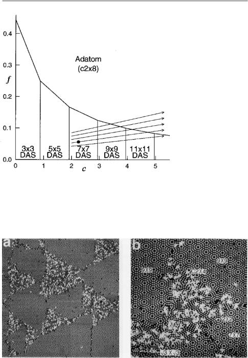
Figure 7.7. Model phase diagram of surface structures for the Si(111) surface; c and f are measures of the eVective corner hole and stacking fault energies relative to the dimer (domain wall) energies. The arrows show possible trajectories that can occur by increasing the adatom density, and hence the chemical potential of Si which acts to compress the surface phase (after Vanderbilt 1987, and Yang & Williams 1994, reproduced with permisison).
(a) |
|
(b) |
|
|
|
Figure 7.8. Coexistence of reconstructions on Si(111) (a) area approximately 1003 100 nm2 showing 737, 939 and regions with higher densities of adatoms; (b) atomically resolved image of a high adatom density area 43343 nm2 showing 737, 939 and other reconstructions where adatoms are seen individually (after Yang & Williams 1994).

7.2 Case studies of reconstructed semiconductor surfaces |
241 |
|
|
Figure 7.9. Dimer buckling (z-motion) and twisting (y-motion) on Si(001) revealed in a ®nite temperature molecular dynamics simulation at 900 K, showing two of the four dimers in a (432) cell (after Shkrebtii et al. 1995, reproduced with permission).

2427 Semiconductor surfaces and interfaces
changes of structure, roughly every 0.5±1 ps. The amplitudes are suprisingly large, namely .0.05 nm up and down (buckling) and sideways (twist plus shift) ,0.03 nm at
900 K. These amplitudes correspond to tilt angles in the range 16±19°, though this value does vary somewhat between the diVerent calculations (Krüger & Pollmann 1994, 1995, Ramstad et al. 1995, Srivastava 1997).
For Ge (001), and more recently Ge/Si (001) also, there has been great interest in whether these surfaces are also asymmetric, in what way, and in establishing the trends in bond angles (Tang & Freeman 1994). All these reconstructions reduce the symmetry of the surface, which results in diVusion and growth properties that are very anisotropic, and alternate across single height steps. The growth of devices based on Ge/Si(001), or GaAs on Si or Ge(001) gives rise to many fascinating problems. There is a vast literature on these topics, and even more unpublished empirical knowledge in the ®rms who make devices based on such materials. Some of these issues are aired in section 7.3; but the last word on these subjects is a long way in the future.
7.3Stresses and strains in semiconductor ®lm growth
7.3.1Thermodynamic and elasticity studies of surfaces
In the previous section we referred to the eVects of stress on surface reconstructions. Before proceeding further it is time to return to section 1.1.3, where it was noted that
surface stress had the same units as surface energy, but that the stress sij, sometimes written fij, is a second rank tensor, whereas the surface energy g is a scalar quantity. This complication is the main reason for delaying consideration of surface stress until
now. Somehow, the stress has potential to do work, but doesn't actually do so unless
there is a surface strain «ij associated with it. In that case the stored internal energy, assuming linear elasticity, is given as in bulk material by
DU51¤2osij«ij, |
(7.3) |
where the summation is assumed to be over repeated suYces, and in the case of a surface i, j51 or 2. The creation of a new surface, area A, in a strained solid proceeds in two stages in either order: we can strain the solid ®rst and then create the surface, or vice versa. The work done, dW analogous to (1.3) is then
dW5d(gA)5gdA1Adg. |
(7.4) |
Noting that dW5Aosijd«ij we can then deduce the relation for the individual components of the stress tensor
sij5gdij1-g/-«ij, |
(7.5) |
since dA5Adijd«ij, where dij is the Kronecker delta (i.e. 1 for i5j and zero otherwise). If the surface has three-fold rotation symmetry or higher, then the oV-diagonal terms of (7.5) are zero and the diagonal terms are equal, so the surface stress s is isotropic in the surface plane.
7.3 Stresses and strains in semiconductor ®lm growth |
243 |
|
|
The thermodynamic background leading to (7.5) is given by Cammarata (1994), who acknowledges that there has historically been much confusion on this topic. In addition, his paper describes calculations on the values of surface and interface stresses in particular materials. For example, noble metals are under positive surface stress if they have unreconstructed surfaces, because the surface atoms want to immerse themselves in a higher electron density to compensate for the loss of neighbors caused by the surface. The stress of the unreconstructed surfaces is calculated to be much larger for Au than for Ag; this is consistent, qualitatively at least, with the fact that Au(111) has the contracted 2331 herringbone structure, and Au(001) the more close-packed 5320 structures described in section 6.1.2, whereas Ag(111) and (001) are both unreconstructed (Needs et al. 1991). For semiconductors such as Si and Ge(111), the diVerent reconstructions are calculated to have diVerent surfaces stresses as well as energies, and indeed it is thought that the stability of the 737 reconstruction results from partial compensation of positive and negative stresses between diVerent layers (Meade & Vanderbilt 1989). However, the point to remember is that the stability of these surfaces depends on the surface energy, not the stress; the existence of the stress is only a reason why the surface might want to adopt a diVerent structure.
This situation changes if we apply a stress to the surface by external means; now work can be done by and on the surface, and the con®guration of the surface may change in response to the applied stress. The 231 reconstruction on Si(001), discussed in detail in section 1.4.4, is only mirror (2mm) symmetric, and so the surface stress tensor is not isotropic. Since single-height steps are associated with a switch in domain orientation, there is a change in surface stress across each step, and this can be portrayed as a force monopole F0 at each step, alternating in sign between SA and SB steps and numerically equal to the diVerence in stress tensor components (s// 2 s'). Calculations for Si(001) indicate that the value of s// is positive parallel to the dimer bond direction, and s' is negative in the direction perpendicular to it, thus parallel to the dimer rows. If the steps can move, F0 couples to the external strain, work is done, and the equilibrium domain con®guration of the surface changes.
The classic experiment was the observation of changes in domain population on the Si(001) surface at elevated temperature (,625 K) in response to bending a Si wafer, studied by LEED and STM by Webb and co-workers (Webb 1994) illustrated in ®gure 7.10. With a surface strain of only 0.1%, the domain population as observed by LEED half-order intensities was shifted from equal areas to more than a 90±10 distribution (Men et al. 1988); follow-up studies by STM showed not only this distribution of areas, but also the statistics of kinks along ledges (Swartzentruber et al. 1989, Webb et al. 1991). A model developed by Alerhand et al. (1990) was the among the ®rst to describe the elastic and entropic interactions between the steps, and to ®t such experiments so that energies for the direct step±step interactions, and for kink energies on SA and SB steps could be extracted. We should note in passing that the original straining experiments were unsuccessful, since the steps cannot move at room temperature because of insuYcient surface mobility. It is necessary that kinks can move, and that adatoms and/or ad-dimers can diVuse along and detach from steps for local equilibrium to be established.
244 7 Semiconductor surfaces and interfaces
Figure 7.10. The asymmetry of half-order LEED intensities from 231 and 132 domains on Si(001) surfaces as a function of surface strain. The domain compressed along the dimer bond is favored (after Men et al. 1988, replotted with permission).
A very interesting development consisted of depositing sub-ML amounts of Ge on the Si(001) surface and repeating the same series of straining experiments (Wu & Lagally 1995). By this means it was shown that the surface stress anisotropy could be made to change sign as a function of Ge concentration, passing through zero at around u50.8. The anisotropy was measured for pure Si as F051.0 6 0.3 eV/V , where V is the area per 131 surface unit cell. For 2ML Ge/Si (001) F0 had decreased to 20.9 6 0.3 eV/V. Comparison with calculations, including those by García & Northrup (1993), indicated that the main change is the strong decrease in s// with increasing Ge coverage, with s' staying essentially constant. There is clearly scope for studies on other surfaces with low symmetry such as (113), which is a possible substrate for quantum wires and grooves (Knall & Pethica 1992, Baski et al. 1997).
All these experiments should be seen in the context of the limited amount of data which exist on the equilibrium form of Si and Ge crystals. These have either been obtained on crystals of a few micrometers in size at relatively high temperatures ,1050°C, which parallel the data on metals explored in sections 1.2.3 and 6.1.4 (Bermond et al. 1995, Suzuki et al. 1995), or via the formation of ,10 nm size helium- ®lled voids after ion implantation by annealing to temperatures between 600±800°C (Follstaedt 1993, Eaglesham et al. 1993). For silicon, the latter authors agree that g111 is the minimum in the free energy, and estimate g001/g11151.09 6 0.07, and g110 /g1115