


270 8 Surface processes in thin ®lm devices
Figure 8.9. Paramagnetic point defects which have been observed in SiO2/Si structures by electron spin resonance. The NBOHC con®guration is the non-bridging-oxygen hole center (after Helms & Poindexter 1994, reproduced with permission).
8.2Semiconductor heterojunctions and devices
8.2.1Origins of Schottky barrier heights
There has been much discussion of the origin of Schottky barrier heights, and other related phenomena at metal±semiconductor and semiconductor±semiconductor interfaces. As often in physics, there are two limiting cases which can be addressed analytically, with reality either somewhere in between, or involving other elements not present in either. The story starts with a half-page paper by Schottky (1938), and continues with the opposing model of Bardeen (1947). The question to be answered is: what determines the energy levels in the semiconductor?
In the Schottky model, we bring together the metal and the semiconductor, and assume there is no electric ®eld in the space between them. This means that we can form
the barrier as the diVerence between the work function of the metal fM, and the electron aYnity of the semiconductor xS: i.e
fB5fM 2 xS. |
(8.7) |
Equation (8.7) can be simply tested: pick any semiconductor, deposit a series of metals on it, and measure the barrier height fB. This should scale directly with the metal work function fM. The test has been done many times (see e.g. Brillson 1982, Rhoderick & Williams, 1988 chapter 2, Lüth 1993/5 chapter 8) and the variation with metal workfunction is usually much weaker than this model implies. In the case of Mönch's work
8.2 Semiconductor heterojunctions and devices |
271 |
|
|
on Si(111)231 cited by Lüth, changing metals to give fM varying from 2 to 5.5 eV increases fB modestly from 0.3 to 0.9 eV.
The opposite Bardeen model assumes that surface states are suYcient to pin the Fermi level in the semiconductor, and notes that this energy level is placed at f0 above the valence band edge. The top of the conduction band, which forms the barrier, is at (Eg 2 f0) above the Fermi level; thus
fB5Eg 2 f0, |
(8.8) |
and the barrier height shouldn't vary at all with the work function of the metal. This is also rarely satis®ed in experiment, and we must consider that these two models continue to be discussed because they are simple limiting cases. Once one begins to think in terms of the detailed mechanisms of what happens when two surfaces are put together to form the interface, then the basis of both models falls apart. For example, the two surfaces in vacuum may well be reconstructed, and this reconstruction will change, and may be eliminated in the resulting metal±semiconductor interface. Also the interfaces may well react chemically, and/or form a complex microstructure: do such `metallurgical' eVects have no in¯uence on the result?
For many years these types of uncertainty lead to a whole series of tabulations of data, and empirical models which were all more or less speci®c to particular systems. This discussion was often played out at conferences, such as PCSI, Physics and Chemistry of Semiconductor Interfaces, or ICFSI, International Conference on the Formation of Semiconductor Interfaces, both still going at number 25 (January 1998, published in J. Vac. Sci. Tech.) and number 6 (June 1997, published in Applied Surface Science) respectively. Short of absorbing in detail a historical survey, such as those written by Brillson (1982, 1992, 1994) or Henisch (1984), and to a lesser extent by Rhoderick & Williams (1988) or Sutton & BalluY (1995), the question for the `interested reader' is: what can one extract of reasonable generality from this ®eld?
The model which has most appeal for me is that introduced in 1965 by Heine, and developed by Flores & Tejedor (1979) and by TersoV (1984, 1985, 1986). There is also an interestingly simple free electron model introduced by Jaros (1988). This topic is reviewed by TersoV (1987) in the volume by Capasso & Margaritondo (1987), and by Mönch (1993, 1994). Termed MIGS, this refers not to a Russian ®ghter plane, but to metal-induced gap states: i.e. to states which are present in the band gap of the semiconductor, and are populated due to the proximity of the metal. This leads to the result that the Fermi level is pinned at an energy close to the middle of the gap, a similar result to the Bardeen model, but for diVerent reasons. It further emphasizes the role of the `interface dipole' and seeks to minimize this quantity. As such this becomes a (more or less) quantitative statement of the underlying point that nature doesn't like long range ®elds, which I have been stressing from section 1.5 onwards. The bones of this argument are summarized without attribution in a useful introductory text by Jaros (1989).
The ingredients of this model can be seen in ®gure 8.10. We know that there are forbidden energy regions in a bulk semiconductor, with an energy gap of width Eg5 EC 2 EV. However, solution of the Schrödinger equation in a periodic potential does not say that these gap states cannot exist, it merely says that they can't propagate in an

272 8 Surface processes in thin ®lm devices
|
EC (z) |
E(k) |
|
|
|
ψ(z) ~ e± qz |
|
EC |
|
EF |
Conduction |
|||
z |
|
|
|
|
|
|
|
EV |
|
|
|
Valence |
|
|
|
|
E(k) |
|
DOS |
|
EV(z) |
|
iq |
|
|
|
|
||
|
(a) |
(b) |
k |
|
Figure 8.10. Elements of the MIGS model: (a) energy levels and wavefunction c(z) of states in the gap close to a metal±semiconductor interface; (b) band diagram including the density of states (DOS, dashed line) of the MIGS, which peak near the band edges. Note that the length scale along z in panel (a) is much shorter than the scale d or L in ®gure 8.4, so that the bands are shown to be only gently sloping (adapted from Lüth 1993/5).
in®nite medium. Mathematically this means that the k-vector has to have an imaginary component iq, which ensures decay of the wavefunction; we have seen this as a condition for a surface state in section 1.5. This decay is slower nearer to the band edges, and it is most rapid close to mid-gap.
Although this argument does depend in detail on the 3D reciprocal space geometry of the particular crystal, the 1D model illustrated here, and worked through by Lüth and by Mönch, gives the essential result. Thus the wavefunctions at these energies decay into the semiconductor, and must be matched to the traveling-wave solutions in the metal; this spill-over of charge creates an interface dipole, which is minimized if the Fermi level is around mid-gap. We have already seen, in section 6.1, that an ML array of relatively tiny electric dipoles can create quite large changes in electrostatic potential across the dipole sheet.
8.2.2Semiconductor heterostructures and band offsets
The above points can be brought out even more forcefully by considering semiconductor heterostructures, as shown in ®gure 8.11. We bring together two semiconductors and ask how the bands will line up. If the semiconductors are similar, but the alignment is as in ®gure 8.11(a), electrons will spill over from right to left; this creates, or is the result of creating, a substantial interface dipole. However, in the more symmetric alignment of diVerent semiconductors shown in ®gure 8.11(b), the electrons in the conduction band spill from right to left, whereas the sense is reversed in the valence band. The resulting charge distribution is much more compensated, i.e. the interface dipole is a lot smaller, and may even disappear. Simple, that's the answer!
Considered in terms of the Fermi energy, this problem is rather diYcult to pose: we
want the Fermi levels to line up, but at low temperature there are no states at EF, so the problem appears to be unde®ned. In terms of the interface dipole, however, the problem appears concrete, even if it is still just a bit elusive. As TersoV points out, if a reference level can be found, then the problem is trivial, it has already been solved: this

8.2 Semiconductor heterojunctions and devices |
273 |
|
|
(a) |
+ + + |
+ |
- |
- - - |
(b) |
+ + + |
+ |
- |
- - - |
Figure 8.11. Band lineups at semiconductor±semiconductor interfaces, which result in (a) a strong interface dipole, (b) almost no interface dipole (after TersoV 1987, redrawn with permission).
is really what was going on in the Bardeen and Schottky models, but the reference levels were assumed. Comparable models exist for semiconductor heterostructures. For example the ionization potential model (often called the electron aYnity rule) is the exact analogue of the Schottky model, where the vacuum potential is the reference level, whereas the reference level in the case of metals is the Fermi energy. In TersoV's model, the reference point is the branching point energy EB, often called the charge neutrality level, En. It is diYcult to pin down the exact de®nition of this quantity, but it corresponds to the energy where these states change over (branch) from being valence band-like to conduction band-like, as in ®gure 8.10(b), and so usually the energy lies near to mid-gap.
The electrostatic linear response model presented by TersoV is instructive, as it shows why semiconductors are close to the metallic limit. In terms of a polarizability a, where a5« 2 1, he ®nds that the valence band oVset (VBO) at the interface, DEV, is given by
DE |
5[a/(11a)]DE |
n1[1/(11a)]DE 0, |
(8.9) |
V |
V |
V |
|
where the ®rst quantity DEVn is the diVerence between the charge neutrality levels, and the second DEV0 is the diVerence between the ionization energy levels of the materials in contact. Since for representative semiconductors, a ,10, we can see that the ®rst term on the right hand side of (8.9) dominates, unless DEV0..DEVn. The response (to the lack of highly accurate ab initio calculations) has often been to make correlations which are expected to be true if the basic model is on the right track. If metal±semiconductor and semiconductor±semiconductor band alignments are similar in origin, then (EF 2 EV) for the metal should parallel (EB 2 EV) for the semiconductor, and this equals the (negative of the) barrier height for a p-type metal-semiconductor contact fBP, since the relevant acceptor states are close to EV. This correlation, shown in ®gure 8.12, is perhaps the most successful prediction of the MIGS model.
The challenge for quantum mechanical calculations is that barrier heights and band oVsets are of order 0.3±1.0 eV, and can be measured to 6 0.02 eV precision. As can be seen in ®gure 8.12 and in table 8.1, predictions in the late 1980s were good to ,6 0.1±0.15 eV. Some calculations have improved to a secure 6 0.1 eV, but claims to be much better are suspect. In particular, it is not easy to ensure that charge neutrality
274 8 Surface processes in thin ®lm devices
|
1.0 |
|
|
(eV) |
|
|
|
B |
|
|
|
levelE |
|
|
|
Neutrality |
0.5 |
|
|
|
|
|
|
|
0.0 |
|
|
|
0.0 |
0.5 |
1.0 |
Schottky height, φBP (eV)
Figure 8.12. Correlation of the p-type Schottky barrier height for Au contacts fBP with the calculated position of the charge neutrality level (EB 2 EV) for several 3±5 and 2±6 semiconductors (after TersoV 1987, replotted with permission).
is maintained across the interface to the required accuracy. One important model of semiconductor interfaces which builds in this requirement is the `model solid' approach originated by Van de Walle & Martin (1986, 1987), further developed by Van de Walle (1989), and reviewed by Franciosi & Van de Walle (1996) and Peressi et al. (1998) as discussed in the next section.
8.2.3Opto-electronic devices and `band-gap engineering'
Several books (e.g. Butcher et al. 1994, Kelly 1995, Davies 1998) and many conference articles make it clear that arti®cially tailored semiconducting heterostructures now form the leading edge of device technology, and indeed have done so for the past 20 years. By alternating thin layers of, for example, GaAs with (AlGa)As, one can produce structures with remarkable opto-electronic properties, such as the multiple quantum well (MQW) laser, and many others. They are fabricated by techniques such as MBE or MOCVD (see section 2.5) and can be patterned using optical or electron-based
lithography techniques to form real devices (see e.g Kelly 1995, chapters 2 and 3).
8.2 Semiconductor heterojunctions and devices |
275 |
||||||||||||
|
|
|
|
|
|
|
|
|
|
|
|
|
|
|
|
EC |
|
|
3D Envelope ~E1/2 |
|
|
||||||
|
|
|
N(E) |
|
|
|
|||||||
|
|
|
3rd |
|
|
||||||||
|
|
|
|
|
|
|
|
|
|
|
|
||
|
|
|
2nd |
|
EC (z) |
|
|
|
|
|
|
||
|
|
|
|
|
|
2nd |
|
|
|||||
EF |
2DEG |
|
|
1st |
|
|
|||||||
|
|
|
|
|
|
|
|
|
|
||||
|
|
|
|
1st subband |
|
|
|||||||
|
|
|
|
|
|
||||||||
|
|
|
subband |
|
|
|
|||||||
|
|
|
|
|
|
|
|
|
|
|
|||
|
|
(a) |
|
|
|
|
E |
|
|
||||
|
|
|
|
|
(b) |
|
|
||||||
|
|
|
|
|
|
|
|
|
|
|
|||
Figure 8.13. A semiconductor heterostructure giving rise to a 2D-electron gas at zero bias in n-type material. The energy levels shown in (a) are the onset energies of subbands whose density of states, N(E), is indicated in (b).
These devices come in various geometries. Many devices use a material structured in one dimension, perpendicular to the layers, so that the electrons are con®ned in this direction and move (freely) in the other direction; this is the basis of the 2D-electron gas (2DEG) which is used for studying the quantum Hall eVect (QHE) and many other eVects. As can be seen in the n-type case illustrated in ®gure 8.13, the 2DEG exists in a thin layer where the conduction band of the narrower gap material dips below EF; there are equivalent cases for p-type material. There are also 1D wires (1DEG) and zero-D dots (0DEG).
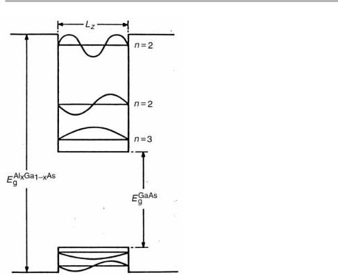
In a QW heterostructure, the electrons and holes are con®ned in a thin ®lm of the narrower band gap material, e.g. GaAs, with Eg51.42 eV at room temperature or 1.52 eV at 0 K, surrounded by an alloy of (AlGa)As, as illustrated in ®gure 8.14 (the band gap of AlAs is 2.15 eV at room temperature, see table 8.1). A key quantity is the valence band oVset, DEV, or the conduction band oVset DEC, i.e. (DEg 2 DEV). The energy levels in the well are determined by how the band gap diVerence DEg is partitioned between DEV and DEC. The quantity QC5DEC /DEg, the proportion of the gap diVerence which appears in the conduction band, is often quoted in data tables, but DFT and other theoretical models typically give DEV with best accuracy.
Although the quantization of the energy levels in the z-direction leads to the 2DEG, electrons and holes can move in the x and y directions parallel to the interface; so what is shown in diagrams such as ®gures 8.13(a) or 8.14 is not a unique level, but the onset energy of a subband. Within a subband, the 2D density of states is a step function as shown in ®gure 8.13(b). For GaAs and similar materials, there are also light and heavy holes, related to spin-orbit splitting in the valence band, and the material, in contrast to Si, has a direct band gap. Thus the optical properties of the well are now determined by the electron and hole masses (three parameters), the well width Lz, and QC. Duggan (1987) has given a useful introduction to the determination of optical properties, typically pursued via optical absorption or photoluminescence (PL) experiments; another useful starting point is Kelly (1995, chapter 10). As shown in ®gure 8.15, the optical absorption (transmission) spectrum shows peaks which can be identi®ed with light and heavy hole transitions. Note, in passing, that PL experiments only work at low temperatures, as the transitions are too broad at room temperature, and the
276 8 Surface processes in thin ®lm devices
Figure 8.14. Simple energy levels in a quantum well, consisting of a narrower band gap material (GaAs) surrounded by a higher band gap material (AlxGa12xAs). Note, however, that the well wavefunctions must in practice spread into the surrounding layers, and the real band structure modi®es this picture (from Duggan 1987, reproduced with permission).
number of parameters involved causes quite a bit of diYculty for data analysis. Nevertheless, several parameters can be determined (or assumed in order to get better values of other parameters), the early work leading to QC values typically in the range 0.6±0.8 for GaAs/AlGaAs heterostructures, and subsequently re®ned towards the lower end of this range (Yu et al. 1992, Davies 1998).
In the same volume (Capasso and Margaritondo 1987) there are extensive tabulations of early experimental valence band oVsets DEV, obtained largely by photoemission, but also by other techniques including extensions of C±V pro®ling and DLTS. Raman scattering has also found a useful niche (Menéndez et al. 1986, Menéndez & Pinczuk 1988) to measure inter-subband transitions for electrons, and hence DEC. Later compilations and comments are given by Yu et al. (1992), Butcher et al. (1994) and Franciosi & Van de Walle (1996). Technology moved ahead in the 1990s, e.g. via the infrared devices based on resonant tunneling via minibands (Capasso & Cho 1994), but the science had more or less stabilized by the late 1980s. Table 8.1 gives some representative DEV values for low strain interfaces.
However, it has become clear that pictures such as ®gures 8.10 and 8.11 are only a ®rst step, and that too simple pictures may give a misleading impression. Valence band

8.2 Semiconductor heterojunctions and devices |
277 |
|
|
Table 8.1. Some calculated valence band oVsets across low mis®t (001) interfaces in comparison with experimental DEV values
|
Unstrained mis®t |
Band gaps at |
Calculations |
Experiment |
Interface |
at 300 K (%)f |
300 K (eV)f |
DEV (eV) |
DEV (eV) |
Ge/GaAs |
10.09 |
0.66/1.42 |
0.63a, 0.32b |
0.53b |
|
|
|
0.58±0.62e* |
0.5160.09c |
GaAs/AlAs |
20.12 |
1.42/2.15 |
0.37a, 0.55b |
0.50b |
|
|
|
0.5860.06e |
0.5060.05c |
InAs/AlSb |
21.27 |
0.35/1.62 |
20.05b |
20.13f* |
|
|
|
20.1760.1c |
20.1860.05c |
InAs/GaSb |
20.62 |
0.35/0.75 |
20.38a,±0.40b |
20.51b |
|
|
|
20.5460.02d |
20.5560.05c |
|
|
|
|
|
References: (a) Van de Walle & Martin 1986; (b) TersoV 1987; (c) range of values from Yu et al. 1992, mostly excluding measurements without error bars; (d) Montanari et al. 1996; (e) Peressi et al. 1998, (e*) for the two-layer mixed interfaces discussed in the text; (f) Davies 1998, Appendix 2, (f*) section 3.3.
oVsets are often divided into three classes: type I, or straddling alignment, is as illustrated in ®gure 8.11(b) is appropriate for Ge/GaAs or GaAs/AlAs; type II, or staggered alignment, is as shown in ®gure 8.11(a), which is observed in the InAs/AlSb system. There is also a type III, or broken-gap alignment, observed for InAs/GaSb in which the bands do not overlap at all1 (Davies 1998, section 3.3). There are two types of problem, one apparent, one real; let us get appearances out of the way ®rst. Figure 8.11 shows schematically the energy positions EV and EC, but it does not show the dependence of these energies on the k-vector, i.e. the detailed band structure, which is shown simpli®ed, in a rather unrealistically symmetric alignment, in ®gure 8.10.
Band structures are rather diVerent for the various bulk semiconductors, as can be explored via the problems and projects given for chapter 7. When calculating energies such as EB, a detailed integration is done for both the valence and conductions bands over the entire 3D Brillouin zone. In the integration, the G-point (k50) contributes negligibly; high densities of states are typically concentrated at the zone boundaries and near various maxima and minima, such as the valleys associated with indirect gaps. The calculation re¯ects the `center of gravity' of the two bands. Zone boundary states correspond to standing waves, and in a bulk compound semiconductor such states may be preferentially located over one type of atom. The shift in EB is associated with (partial) electron transfer from cations to anions which diVers across the interface, also associated with diVerent band structures (curvatures) in the two materials.
1Note that the language here can be confusing: Yu et al. (1992) have two subsets of type II to cover these two materials, and a diVerent type III; there is also a sign convention which is unevenly applied. Here we
use a negative sign for DEV if the valence band edge of the narrower gap material is lower in energy than that of the wider gap material. This has the advantage of not having to remember which type is involved when interpreting DEV and QC. There does not seem to be an accepted standard convention.

278 8 Surface processes in thin ®lm devices
Figure 8.15. EVective mass analysis of a particular GaAs quantum well, surrounded by AlxGa12xAs with x50.21. The left hand panel shows the predicted heavy and light hole transitions and band oVsets, and the well thickness, all of which were deduced from the absorption spectrum shown in the right hand panel (from Duggan 1987, reproduced with permission).
So what real problems remain? Although the MIGS and related models are relatively satisfying, professionals in this ®eld clearly do not believe that they contain the whole story, and can demonstrate that interface chemistry/ segregation plays an important role in addition (Brillson 1994, Mönch 1994). They can then consider tailoring the interfacial layers to produce particular desired oVsets (Franciosi & Van de Walle 1996). For example, we can show that the composition of the interface layer does play a role. As argued by Peressi et al. (1998), the TersoV model for the diVerences in DEV between diVerent heterostructures with the same substrate, or between diVerent Schottky barrier heights DfBP with the same metal as shown in ®gure 8.12, indicates that these diVerences are largely due to bulk properties. On the other hand, the absolute values are not merely bulk quantities, and the models discussed so far only work for non-polar interfaces, or for polar interfaces between homovalent materials, such as Ge/Si(001), which is of course strongly strained. The supposedly simple Ge/GaAs (001) junction would have two extreme ways of forming a sharp interface, i.e. termination with Ga or As, but as such an interface would be charged it must either reconstruct and/or inter-
8.2 Semiconductor heterojunctions and devices |
279 |
|
|
mix. There are two possibilities for an isolated neutral mixed plane, (AsGe)1/2 or (GaGe)1/2, which were calculated to have valence band oVsets diVering by 0.6 eV; this diVerence is much greater than the uncertainty in experimental values, but the average is closely the same as for the non-polar (110) interface.
The real material has many possible ways to intermix and thereby minimize charge imbalance across the interface, and a better option was thought to be mixing over two planes, so that the interface dipole could be reduced to zero. Again there are two options involving (Ga3Ge)1/4 followed by (GaGe3)1/4, or vice versa. Now the calculations shown in table 8.1 give 0.62 and 0.58 eV, much closer to each other and to experiment (Biasiol et al. 1992). To ®nd the actual structure and the VBO at the same time is a challenge, since there are several structures worthy of attention which have similar energies. Nonetheles, Peressi et al. (1998) conclude that MIGS-related (or better termed, linear response theory) models form a very good starting point, provided one discusses the interface that is actually present. For the `model solid' approach (Van de Walle 1989), the eVects of strain can be incorporated in a natural way without further approximation; this method is therefore favored for calculations on strained layer interfaces.
The examples where these models clearly don't work correlate with strong chemical/metallurgical reactions and/or steps or other defects at the interface, with associated trapped charges and/or dipoles. One could counter by saying that in these cases, the interface is simply not what was initially postulated. If one adds the evidence now being obtained from BEEM about large lateral variations in barrier heights, and in transmission coeYcients across such interfaces, then variability is not surprising. Technology in one sense is all about processing: in that context variability which one cannot control is the real disaster. But in making the transition to scienti®cally based industry, understanding is also very important. Without it, any small change in processing conditions forces a return to trial and error, with typically a huge parameter space to explore ± preferably by yesterday, or you are out of business!
8.2.4Modulation and d-doping, strained layers, quantum wires and dots
In heterostructures, we also have to have provide carriers via doping. But if the layers are narrow enough, we may be able to put the dopants at diVerent positions and thereby increase carrier mobilities by strongly reducing charged impurity scattering. This is one of the key points behind modulation doping, and is a factor in d-doping, i.e. doping on a sub-ML scale, which can be used to change the shape of quantum wells (Schubert 1994). A limit to such techniques is the fact that dipoles are set up between the layers, which will also bend the bands. Depending on the doping level, the various length scales may or may not be comparable, and the models used will be diVerent in detail. Understanding the eVect of diVerent length scales in models of condensed matter has a long history (Anderson 1972, Kelly 1995 chapter 3) and the topic continues to attract comment (Jensen 1998). Transitions in dimensionality, from 3D to 2D and so on down to 0D, are also of interest in the same sense. For example, a layered

2808 Surface processes in thin ®lm devices
heterostructure which behaves as a 2DEG in zero magnetic ®eld, becomes a 0DEG dotlike structure in a strong magnetic ®eld, as the size of the cyclotron orbit becomes less than the lateral device dimensions. This is a key aspect of various devices based on `quantum conduction': often the leading edge devices only work at low temperatures and/or in a high B ®eld. Such devices are competitive in applications where ultimate sensitivity is required (e.g. telephone/TV satellite transmission and reception, or in astronomy), but not in domestic receivers whose emphasis is on optimum room temperature performance, where high electron mobility transistors (HEMTs) based on GaAs/(AlGa)As are a success story (Kelly 1995 chapter 5).
Some of these dimensional transitions are exempli®ed in strained layers, of which the archetype consists of GeSi alloys of various compositions on Si(100). The compressive strain due to 4.2% larger lattice constant of Ge means that the layers have a tetragonal distortion, which lifts the degeneracy of the four valence band minima with k parallel to the layer from the two with k perpendicular to the layer. This, and the switch of the position of the conduction band minimum at high Ge composition, in¯u- ences both the band gap and oVsets as a function of both composition and strain (see e.g. Kelly 1995 chapter 14, or Davies 1998 chapter 3). A realistic feel for the amount of work done on this one system may be obtained from the reprint collection made by Stoneham & Jain (1995), and the other references cited in section 7.3.3.
Quantum wires can be formed on a linear surface structures, the most obvious of which are vicinal surfaces consisting of arrays of steps. Experiments on a variety of con®gurations based on GaAs and AlGaAs are described by PetroV (1994). The problem is that individual steps are typically too rough to make this approach work, unless regular multi-atomic height steps can be reliably fabricated; this is a current research eVort. It is not yet clear that such approaches can supplant lithography techniques (Prokes & Wang 1999). Similarly, quantum dots, in Ge/Si for example, need to be rather uniform in size to be useful; the question of whether one can persaude them to do this during growth of their own accord (i.e. via self-organization), or whether one uses lithographically patterned substrates is also a hot topic, which is discussed further in section 8.4. A discussion of early results using patterned layers is given by Kapon (1994); these eVorts overlap with the topics discussed here in sections 5.3 and 7.3.
8.3Conduction processes in thin ®lm devices
The conductivity and the resistivity r are among the simplest material parameters to measure, one only needs a voltmeter and an ammeter. They are also some of the most useful properties, especially when they are non-linear and can thereby be used to amplify or store currents or voltages, as in essentially all active electronic devices. Yet it is an irony that what is easiest to measure and experience can also be the hardest to set on a ®rm scienti®c foundation, or to describe quantitatively with few unknown parameters. Here we explore in the simplest terms why this is the case, and indicate the role that surface and interface processes play in electrical and magnetic properties of thin ®lms.