


3.1 Classi®cation of surface and microscopy techniques |
69 |
|
|
(d)
Figure 3.2. (cont.) (c) a widely used AFM design, with a He±Ne laser to detect the de¯ection of the cantilever on which the tip is mounted (after Meyer & Amer 1988); (d) close up SEM view of a Si3N4 AFM tip with a nominal tip radius ,30 nm, which has achieved atomic resolution (after Albrecht et al. 1990; diagrams reproduced or redrawn with permission).
3.1.4Acronyms
Acronyms are de®ned at various places throughout this book and are summarized in Appendix B. So far we have met and de®ned in the text: vacuum and electronics terms UHV, RGA, QMS, TSP, SNR; surface and crystal growth terms ML, TLK, BCF, CVD, MBE and others in section 2.5; diVraction techniques LEED, RHEED, THEED; chemical analysis and ion scattering techniques AES, SIMS, ICISS; microscopy types

703 Electron-based techniques
TEM, REM, LEEM, PEEM, SEM, STEM, STM, AFM, SNOM. We also have two techniques (EELS, CBED) indicated on ®gure 3.1, which have not yet been de®ned. Now is a good time to check you know what these acronyms stand for, since we will be adding more to the list as we start to study individual techniques in more detail. In the following sections, we emphasize a common case, where electrons are both the probe and the detected (response) particle.
3.2Diffraction and quasi-elastic scattering techniques
3.2.1LEED
The common electron-based diVraction techniques are LEED and RHEED. As with all surface diVraction techniques, the analysis is based in terms of the surface reciprocal lattice. An important aspect of diVraction from 2D structures is that the compo-
nent of the wave vector k, parallel to the surface k// is conserved to within a surface reciprocal lattice vector G//, whereas the perpendicular component k' is not. This leads to the idea of reciprocal lattice rods; they express the fact that k' can have any value, so that diVraction can take place at any angle of incidence. However, the intensity of
diVraction is typically not constant at all values of k', but is modulated in ways which re¯ect the partial 3D character of the diVraction (Lüth 1993/5 section 4.2, WoodruV
&Delchar 1986 section 2.3).
The equipment for both diVraction techniques is simple, involving a ¯uorescent
screen, with energy ®ltering in addition in the case of LEED, as indicated in ®gure 3.3, to remove inelastically scattered electrons. There are three types of LEED apparatus in regular use. The normal-view arrangement has the LEED gun and screen mounted on a UHV ¯ange, typically 8 inches (200mm) across, and the pattern is viewed past the sample, which therefore has to be reasonably small, or it will obscure the view. Most new systems are of the reverse-view type, where the gun has been miniaturized, and the pattern is viewed through a transmission screen and a viewport. This enables larger sample holders to be used, which helps for such operations as heating, cooling, straining, etc. The third, and potentially most powerful, technique is where, in addition to viewing the screen, the LEED beams can be scanned over a ®ne detector using electrostatic de¯ectors and focusing, in order to examine the spot pro®les, which can be sensitive to surface steps and other forms of disorder at surfaces. This technique, which has been perfected by the Hannover group (Henzler 1977, 1997, Scheithauer et al. 1986, Wollschläger 1995), is now known as SPA-LEED, emphasizing the capability for spot pro®le analysis.
There are two aspects to electron diVraction techniques. The ®rst, and simplest, is that the positions of the spots give the symmetry and size of the unit mesh, i.e. the surface unit cell. The common use of electron diVraction is primarily, often solely, in this sense. The second eVect is that the positions of atoms in the mesh is not determined by this qualitative pattern (see discussion in section 1.4), but requires a quantitative analysis of LEED intensities. Application of dynamic theory has so far `solved' several

3.2 Diffraction and quasi-elastic scattering techniques |
71 |
|
Reverse view |
|
|
E/e |
E/e |
|
electron gun |
amplifier |
|
|
|
|
+5 kV |
|
|
±E/e |
|
|
|
±E/e |
|
specimen |
Spot profile |
|
Normal view |
analysis |
|
|
|
|
Figure 3.3. LEED apparatus types, illustrating schematically the con®gurations of normal and reverse view LEED, and spot pro®le analysis. The 15 kV is applied to a ¯uorescent screen, which for reverse view must be transparent (after Bauer 1975, redrawn with permission).
hundred surface structures (Watson et al. 1996). This is impressive, but it pales besides the number of bulk structures solved by X-rays, using (developments of) kinematic theory.
Experimentally, the intensities are typically collected in the form of so-called I±V or I(E) curves, where the size of the Ewald sphere is varied by varying the probe energy (say from 20±150 eV), and the intensity data are obtained by `tracking' along an individual reciprocal lattice rod. Various computer controlled, and frame grabbing, schemes have been developed to do this. A description of standard experimental and theoretical methods is given by Clarke (1985); useful updates are reviews by Heinz (1994, 1995). Lüth (1993/5, chapter 4) or Prutton (1994, chapter 3) are other starting points for LEED, as they introduce the basic idea of multiple scattering in a relatively short space.
The diVerence between LEED and X-ray structure analysis is that a kinematic diVraction theory has limited usefulness, because the scattering is very strong, as explored in problem 3.2. Averaging diVerent I±V curves at constant momentum transfer was once a promising method in the attempt to get around this problem, and some successes were recorded, particularly in obtaining the distances between lattice planes parallel to the surface, and surface vibration amplitudes (Webb & Lagally 1973, Lagally 1975). However, dynamical theory is constantly being developed, e.g. via adoption of the latest computational and approximation methods, which are closely related to band theory and have similar constraints (Pendry 1994, 1997); LEED is still the main method of surface structure analysis, now complemented by surface X-ray diVraction using synchrotron radiation (Feidenhans'l 1989, Johnson 1991, Robinson & Tweet 1992, Renaud 1998).

72 |
3 Electron-based techniques |
|
|
|
(a) |
Reciprocal space |
|
|
C |
k9 |
g |
|
k |
O |
|
|
|
||
|
(b) |
Real space |
|
|
Electron gun |
|
|
|
|
Sample |
Screen |
Figure 3.4. RHEED geometry in (a) reciprocal space and (b) real space.
3.2.2RHEED and THEED
The basis of RHEED is very similar in LEED, but the language used is rather diVerent, being similar to that used for THEED. The discussion can again be separated into geometry and intensities. The glancing angle geometry of RHEED means that the reciprocal lattice rods are closely parallel to the Ewald sphere near the origin, as shown in ®gure 3.4. This means that the low angle region often consists of streaks, rather than spots. This part of the pattern corresponds to the zero order Laue zone (ZOLZ) in THEED patterns. The higher angle parts of a RHEED pattern are then equivalent to higher order (HOLZ) rings in THEED patterns.
The apparatus for RHEED can consist of a simple 5±20 kV electrostatically focused gun, for instance to monitor the surface crystallography in an MBE experiment, where the glancing angle geometry has many practical advantages over LEED, especially in the ease of access around the sample. Or it can utilize an electron gun approaching electron microscope quality, operating at higher voltages, and produce ®nely focused diVraction spots over a wide angular range.
Several workers have perfected this technique especially in Japan (Ino 1977, 1988, Sakamoto 1988, Ichikawa & Doi 1988), and two examples of Si(111) 737 in diVerent azimuths are seen in ®gure 3.5. Ino's group in particular have also developed a curved screen, centered on the sample, which could be viewed in two directions at right angles.
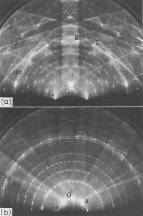
In the normal view, from the right of ®gure 3.4, we see spots distributed on a series of arcs as shown for the Si(111)Î33Î3R30° Ag structure in ®gure 3.6(a); the same screen,
viewed via a mirror in the perpendicular direction along the reciprocal lattice rods is
seen to be an undistorted view of the reciprocal lattice (as in LEED) in ®gure 3.6(b). We can note that the (111)737 and (111)Î3 patterns are strikingly diVerent in a qual-
itative sense.
As in LEED, the question of intensities is much more detailed, involving multiple scattering and inelastic processes, and there are many discussions/assertions in the literature about whether streaks or spots constitute evidence for good (i.e. well prepared, ¯at) surfaces. Some general remarks are made in the next section.
3.2 Diffraction and quasi-elastic scattering techniques |
73 |
|
|
3 Å Å Figure 3.5. RHEED patterns (20 kV) of Si(111) with the 7 7 reconstruction along: (a) [121]
Å 9
and (b) [011] incidence. Note the reciprocal lattice unit cell O ACB, and the six superlattice spots in each direction between these fundamental spots (from Ino 1977, reproduced with permission).
74 3 Electron-based techniques
Figure 3.6. RHEED patterns (20 kV) of Si(111) in the `Î3' structure associated with the ML phase of Ag deposited at 500°C: (a) in the normal view, (b) in the perpendicular view, showing reciprocal lattice unit cell O9ACB, and the two spots between these spots (from Gotoh & Ino 1978, reproduced with permission).
3.2.3Elastic, quasi-elastic and inelastic scattering
Models of LEED and RHEED concentrate on elastic scattering, where the energy of the outgoing electron is the same as that of the incoming electron. But experimentally
we cannot discriminate in energy very well in a typical diVraction apparatus. LEED grids/screens are able to remove plasma loss electrons (,10±20 eV loss), but the intensities measured include phonon scattering (,25 meV losses and gains). This is thermal diVuse scattering, and is accounted for in the models using a Debye±Waller factor, as in standard X-ray treatments. At higher temperature, the intensities in the Bragg peaks fall oV exponentially, as
I/I |
5exp 2 (K2Ku2L /2), with Ku2 L 53"2T/(mku 2), |
(3.1) |
0 |
d |
|
3.2 Diffraction and quasi-elastic scattering techniques |
75 |
|
|
ud being the Debye temperature, and K the scattering vector. This means that intensity measurements as a function of temperature measure Ku2L, and several such studies have been done with LEED. An interesting feature of such experiments is that the value of Ku2L decreases towards the bulk value as the incident energy is increased, re¯ecting the increased sampling depth of the electrons (Lagally 1975, WoodruV & Delchar 1986,1994 chapter 2.7).
In a typical RHEED setup there is no energy ®ltering, other than that caused by the fact that higher energy electrons produce more light from phosphor screens. Yet the geometry is such that plasmons, especially surface plasmons, will be produced very eYciently. Because plasmon excitation produces only a small angular de¯ection, the diVraction pattern is not unduly degraded. A few groups have studied energy-®ltered RHEED (Marten & Meyer-Ehmsen 1988, Ichimiya et al. 1997, Weierstall et al. 1999), but it is diYcult to construct ®lters which work over a large angular range.
LEED (especially SPA-LEED) and RHEED, and the corresponding microscopies (LEEM and REM) have been shown to be very sensitive to the presence of surface steps and other types of defects, including domain structures. Some of these eVects are due to the extra diVraction spots associated with particular domains; some are due to exploiting the diVerence between in-phase and out-of-phase scattering between terraces separated by steps; some again depend on the small static distortions and rotations produced by surface steps, and the increase in diVuse scattering (Yagi 1988, 1989, 1993, Henzler 1977, 1997, Bauer 1994, Wollschläger 1995). SPA-RHEED has also been demonstrated (Müller & Henzler 1995).
The basic reason for the surface sensitivity of LEED is the short inelastic mean free path for the excitation of plasmons (and other forms of electron±electron collision); this means that information from deeper in the crystal is eVectively ®ltered out. One of the few calculations which is straightforward (see problem 3.2) is the pseudo-kinematic case, where one has single scattering and exponential attenuation. This calculation shows that the attenuation causes only a few layers at the surface to be sampled, which give rise to modulated reciprocal lattice rods, the width of the modulations being inversely proportional to the imfp.
In the full dynamical LEED calculations, the attenuation eVect is included by an imaginary potential, V0i. This is similar to the high energy case of RHEED and THEED, but the language is a little diVerent. In TEM, imaginary potentials (V0i and Vgi) are used to describe contrast in images caused by inelastic scattering; but these are dependent on the aperture size used, and are typically due to the scattering of phonons and defects. In contrast to plasmons, these scattering events cause a wide angular spread, and very little energy loss. Calculating RHEED intensities is a suitable combination of layer slicing, as in LEED, and high energy forward scattering as in THEED; reviews of these methods have been given by Peng et al. (1996) and Maksym (1977, 1999).
There are new electron diVraction techniques emerging, such as DLEED (DiVuseLEED) (Heinz 1995) and electron holography (Saldin 1997), and continuous development of related theoretical methods (Pendry 1997). The above (outline) discussion has concentrated on the eVect of inelastic processes on the interpretation of elastic